
Diffusion kinetics and evolution of self-assembled nickel germanide nanorings on germanised Si (100)
D. Panda*ab,
A. Dharb and
S. K. Rayb
aDepartment of Electronics Engineering, National Institute of Science and Technology, Brahmapur, Odisha-761 008, India. E-mail: dpanda@nist.edu; d.panda@utah.edu
bDepartment of Physics and Meteorology, Indian Institute of Technology Kharagpur, Kharagpur-721 302, India
First published on 27th March 2015
Abstract
Self assembled binary nickel germanide nanorings are formed by annealing of a Ni/Ge/Si (100) film. Nickel germanide phase formation is confirmed by an X-ray diffraction (XRD) and X-ray photo electron spectroscopy (XPS) study. Rutherford backscattering spectrometry (RBS) measurement has been used to analyse germanide compositions and film thickness of the different annealed samples. Composition of the binary germanide phases from RBS simulation, agrees well with the XRD data. Atomic force microscopy (AFM) topography has been used to study nanoring evolution. Scanning electron microscopy (SEM) structures agree well with the AFM results. Nanoring formation mechanisms have also been explained with schematic structures. Nanostructures and lattice spacing of germanides have been studied from transmission electron microscopy (TEM) micrographs and selected area diffraction pattern (SAED) pattern.
Introduction
In the last few decades, people have devoted much of their effort to the fabrication of nanostructures such as nanowires, nanorods, quantum wires, etc. for different nano and quantum device applications viz. quantum dots (QDs) laser, and single-electron transistor.1–3 Very recently, nanorings2,3 have attracted a renewed interest for applications as data storage in memory and quantum devices. When using magnetic random-access memory (MRAM) loss of data can be easily reduced in case of a power outage, and as a result the system becomes faster and consumes less energy. But such memories are still expensive and not totally reliable.In 2006, Zhu et al.2 designed irregular shaped metal nanorings that can serve as memory cells, which could lead to coin-sized hard drives that store a huge amount of data. The intriguing geometry of such nanorings has no central area and therefore, contain no vortex core in the ‘vortex state’, meaning that they have no stray field at all.4–13 As a result, the vortex state can be steadily retained in nanorings of even very small radius. Ideal nanorings must not only have well-defined inner and outer radii but also have a narrow width, which is less than that of a domain wall to ensure that no vortex core can exist within the ring width. These challenging requirements are hard to meet even though advanced electron-beam lithography and molecular beam epitaxy (MBE) are most commonly used for fabricating nanorings.2–9 Asymmetrical design allows more of the nanorings to end up in a so-called ‘vortex state’.
Not only metal nanorings have been established, recently a type of nanostructure of semiconductor quantum rings (QRs) has also been studied.14–18 Experimental results of such self-assembled QRs were first reported in 1997 (ref. 14) in an InAs–GaAs system. More recently, a QR structure was also obtained by capping a thin InP layer onto InAs QDs on InP substrate.18 Lee et al.17 fabricated self-assembled Ge nanorings from Si-capped Ge quantum dots on Si substrate. Ni nanorings have been reported by Zhu et al.2 On the contrary, it has been reported that, metal silicides provide a better alternative over pure metal interconnect.19–27 Metal germanide26–28 gives much more prospective than metal silicide, although both have almost similar properties, for its potential application in high speed devices. While nickel silicide nanostructures have been reported,19–22 germanide nanostructures still remain unreported.
Prior to the growth mechanism of the ring structures, two kinds of growth models have been developed.18,29–32 One is based on minimum surface free energy,18,29,30 called a thermodynamic model. It maintains that the changes in surface free energy are balanced due to thin layer overgrowth, which creates an outward pointing force. This force brings about a material redistribution resulting in a ring shaped structure. Another is based on kinetic considerations, namely on the differences in surface diffusion rate of mobile atoms.14,31,32 According to this model, mobile atoms diffuse from the dot outwards, leaving a void at the original dot location. Mobile atoms diffuse into the surrounding area and form an immobile ring-shaped mixed (mobile atoms and surrounding materials) island. In both the models, strain energy due to lattice mismatch is not taken into account and the rings are formed during deposition and over-growth.
Although there are a few reports on the fabrication of nanorings of InGaAs,14 Ge17 and some metals;2 most of them are fabricated by highly sophisticated and cost-effective systems like molecular beam epitaxy (MBE), ultra high vacuum chemical vapour deposition (UHV-CVD) or electron-beam lithography. In this article, for the first time the growth of NiGe asymmetric nanorings by simple thermal evaporation of Ni on sputtered Ge/Si (001) film followed by annealing is reported. Effect of post-deposition annealing on the phase as well as nanoring and quantum dot formation have been studied and analysed using grazing incidence X-ray diffraction (XRD), X-ray photo electron spectroscopy (XPS), Rutherford backscattering spectrometry (RBS), atomic force microscope (AFM), scanning electron microscopy (SEM) and high resolution transmission electron microscopy (HRTEM).
Experimental
Boron doped p-type Si (001) wafers with resistivity 7–14 Ω cm−1 were used in the present study. Silicon wafers were degreased by ultrasonic agitation in acetone followed by rinsing in DI water. They were treated in a mixture of H2SO4 and H2O2 (1![[thin space (1/6-em)]](https://www.rsc.org/images/entities/char_2009.gif) :1) for 25 minutes followed by rinsing thoroughly in DI water. Finally, the samples were dipped in 1% HF solution and immediately loaded into the deposition chamber for germanium deposition. Prior to growth of the nickel layer, a ∼500 nm thick homogeneous Ge layer was deposited by RF magnetron sputtering (Edwards, UK) at argon pressure and RF power 0.05 mbar and 60 Watt, respectively. Immediately after that a very thin nickel film (∼10 nm) was deposited by thermal evaporation using high purity (99.9999%) nickel foil. Post deposition annealing treatment was carried out in the temperature range 600 °C to 900 °C in nitrogen atmosphere for an hour to form the nickel germanide nanoring.
:1) for 25 minutes followed by rinsing thoroughly in DI water. Finally, the samples were dipped in 1% HF solution and immediately loaded into the deposition chamber for germanium deposition. Prior to growth of the nickel layer, a ∼500 nm thick homogeneous Ge layer was deposited by RF magnetron sputtering (Edwards, UK) at argon pressure and RF power 0.05 mbar and 60 Watt, respectively. Immediately after that a very thin nickel film (∼10 nm) was deposited by thermal evaporation using high purity (99.9999%) nickel foil. Post deposition annealing treatment was carried out in the temperature range 600 °C to 900 °C in nitrogen atmosphere for an hour to form the nickel germanide nanoring.
Ex situ grazing incidence XRD (Philips X’Pert-Pro MRD), XPS (VG Scienta-make), and RBS were carried out on different samples to study the phase formation, film thickness and composition of the metal germanide nano-structures. Grazing angle (1.0°) XRD data were collected with a step size of 0.01° in the point focus mode of the X-ray beam using Cu-Kα radiation. Compositions of the rings were studied using XPS. XPS data were obtained using MgKα (hν = 1253.6 eV) excitation source in an ESCA-2000 Multilab apparatus (VG Microtech) with a residual gas pressure in the range of 10–10 Torr. All these spectra were recorded at room temperature using a hemispherical analyzer at 30° take-off angle, with pass energy of 50 eV and instrumental resolution of 0.6 eV. The binding energy has been corrected for sample charging effect with C 1s reference line at 284.5 eV for the surface oxidation.
RBS measurement using 2 MeV and 3 MeV He2+ ion beam delivered from a tandem pelletron accelerator was carried out with a silicon surface barrier detector fixed at a backscattering angle of 165° and the spectrum were analyzed using standard computer simulation software SIMNRA 6.03.33–35 RBS experimental parameters were kept identical during each set of experiment. Tapping mode AFM (Nanoscope IV, Veeco) and SEM (LIO430i) were performed to study the nanoring formation of the samples. High resolution transmission electron microscopy (HRTEM) (JEOL JEM-2100) was performed using an instrument operating at 200 kV and equipped with a Gatan digital micrograph apparatus.
Results and discussions
Fig. 1 shows the grazing incidence XRD spectra of the binary nickel germanide films annealed at different temperatures. Using Bragg’s conditions, lattice planes corresponding to each peak appearing from binary nickel germanide films were determined and compared with the standard data available in JCPDS files. After annealing, the major change in phase formation is the transformation from Ni rich phase, to Ge rich phase. At 700 °C, Ni3Ge and Ge2Ni5 peaks dominates NiGe phase. Whereas, when the films annealed are at 800 °C, NiGe phases are prominent with respect to Ni rich binary germanide phases. 800 °C annealed spectra also indicate the formation of Ge rich phases. Formation of Ge rich phases at high temperature should be possible due to the reaction between the Ni reach germanide and sputtered Ge on Si. Fig. 2, shows XPS spectra of a typical NiGe nano-ring formed after 800 °C annealing. Chemical shift of Ge 3d by 2.5 eV with respect to the binding energy of bulk Ge is observed. Higher binding energy of Ge 3d peak than the bulk Ge indicates the incorporation of Ge into Si. Shift of Ni 2p towards higher binding energy is attributed to change in the relaxation process correlated with the increased distance between Ni–Ni nearest neighbors. | ||
| Fig. 1 Typical XRD spectra of 700 °C and 800 °C annealed NiGe nanorings. | ||
 | ||
| Fig. 2 Typical XPS spectra of the 800 °C annealed NiGe nano-ring (a) Ge and (b) Ni. | ||
RBS random spectra of the different annealed germanide samples are shown in Fig. 3 along with the SIMNRA 6.03 simulated spectrum. The spectrum of the 600 °C annealed sample shows a sharp peak structure with respect to higher annealed samples due to less diffusion of Ni on Ge. Peaks correspond to individual Ni and Ge elements are not completely resolved from 2 MeV spectra, because of their very close atomic masses. But the formation of germanides due to the diffusion of metals in germanium is clearly detected. In the 700 °C, 800 °C and 900 °C annealed samples of Fig. 3, the presence of Ni and Ge is clearly detected. To resolve the Ni and Ge we have taken data using a 3 MeV He2+ ion beam. A typical 3 MeV spectra of the 800 °C annealed germanide nanoring is shown in the inset of Fig. 3. From the figure the presence of Ni and Ge is clearly detected. Base broadening of the peak, as shown in this figure, is due to the diffusion of Ni on Ge during the formation of germanide layers. The valley on the silicon edge, as shown in Fig. 3b–d, is due to the diffusion of germanium in Si. In the RBS spectra we could not find any signature of oxygen and nitrogen contaminations following the annealing steps, and it is attributed to the formation of self-passivating germanide layers.
 | ||
| Fig. 3 2 MeV RBS spectra of different annealed NiGe nanorings. Inset shows the typical 3 MeV RBS spectra of 800 °C annealed NiGe nanorings. | ||
A visible plateau in Si edge is observed at higher temperature annealed samples, but no such plateau is noticed at a lower (600 °C) annealing temperature. This plateau affects the RBS slopes and it is attributed to the film roughness.34 Since our scattering angle is 165° and non-grazing incidence, so here we neglect the correlation effects, such as incidence through a hump and emergence through a valley or multiple surface scattering. Those effects are strongly affected at 180° back scattering angles. Roughnesses of the films is affected at low energy edges and gets broader, but the higher energy edge of the films is not affected. As seen from the Fig. 3b–d, Si edges are broaden during increase of annealing temperature, which is also attributed to increase of the film roughness with the increase of annealing temperature33 due to the transformation of dome shaped germanide to nickel germanide nanoring. Experimental data has been simulated using a structure consisting of binary nickel germanide layers of different thicknesses and compositions, summarized in Table 1. From the table, we see that the percentage of the un-reacted Ge decreases and mixed binary germanide region increases with the increase of annealing temperature.
| Ni (top-bottom) | Ge (top-bottom) | Thickness (1015 atoms per cm2) | |
|---|---|---|---|
| 600 °C annealed | 0.65 | 0.35 | 65 |
| 0.35 | 0.65 | 10 | |
| 00 | 1.0 | 171 | |
| 700 °C annealed | 0.53 | 0.47 | 10 |
| 0.45 | 0.55 | 25 | |
| 0.40 | 0.60 | 20 | |
| 0.22 | 0.78 | 18 | |
| 00 | 1.0 | 60 | |
| 800 °C annealed | 0.50 | 0.50 | 16 |
| 0.40 | 0.60 | 25 | |
| 0.32 | 0.68 | 30 | |
| 0.2 | 0.8 | 40 | |
| 00 | 1.0 | 30 | |
| 900 °C annealed | 0.50 | 0.50 | 16 |
| 0.40 | 0.60 | 30 | |
| 0.32 | 0.68 | 35 | |
| 0.20 | 0.80 | 55 | |
| 00 | 1.0 | 17 |
Fig. 4 shows typical AFM images of different nickel germanide nanoislands and nanorings. The AFM images of the samples annealed at 600 °C (Fig. 4a) shows an uniform homogeneous surface. But, when the samples are annealed at 700 °C islands were formed, shown in Fig. 4b. About 300–350 nm diameter islands are formed between homogeneously distributed 25 to 35 nm particles, with an average height of 150–170 nm. SEM micrograph of this sample, shown in Fig. 5a, also agrees well with the AFM topography. However, the growth and formation of self-organized nickel germanide nanoislands is mainly governed by the strain energy relief mechanism, and the growth transition from two-dimensional to three-dimensional is the initial relief of strain energy, known as island growth. We believe that, this dome/island formation, as well as shape transformation process is also due to the strain energy relief mechanism. In general, the diffusion rate of Ni is very high36 in silicon or germanium. So, the ultra-thin Ni layer covering the Ge layers as a continuous blanket will have larger strain energy due to big lattice mismatching. At relatively high temperature (i.e. in this case at 700 °C) many atomic processes such as, surface diffusion of Ni into Ge and surface segregation of Ni are stimulated, to bring a large amount of mass transportation and minimization of total strain energy, resulting in the dome shape formation.
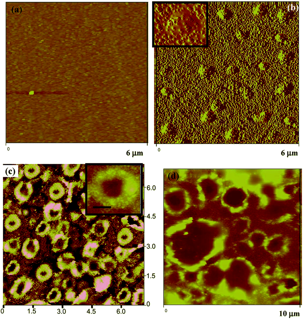 | ||
| Fig. 4 AFM topographies of the (a) as deposited, (b) 700 °C annealed, (c) 800 °C annealed and (d) 900 °C annealed NiGe film. Inset of figure shows a single (b) dome and (c) nanoring (scale in inset is 400 nm). | ||
 | ||
| Fig. 5 SEM images of the (a) 700 °C annealed, (b) 800 °C annealed and (c) 900 °C annealed NiGe film. | ||
Fig. 5a is the top view of SEM micrograph of the different nanoislands formed after annealing at 700 °C, which looks like a droplet. On the contrary, Ge rich domes are formed by agglomerating the Ni rich smaller germanide nanoparticles of diameter 25 nm to 35 nm, which confirms from our XRD structures shown in Fig. 1, with Ge and results in the formation of islands. Fig. 4c and d and Fig. 5b and c show the surface topography and SEM top view after annealing the sample at 800 °C and 900 °C, respectively. At this stage, the nanoislands are converted to nanorings and the ring diameters are larger than the islands. These nanorings have an inner diameter and height of 350–400 nm and 150–160 nm, respectively at 800 °C, whereas at 900 °C, it is 560–710 nm with almost the same height. In the picture, we noticed a few islands at 800 °C annealed samples that completely transformed to rings at 900 °C. The incomplete evaporation of islands at 800 °C is due to the presence of some impurities. Few rings are bigger and asymmetric in 900 °C, inner diameter ∼ 1 μm, due to the combining of small rings. There are no established models present to explain the ring formation. The ring formation by depositing mobile material on quantum or nano dot during growth has been explained previously.15,17,29 But till now there are no reports regarding the formation and explanation of nanoring after annealing. Fig. 6 shows the size distribution plot of the nanoislands and nanorings. It is clear that after annealing at 800 °C, the nanorings have uniform size distribution, rather than the nano-islands.
 | ||
| Fig. 6 Size distribution plot of NiGe nano-islands at 700 °C, nanorings at 800 °C and nanorings at 900 °C. | ||
A possible scenario of ring formation after annealing, shown schematically in Fig. 7, can also be discussed by the strain energy relief viewpoint. Ni rich NiGe nanoparticles present on the top of germanide islands (shown in the inset of Fig. 4b), at 700 °C, are partially strained and the strain in islands are partially relaxed by the deformation of the Si substrate with Ge–NiGe system and at the top of the islands highest degree of strain relaxation happens. Lattice constant and Ni concentration of the islands along the surface gradually decreases from top to bottom. At top of the islands, the lattice constant of Ni rich germanide is close to that of Ge rich germanide at base. Ni rich germanide adatoms on the top of the islands will feel higher surface chemical potential, which rises from variation of lattice mismatch with respect to the underlying Ge rich germanide islands. This gradient of lattice mismatch and/or surface chemical potential will drive the mobile Ni adatoms of Ni rich germanide on top of the islands to diffuse into its Ge rich base surface. Hence, more germanide atoms will be accumulating at the side surface with Ni atoms migrating into the islands by surface diffusion, resulting in a decrease in the top base and increase in the base diameter of islands as shown in AFM and SEM images, Fig. 4c and 5b.
 | ||
| Fig. 7 Schematic growth mechanism of NiGe (a) dome at 700 °C, (b) nanorings at 800 °C annealed and (c) nano-rings at 900 °C. | ||
This process in which nickel atoms diffuse into the base of germanide alloy can also be thought to be driven by strain energy relief, because the lattice at base matches with germanide alloy with varied Ge composition (increases towards base). At high temperature, the diffusion rate of Ni increases; Ni atoms in the top region of previous islands will diffuse away to the side surface. Meanwhile, Ni atoms on the islands will segregate on the surface to increase surface diffusion of Ni to side surface. More mass transportation from the center part to side islands surface will take place, resulting in the shape transformation from nanoislands to nanorings, as shown schematically in Fig. 7 and images in Fig. 4 and 5. Such a large amount of mass transportation is also favorable to release the strain energy. On the contrary, it could reduce the strain energy of accumulation of atoms on the side surface of islands and it will reduce the strain energy in the center part of island, which is previously partially strained. Alternatively, at high temperature the mobile Ni atoms of Ni rich germanide nano particles present on the domes, diffuses into Ge, resulting in ring formation, shown schematically in Fig. 7a and b. Fig. 7c shows the complete nanoring formation at higher annealing temperature.
Typical TEM micrograph of 800 °C annealed samples is shown in Fig. 8a. From this figure we can see a small ring of diameter 180 nm and few agglomerated clusters. In the SEM images we also noticed the formation of a few small rings, but their height is very small. The EDX on the dot shows the presence of nickel and germanium, which is attributed to the formation of nickel germanide and agrees with our XRD and RBS analysis. Selected area diffraction (SAED) pattern of nickel germanide cluster is shown in Fig. 7b. This result corroborates with the XPS and RBS data.
 | ||
| Fig. 8 Typical (a) TEM micrograph and (b) SAED pattern of 800 °C annealed NiGe nanoring. | ||
Conclusions
We have synthesized binary nickel germanide nano rings by thermal evaporation of nickel on germanised Si (100). The grazing angle XRD spectra shows the formation of nickel germanide phases. XPS study also confirms the formation of nickel germanide structure. Film thickness and compositions of germanide films at different depths were extracted from the RBS simulation of different annealed samples. Simulated composition of binary germanide phases agrees well with the XRD data. The nanoring formation has been studied using AFM topography, SEM and TEM. Possible mechanisms of nanoring formation have also been proposed. TEM structures and SAED shows the formation of nano dot, lattice spacing and structures of germanides, which attributes to the formation of nanorings. This self assembled NiGe nanoring has potential for future nanoscale device applications.Acknowledgements
We would like to thank Dr K. Das, S. N. Bose National Centre for Basic Sciences, Kolkata, for fruitful discussion. Authors are also thankful to Institute of Physics (IOP), Bhubaneswar India for providing RBS facility in this work.References
- D. Panda and T. Y. Tseng, Thin Solid Films, 2013, 531, 1 CrossRef CAS.
- F. Q. Zhu, G. W. Chern, O. Tchernyshyov, X. C. Zhu, J. G. Zhu and C. L. Chien, Phys. Rev. Lett., 2006, 96, 027205 CrossRef CAS PubMed.
- X. F. Han, Z. C. Wen and H. X. Wei, J. Appl. Phys., 2008, 103, 07E933 Search PubMed.
- J. Rothman, M. Kläui, L. Lopez-Diaz, C. A. F. Vaz, A. Bleloch, J. A. C. Bland, Z. Cui and R. Speaks, Phys. Rev. Lett., 2001, 86, 1098 CrossRef CAS PubMed.
- F. J. Castaño, C. A. Ross and A. Eilez, J. Phys. D: Appl. Phys., 2003, 36, 2031 CrossRef.
- M. Kläui, J. Rothman, L. Lopez-Diaz, C. A. F. Vaz, J. A. C. Bland and Z. Cui, Appl. Phys. Lett., 2001, 78(21), 3268 CrossRef.
- M. Kläui, C. A. F. Vaz, J. A. C. Bland, W. Wernsdorfer, G. Faini and E. Cambril, Appl. Phys. Lett., 2002, 81(1), 108 CrossRef.
- X. Zhu, P. Grütter, V. Metlushko, Y. Hao, F. J. Castaño, C. A. Ross, B. Ilic and H. I. Smith, J. Appl. Phys., 2003, 93(10), 8540 CrossRef CAS.
- S. P. Li, D. Peyrade, M. Natali, A. Lebib, Y. Chen, U. Ebels, L. D. Buda and K. Ounadjela, Phys. Rev. Lett., 2001, 86, 1102 CrossRef CAS PubMed.
- K. L. Hobbs, P. R. Larson, G. D. Lian, J. C. Keay, and M. B. Johnson, Nano Lett., 2004, 4(1), 167 Search PubMed.
- W. L. Zhou, J. He, J. Fang, T.-A. Huynh, T. J. Kennedy, K. L. Stokes and C. J. O’Connor, J. Appl. Phys., 2003, 93(10), 7340 CrossRef CAS.
- S. L. Tripp, S. V. Pusztay, A. E. Ribbe and A. Wei, J. Am. Chem. Soc., 2002, 124, 7914 CrossRef CAS PubMed.
- X. Y. Kong, Y. Ding, R. Yang and Z. L. Wang, Science, 2004, 303, 1348 CrossRef CAS PubMed.
- J. M. Garcia, G. Medeiros-Ribeiro, K. Schmidt, T. Ngo, J. L. Feng, A. Lorke, J. Kotthaus and P. M. Petroff, Appl. Phys. Lett., 1997, 71, 2014 CrossRef CAS.
- R. Blossey and A. Lorke, Phys. Rev. E: Stat., Nonlinear, Soft Matter Phys., 2003, 65, 021603 CrossRef.
- J. Cui, Q. He, X. M. Jiang, Y. L. Fan, X. J. Yang, F. Xue and Z. M. Jiang, Appl. Phys. Lett., 2003, 83(14), 2907 CrossRef CAS.
- S. W. Lee, L. J. Chen, P. S. Chen, M.-J. Tsai, C. W. Liu, T. Y. Chien and C. T. Chia, Appl. Phys. Lett., 2003, 83(25), 5283 CrossRef CAS.
- T. Raz, D. Ritter and G. Bahir, Appl. Phys. Lett., 2003, 82, 1706 CrossRef CAS.
- D. Panda, A. Dhar and S. K. Ray, IEEE Trans. Electron Devices, 2008, 55(9), 2403 CrossRef CAS.
- Y. Wu, J. Xiang, C. Yang, W. Lu and C. M. Lieber, Nature, 2004, 430, 61 CrossRef CAS PubMed.
- Q. Wang, Q. Luo and C. Z. Gu, Nanotechnology, 2007, 18, 195304 CrossRef.
- H. Okino, I. Matsuda, R. Hobara, Y. Hosomura, S. Hasegawa, L. Dong, J. Bush, V. Chirayos, R. Solanki, J. Jiao, Y. Ono, J. F. Conley Jr and B. D. Ulrich, Nano Lett., 2005, 5(10), 2112 CrossRef PubMed.
- P. A. Bennett, Appl. Phys. Lett., 2005, 86, 233108 CrossRef.
- I. Fejes and F. Billes, Int. J. Quantum Chem., 2001, 85(2), 85–91 CrossRef CAS.
- T. J. Wood, C. Eames, C. Bonet, M. B. Reakes, T. C. Q. Noakes, P. Bailey and S. P. Tear, Phys. Rev. B: Condens. Matter Mater. Phys., 2008, 78, 035423 CrossRef.
- C. Bonet, D. J. Spence and S. P. Tear, Surf. Sci., 2002, 504, 183–190 CrossRef CAS.
- A. E.-J. Lim, R. T. P. Lee, A. T. Y. Koh, G. S. Samudra, D.-L. Kwong and Y.-C. Yeo, Jpn. J. Appl. Phys., 2008, 47, 2383 CrossRef CAS.
- J. Y. Spann, R. A. Anderson, T. J. Thornton, G. Harris, S. G. Thomas and C. Tracy, IEEE Electron Device Lett., 2005, 26(3), 151 CrossRef CAS.
- R. Blossey and A. Lorke, Phys. Rev. E: Stat., Nonlinear, Soft Matter Phys., 2002, 65, 021603 CrossRef.
- A. Lorke, R. Blossey, J. M. Garcia, M. Bichler and G. Abstreiter, Mater. Sci. Eng., B, 2002, 88, 225 CrossRef.
- A. Lorke, R. J. Luyken, J. M. Garcia and P. M. Petroff, Jpn. J. Appl. Phys., Part 1, 2001, 40, 1857 CrossRef CAS.
- R. Songmuang, S. Kiravittaya and O. G. Schmidt, J. Cryst. Growth, 2003, 249, 416 CrossRef CAS.
- K. Das, V. Nagarajan, M. L. NandaGoswami, D. Panda, A. Dhar and S. K. Ray, Nanotechnology, 2007, 18, 095704 CrossRef.
- M. Mayer, Nucl. Instrum. Methods Phys. Res., Sect. B, 2002, 194, 177 CrossRef CAS.
- D. Panda, A. Dhar and S. K. Ray, Microelectron. Eng., 2008, 85, 559 CrossRef CAS.
- M. Y. Lee and P. A. Bennett, Phys. Rev. Lett., 1995, 75(24), 4460 CrossRef CAS PubMed.
| This journal is © The Royal Society of Chemistry 2015 |