
 Open Access Article
 This Open Access Article is licensed under a Creative Commons Attribution-Non Commercial 3.0 Unported Licence
Improving cyclic performance of Si anode for lithium-ion batteries by forming an intermetallic skin†
Xingkang
Huang
a,
Shun
Mao
a,
Jingbo
Chang
a,
Peter B.
Hallac
b,
Christopher R.
Fell
b,
Yanting
Luo
b,
Bernhard
Metz
b,
Junwei
Jiang
b and
Junhong
Chen
*a
aDepartment of Mechanical Engineering, University of Wisconsin-Milwaukee, 3200 North Cramer Street, Milwaukee, Wisconsin 53211, USA. E-mail: jhchen@uwm.edu
bGlobal Technology & Innovation, Power Solutions, Johnson Controls, 5757 North Green Bay Avenue, Milwaukee, Wisconsin 53209, USA
First published on 23rd April 2015
Abstract
An intermetallic NiSix coating layer was introduced on the Si surface by sputtering Ni onto Si, followed by heat-treatment. The resulting chemically bonded NiSix layer, unlike physically coated layers that typically can crack and detach from Si surfaces upon repeated cycling, remains connected with the bulk Si as a skin-like protective surface.
Si, as an anode for lithium-ion batteries, possesses the highest theoretical capacity of 3579 mA h g−1 at room temperature.1 Cyclic performance is one of the critical issues to be addressed for Si anodes prior to their practical application. The large volume changes of Si anodes upon charging and discharging lead to the pulverization of Si particles and unstable solid-state electrochemical interphase (SEI) layers.
To help construct better SEI layers, besides using electrolyte additives, forming a coating on Si surfaces is a good approach. Metal oxides (TiO2,2–5 Al2O3,6–8 Co3O4,9,10 and RuO2,11etc.) were used to coat Si particles or thin films. For example, Lotfabad et al.2 used an atomic layer deposition (ALD) to coat TiO2 on silicon nanowires; the obtained materials show better cyclic performance compared with the pristine Si nanowires. Metals (such as Al,12 Ag,13 Cu,14–17 and Ni17) have also been coated on Si surfaces to improve the cyclic performance of Si anodes. For example, Murugesan et al.15 synthesized Cu-coated Si particles by depositing copper on the a-Si:H particles using a polyol reduction method. Since the SEI layer on carbon is much more stable and carbon possesses a higher electrical conductivity, coating carbon on Si surfaces has been investigated intensively.18–21 For example, Wang et al.18 synthesized Si nanowires coated with carbon by thermal decomposition of ethylene. Coating conductive polymers is another choice.22–24 However, because of the large volume expansion of Si upon lithiation, most of these coatings will crack, similar to what occurs to C-coated SnO2 observed by high-resolution transmission electron microscopy (HRTEM).25 Integration of coatings with the bulk Si can help prevent the coating layer from peeling off.
Here we report an Si anode with chemically bonded silicide surface that is expected to be more stable than a physically coated surface. To demonstrate our concept, nickel was coated on Si surfaces, followed by a heat-treatment to trigger Ni to react with the surface Si, forming a silicide coating layer. The nickel silicide is an electrochemically inactive intermetallic phase in lithium-ion batteries,26–29 but has not been deliberately designed as a protecting surface of Si anodes until now. The nickel silicide coating layer can act as a “skin” on Si and is expected to improve the cyclic performance of Si anodes. Compared with the pristine Si losing 51.8% of the reversible capacity after 50 cycles, the nickel silicide-coated Si shows significantly improved cyclic performance, for example, retaining 84.8% of the reversible capacity for a 6 nm nickel silicide-coated Si anode.
Experimental details are shown in the ESI.† In brief, to obtain the NiSix-coated Si, as shown in Fig. 1a, Ni was coated on the surface of Si by sputtering, followed by annealing at 800 °C; the sputtered Ni reacted with the surface Si, forming the NiSix coating layer. The morphology of Si did not change after coating with NiSix as indicated by the scanning electron microscopy (SEM) images (Fig. S1†), nor did its bulk structure as evidenced from the X-ray diffraction (XRD) pattern of the NiSix-coated Si that shows only Si diffraction peaks (Fig. S2†). No oxides were detected, which suggests that the oxygen content, if present, is lower than the detection limit of the instrument. However, the NiSix coating layer can be identified by transmission electron microscopy (TEM) and high-resolution TEM (HRTEM) images of the as-prepared NiSix-coated Si, as shown in Fig. 1b and c. The Si particles in sample Si@6 nm NiSix were uniformly coated with a coating layer of approximately 6 nm in thickness. Note that while the sputtering Ni vapour may deposit on the underlayer Si particles due to the high vacuum, not all of the Si particles were coated by the exact 6 nm of NiSix; some of the Si particles were observed with a ca. 1 nm coating layer as suggested in Fig. S3.† Theoretically, the thickness of the coated Ni for sample Si@6 nm NiSix ranges from 3–6 nm because each Si particle has the chance to be coated twice of 3 nm Ni. However, as a matter of the fact, the Si particles located below the surface have less chance to be coated. Although a uniform NiSix coating is desirable to achieve the best protection for Si, the non-uniform coating layer does not compromise our main purpose in this study, namely, to demonstrate the function of the NiSix.
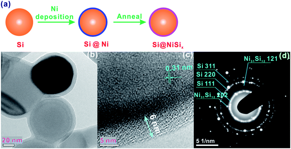 | ||
| Fig. 1 (a) Schematic illustration of coating NiSix on the surface of Si nanoparticles, in which the Si was coated with Ni by sputtering, followed by annealing to allow the Ni to react with the Si, forming the NiSix surface coating, (b) TEM image, (c) HRTEM image, and (d) SAED patterns of Si@6 nm NiSix. | ||
The d-spacing of 0.31 nm shown in Fig. 1c corresponds to the {111} diffraction planes. Because of the poor crystallinity of the coating layer, it is not possible to discern its crystallographics from HRTEM; however, we can identify the {202} and {121} diffraction planes of Ni31Si12 from the selected area electron diffraction (SAED) pattern (Fig. 1c). The energy dispersive X-ray spectroscopy (EDS) mapping indicates the uniform Ni distribution along with Si (Fig. 2a–c), and the EDS line scan confirms the uniform coating (Fig. 2d). Note that we did not observe an elevated Ni content on the edge of Si particle in Fig. 2d, which is likely due to the fact that Ni on the bottom side of Si surface contributes to the EDS signal since the electron beam can reach 1–3 μm in depth during EDS analysis operated at 10 kV and 15 mA. The Ni content in the NiSix-coated Si is ca. 4.12 wt% as suggested by the EDS analysis (Fig. 2e).
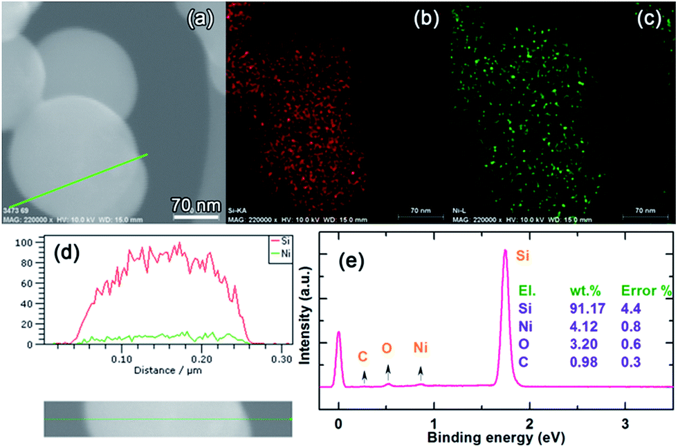 | ||
| Fig. 2 (a) SEM image of Si@6 nm NiSix and its corresponding EDS analysis: elemental mapping of (b) Si-Kα, and (c) Ni-L, (d) line scan of the particle shown in (a), and (e) elemental composition analysis. | ||
Sample Si@6 nm NiSix, for example, was characterized by X-ray photoelectron spectroscopy (XPS) as shown in Fig. 3. The peak centred at 99.9 eV is ascribed to Si in the form of elemental Si and silicide, since their binding energies are too close to be separated. The shoulder peak at 102.4 eV is associated with the surface silicon oxide because Si is prone to oxidation on the surface. The binding energy of the Ni 2p2/3 peak is centred at 853.9 eV, higher than the value belonging to elemental Ni (852.7 eV), but close to those of Ni3Si (852.8 eV), Ni31Si12 (853.0 eV), Ni2Si (853.4 eV), and NiSi (853.9 eV).29,30 This confirms that Ni exists in the form of silicides instead of elemental Ni. No NiO was detected as the O 1s peak of NiO is located at 320 eV, lower than the observed symmetrical peak at 532.4 eV for O 1s in our sample. The O 1s peak was ascribed to oxygen in a form of SiOx because silicon oxide was detected as indicated by the Si 2p peak (102.4 eV).
 | ||
| Fig. 3 XPS spectra of Si@6 nm NiSix, where the peaks were corrected by C 1s at 284.8 eV. | ||
The initial discharge capacity of pristine Si is 2881.3 mA h g−1 at a current density of 120 mA g−1 with an initial Coulombic efficiency (CE) of 90.4% (Fig. 4a). After 50 cycles at the current density of 1200 mA g−1, its capacity was 882.8 mA h g−1, 48.2% of its reversible capacity of 1832.6 mA h g−1 at the third cycle. In contrast, the NiSix coated samples delivered initial capacities of 2214.0, 1985.7, and 2213.4 mA h g−1 with initial CEs of 89.4%, 88.8%, and 89.4% for 1, 4, and 6 nm coating layers, respectively. This means that the introduction of the NiSix coating layer decreased the capacity of the Si anode, e.g., by ca. 23% for sample Si@6 nm NiSix (Fig. 4b), which suggested the existence of the NiSix coating layer because mixing 4.12 wt% of Ni will not decrease the capacity of the Si anode by 23%, whereas the increased polarization by the NiSix will. In other words, it is more difficult for Li+ to cross the NiSix coating layer compared with a conventional SEI layer. Despite the decreased initial capacity, forming a NiSix coating layer significantly enhanced the cyclic performance of the Si anode. As shown in Fig. 4a, the capacities at the 50th cycle are 1237.4, 1123.1, and 1256.0 mA h g−1, 72.3%, 74.9%, and 84.8% of the capacity at the 3rd cycle at 1200 mA g−1 for samples Si@1 nm NiSix, Si@4 nm NiSix, Si@6 nm NiSix, respectively.
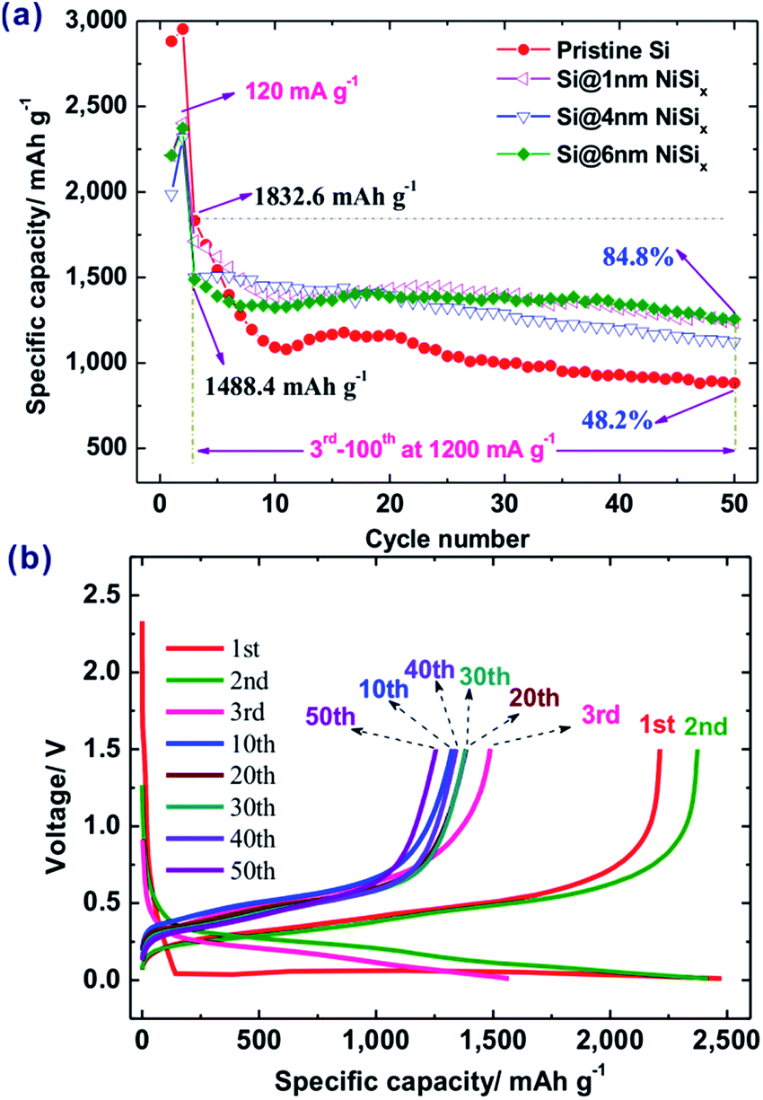 | ||
| Fig. 4 (a) Cyclic performance of pristine Si and NiSix-coated Si with various coating thicknesses, and (b) charge/discharge profiles of sample Si@6 nm NiSix. | ||
As a comparison, we prepared a 6 nm Ni-coated Si without the subsequent heat-treatment; the as-obtained Si@Ni delivered a capacity of 3187.6 mA h g−1 at 120 mA g−1, and retained 51.2% capacity at the 50th cycle at 1200 mA g−1 (Fig. S4†). As a result, while physically coating Ni slightly improved the capacity retention from 48.2% to 51.2%, the chemically bonded silicide surface is much more effective for protecting the Si during cycling, namely, resulting in up to 84.8% of the capacity retention. Note that the Si@Ni possesses a higher capacity than the pristine Si and the silicide-coated Si, which is associated with the fact that Ni metal helps improve the electrical conductivity.
Pure Si usually possesses very poor cyclic performance.13,31,32 For example, Yu et al.13 reported a commercial nanosized Si showing a capacity of ca. 3700 mA h g−1 while decaying to almost zero within 50 cycles. Forming surface coatings on Si was reported to improve the cyclic performance of the Si. For example, Murugesan et al.15 synthesized Cu-coated Si particles by depositing copper on the a-Si:H particles by a polyol-mediated reduction of copper acetate, showing a capacity of ca. 600 mA h g−1 with enhanced cyclic performance. Chen et al.14,21 prepared C-coated and Cu-coated Si nanowire anodes, retaining 75.0% and 86.3%, respectively, of their initial capacities after 15 cycles at 0.05 C rate; in contrast, the pristine Si nanowire anode retained 63.7% of its initial capacity. Considering that very good coating layers were achieved,14 the capacity decay of these coated Si anodes is possibly due to the coating layer breaking and peeling off from the surfaces of the Si nanowires or nanoparticles. As a matter of fact, a broken C coating layer on the SnO2 surface was observed by an in situ TEM.33 As shown in Fig. 5a, taking the Ni-coated Si particle as an example, the coating layer will gradually form cracks and lose electrochemical contact with Si because of the large volume change of Si upon the repeated lithiation/delithiation. Compared with such a physical coating Ni layer serving as a “jacket” layer, our NiSix coating layer was formed by a reaction of the Si surface with the coated Ni; consequently, the as-obtained chemical coating layer acts as a “skin” layer. When the NiSix-coated Si is charged, it may expand and crack somehow, but it will not peel off and lose contact with Si as shown in Fig. 5b.
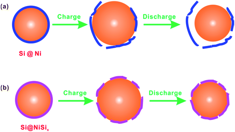 | ||
| Fig. 5 Schematic illustrations of (a) failure mechanism of the conventional coating method, taking Ni-coated Si as an example, and (b) the mechanism for the improved cyclic performance by the formation of the skin-like NiSix on the surface of Si. | ||
Fig. S5† shows SEM images of the Si@6 nm NiSix electrode after 50 cycles; no cracks were observed on the particles, which may be due to the Si particle size smaller than 150 nm, a critical size below which Si would not crack upon lithiation.34 In addition, the SEI layer on the surface of the Si particles may disturb the observation of the nickel silicide coating layer. However, we still can find that the Ni is well distributed on the surface of the Si particle by EDS mapping (Fig. S6†). Note that some big cracks were observed on the electrode (not on the Si particles; Fig. S5†), which can explain why the silicide-coated Si anode still show decay. As a matter of fact, coating an active or inactive layer on the Si particle cannot reduce the volume change of Si upon lithiation, namely, formation of Li3.75Si will anyway lead to the volume expansion of Si up to ∼300%. The strain between the particles due to the repeated expansion and contraction of the Si upon lithiation/delithiation eventually resulted in the cracks on the electrode. Nevertheless, the formation of the silicide coating layer did improve the cyclic performance of the Si anode, as discussed above, because the stable chemically bonded silicide coating layer can prevent the SEI layer from growing upon cycling.
Because sample Si@6 nm NiSix showed the best cyclic performance among the three NiSix coated samples, we took this sample as an example to investigate the mechanism of the improved cyclic performance. Fig. 6a shows CV curves of sample Si@6 nm NiSix, recorded at a scan rate of 0.05 mV s−1. During the initial cathodic scan, a current peak emerged at 0.19 V, followed by another developmental peak below 10 mV, corresponding with lithiation of Si to various LixSi phases. When potentials were swept anodically, there were two peaks at 0.36 and 0.51 V due to the delithiation of the LixSi. The CV behaviour is very similar to our previously reported Si/Ni composite.29 Note also that the gradual development of cathodic and anodic peaks was commonly observed in CV curves of Si anodes,35–37 which is due to the gradual activation of Si.
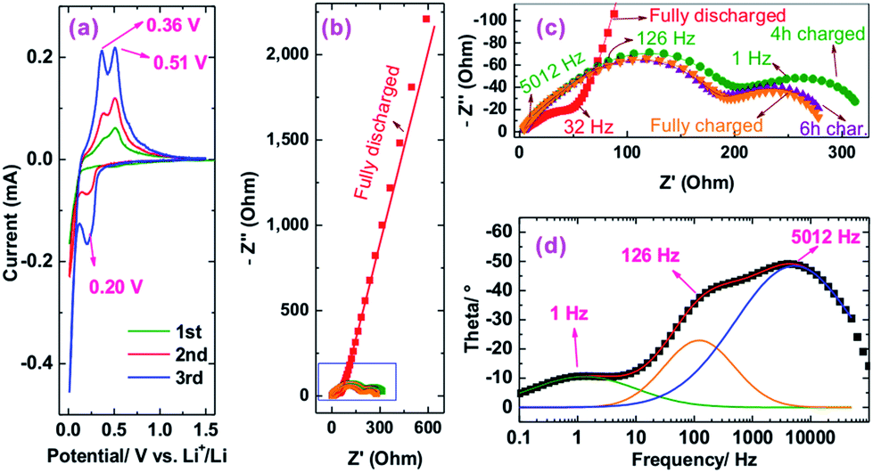 | ||
| Fig. 6 (a) CV curves, (b and c) Nyquist plots at various states of charge, in which discrete points and solid lines represent the experimental data and the fitting results, and (d) Bode plot (discrete points) and their peak fitting results (solid lines). Note that the three highest-frequency points were removed during fitting because they are not very stable; including the three points will increase the fitting error significantly. | ||
Fig. 6b and c shows the electrochemical impedance spectroscopy (EIS) Nyquist plots of the NiSix-coated Si anode. To reach a fully charged state, the anode was charged to 1.5 V and maintained at 1.5 V for 1 h. After allowing the anode to rest for 1 h, the anode was measured by EIS; its Nyquist plot exhibits a semicircle at the high frequency zone, followed by an inclined line after ca. 32 Hz. The semicircle represents only the resistance of the SEI layer without charge transfer resistance because the potential of the anode is 1.461 V, far away from the lithiation/delithiation potentials as indicated by the CV (Fig. 6a). The inclined line should be related to the diffusion of Li ions in the SEI layer instead of in the bulk of Si particles. This is in good agreement with our recent results on a Si/Ni composite29 and a Si flower anode.38
The NiSix coated Si anode was subsequently charged at 240 mA g−1 (C/10) for various durations to obtain its charge transfer resistance. After charging, apparently, there are two semicircles in the Nyquist plots (Fig. 6c); however, when we analysed the Bode plot, taking the 4 h charged state as an example, we found three peaks located at ca. 5012, 126, and 1 Hz (Fig. 6d), which are associated with the SEI layer, the NiSix coating layer, and the charge transfer, respectively. We therefore used a three time-constant equivalent circuit (Fig. S7†) to fit the Nyquist plots and summarized the results in Table S1.† Considering the resistances are typically stable at or near a half charged state,38 we averaged the resistances obtained at the 4 h and 6 h charged states, which shows that the Ohmic (including electrolyte and contact resistances), SEI layer, NiSix coating layer, and charge transfer resistances are 3.0, 40.0, 150.3, and 115.2 Ohm, respectively.
Compared with our previous Si/Ni composite with the resistances of the SEI layer and the charge transfer of 60.0 and 139.5 Ohm, respectively,29 the present NiSix-coated Si showed an extra NiSix coating layer resistance (150.3 Ohm). Note that the capacities at 1200 mA g−1 at the 3rd cycles are 71.2%, 64.7%, and 62.7% of the values obtained at 120 mA g−1 at the 2nd cycles for samples Si@1 nm NiSix, Si@4 nm NiSix, and Si@6 nm NiSix, respectively (Fig. 4a), which means that the rate capabilities of the NiSix-coated Si anode decreased with the increasing coating thickness. Therefore, forming a thinner NiSix coating layer, e.g., by the ALD technique, may lead to less capacity loss while enhancing the cyclic performance of Si anodes. Although forming a NiSix coating layer may increase the resistance and decrease the capacity, it can significantly improve the cyclic performance. Because Si possesses a theoretical capacity of 3579 mA h g−1, approximately ten times that of commercial graphite anodes, it is worth improving its cyclic performance at the cost of a decreasing capacity. As a result, the formation of the NiSix coating layer like we designed here offers a new approach to improve the cyclic performance of Si anodes.
In conclusion, NiSix-coated Si was synthesized by sputtering Ni on the surface of Si particles, followed by annealing at 800 °C. The sputtered Ni reacted with the surface of the Si, forming a NiSix intermetallic coating layer. Compared with the pristine Si losing 51.8% of its reversible capacity within 50 cycles, the NiSix-coated Si with a 6 nm coating layer retained 84.8% of its reversible capacity. The improved cyclic performance is related to strong binding of the skin-like NiSix to the Si surface due to the chemical bonding, in contrast to relatively weak binding for a physically coated layer on Si.
Acknowledgements
Financial support for this work was provided by the U.S. Department of Energy (DE-EE0003208) and Johnson Controls, Inc. The SEM imaging was conducted at the UWM Bioscience Electron Microscope Facility, and TEM analyses were conducted in the UWM Physics HRTEM Laboratory. The authors thank Dr H. A. Owen, Dr S. E. Hardcastle and D. P. Robertson for their technical support with SEM, BET and Raman, and TEM analysis, respectively.Notes and references
- U. Kasavajjula, C. S. Wang and A. J. Appleby, J. Power Sources, 2007, 163, 1003–1039 CrossRef CAS PubMed.
- E. M. Lotfabad, P. Kalisvaart, K. Cui, A. Kohandehghan, M. Kupsta, B. Olsen and D. Mitlin, Phys. Chem. Chem. Phys., 2013, 15, 13646–13657 RSC.
- B. J. Jeon and J. K. Lee, Electrochim. Acta, 2011, 56, 6261–6265 CrossRef CAS PubMed.
- B. E. Kim, S. E. Park, J. C. Lim and J. K. Lee, Phys. Scr., 2010, 139, 014021 CrossRef.
- O. Park, J. I. Lee, M. J. Chun, J. T. Yeon, S. Yoo, S. Choi, N. S. Choi and S. Park, RSC Adv., 2013, 3, 2538–2542 RSC.
- Y. He, X. Q. Yu, Y. H. Wang, H. Li and X. J. Huang, Adv. Mater., 2011, 23, 4938–4941 CrossRef CAS PubMed.
- H. T. Nguyen, M. R. Zamfir, L. D. Duong, Y. H. Lee, P. Bondavalli and D. Pribat, J. Mater. Chem., 2012, 22, 24618–24626 RSC.
- J. C. Li, X. C. Xiao, Y. T. Cheng and M. W. Verbrugge, J. Phys. Chem. Lett., 2013, 4, 3387–3391 CrossRef CAS.
- Y. M. Kang, S. M. Lee, M. S. Sung, G. J. Jeong, J. S. Kim and S. S. Kim, Electrochim. Acta, 2006, 52, 450–454 CrossRef CAS PubMed.
- Y. Hwa, W. S. Kim, B. C. Yu, S. H. Hong and H. J. Sohn, J. Phys. Chem. C, 2013, 117, 7013–7017 CAS.
- H. Usui, Y. Kashiwa, T. Iida and H. Sakaguchi, J. Power Sources, 2010, 195, 3649–3654 CrossRef CAS PubMed.
- E. L. Memarzadeh, W. P. Kalisvaart, A. Kohandehghan, B. Zahiri, C. M. B. Holt and D. Mitlin, J. Mater. Chem., 2012, 22, 6655–6668 RSC.
- Y. Yu, L. Gu, C. B. Zhu, S. Tsukimoto, P. A. van Aken and J. Maier, Adv. Mater., 2010, 22, 2247–2250 CrossRef CAS PubMed.
- H. X. Chen, Y. Xiao, L. Wang and Y. Yang, J. Power Sources, 2011, 196, 6657–6662 CrossRef CAS PubMed.
- S. Murugesan, J. T. Harris, B. A. Korgel and K. J. Stevenson, Chem. Mater., 2012, 24, 1306–1315 CrossRef CAS.
- V. A. Sethuraman, K. Kowolik and V. Srinivasan, J. Power Sources, 2011, 196, 393–398 CrossRef CAS PubMed.
- H. Usui, N. Uchida and H. Sakaguchi, J. Power Sources, 2011, 196, 10244–10248 CrossRef CAS PubMed.
- W. Wang, M. Tian, Y. J. Wei, S. H. Lee, Y. C. Lee and R. G. Yang, Nano Energy, 2013, 2, 943–950 CrossRef CAS PubMed.
- C. Y. Du, M. Chen, L. Wang and G. P. Yin, J. Mater. Chem., 2011, 21, 15692–15697 RSC.
- S. H. Ng, J. Wang, D. Wexler, S. Y. Chew and H. K. Liu, J. Phys. Chem. C, 2007, 111, 11131–11138 CAS.
- H. X. Chen, Z. X. Dong, Y. P. Fu and Y. Yang, J. Solid State Electrochem., 2010, 14, 1829–1834 CrossRef CAS PubMed.
- Y. Yao, N. Liu, M. T. McDowell, M. Pasta and Y. Cui, Energy Environ. Sci., 2012, 5, 7927–7930 CAS.
- H. S. La, K. S. Park, K. S. Nahm, K. K. Jeong and Y. S. Lee, Colloids Surf., A, 2006, 272, 22–26 CrossRef CAS PubMed.
- A. A. Arie, W. Chang and J. K. Lee, J. Solid State Electrochem., 2010, 14, 51–56 CrossRef CAS.
- X. H. Liu and J. Y. Huang, Energy Environ. Sci., 2011, 4, 3844–3860 CAS.
- M. S. Park, S. Rajendran, Y. M. Kang, K. S. Han, Y. S. Han and J. Y. Lee, J. Power Sources, 2006, 158, 650–653 CrossRef CAS PubMed.
- T. Kim, S. Park and S. M. Oh, Electrochem. Commun., 2006, 8, 1461–1467 CrossRef CAS PubMed.
- H. X. Chen, Q. B. Zhang, J. X. Wang, D. G. Xu, X. H. Li, Y. Yang and K. L. Zhang, J. Mater. Chem. A, 2014, 2, 8483–8490 CAS.
- X. K. Huang, H. H. Pu, J. B. Chang, S. M. Cui, P. B. Hallac, J. W. Jiang, P. T. Hurley and J. H. Chen, ACS Appl. Mater. Interfaces, 2013, 5, 11965–11970 CAS.
- Y. Cao, L. Nyborg and U. Jelvestam, Surf. Interface Anal., 2009, 41, 471–483 CrossRef CAS PubMed.
- H. M. Jeong, S. Y. Lee, W. H. Shin, J. H. Kwon, A. Shakoor, T. H. Hwang, S. Y. Kim, B. S. Kong, J. S. Seo, Y. M. Lee, J. K. Kang and J. W. Choi, RSC Adv., 2012, 2, 4311–4317 RSC.
- X. S. Zhou, Y. X. Yin, L. J. Wan and Y. G. Guo, Chem. Commun., 2012, 48, 2198–2200 RSC.
- L. Q. Zhang, X. H. Liu, Y. Liu, S. Huang, T. Zhu, L. J. Gui, S. X. Mao, Z. Z. Ye, C. M. Wang, J. P. Sullivan and J. Y. Huang, ACS Nano, 2011, 5, 4800–4809 CrossRef CAS PubMed.
- X. H. Liu, L. Zhong, S. Huang, S. X. Mao, T. Zhu and J. Y. Huang, ACS Nano, 2012, 6, 1522–1531 CrossRef CAS PubMed.
- C. K. Chan, H. L. Peng, G. Liu, K. McIlwrath, X. F. Zhang, R. A. Huggins and Y. Cui, Nat. Nanotechnol., 2008, 3, 31–35 CrossRef CAS PubMed.
- Y. Zhao, X. Z. Liu, H. Q. Li, T. Y. Zhai and H. S. Zhou, Chem. Commun., 2012, 48, 5079–5081 RSC.
- T. Jiang, S. C. Zhang, X. P. Qiu, W. T. Zhu and L. Q. Chen, Electrochem. Commun., 2007, 9, 930–934 CrossRef CAS PubMed.
- X. Huang, J. Yang, S. Mao, J. Chang, P. B. Hallac, C. R. Fell, B. Metz, J. Jiang, P. T. Hurley and J. Chen, Adv. Mater., 2014, 26, 4326–4332 CrossRef CAS PubMed.
Footnote |
| † Electronic supplementary information (ESI) available. See DOI: 10.1039/c5ra00764j |
| This journal is © The Royal Society of Chemistry 2015 |