
Bottom-up growth of Ag/a-Si@Ag arrays on silicon as a surface-enhanced Raman scattering substrate with high sensitivity and large-area uniformity†
Liwei Liua,
Mingliang Jinb,
Qingwei Zhoua,
Runze Zhanc,
Huanjun Chenc,
Xingsen Gaoa,
Stephan Senzd,
Zhang Zhang*a and
Junming Liu*e
aInstitute for Advanced Materials, Laboratory of Quantum Engineering and Quantum Materials, South China Academy of Advanced Optoelectronics, South China Normal University, Guangzhou 510006, People's Republic of China. E-mail: zzhang@scnu.edu.cn
bElectronic Paper Display Institute, South China Academy of Advanced Optoelectronics, South China Normal University, Guangzhou 510006, People's Republic of China
cState Key Laboratory of Optoelectronic Materials and Technologies, Guangdong Province Key Laboratory of Display Material and Technology, School of Physics and Engineering, Sun Yat-sen University, Guangzhou 510275, People's Republic of China
dMax Plank Institute of Microstructure Physics, Weinberg 2, Halle 06120, Germany
eLaboratory of Solid State Microstructures, Nanjing University, Nanjing 210093, China. E-mail: liujm@nju.edu.cn
First published on 10th February 2015
Abstract
In this work, we demonstrated a bottom-up growth of Ag/a-Si@Ag nanosphere arrays on Si to work as a high performance SERS substrate. By a solid-state dewetting process, high density Ag nanoparticle arrays were formed on the Si substrate with large-area uniformity. With well-controlled thicknesses of a-Si and Ag outer-layer coating, the SERS properties can be optimized with the inter-particle spacing of the Ag/a-Si@Ag NSs limited to several nanometers. Based on the analysis of optical properties and SERS activities to p-Tc molecules, we concluded that the optimized SERS substrate performed with both high sensitivity and large-area uniformity. A detection limit as low as 10−14 M and an enhancement factor (EF) up to 108 were obtained. Furthermore, the wafer scale large-area uniformity and reproducibility of the SERS signal were confirmed with small standard deviation, e.g., 8% at 1076 cm−1 and 9% at 1593 cm−1. The generic approach presented here can be extended to create a new class of highly sensitive SERS sensors with large-area output, and may play an important role in device design and the corresponding diverse chemical and biological detection tasks.
Introduction
Surface-enhanced Raman scattering (SERS), one of the most powerful and promising techniques, has been widely used in a variety of applications due to its high sensitivity, excellent selectivity, and rapid detection capability.1 SERS effects are usually found in adjacent noble metallic nanostructures that are called “hot spots”, where electromagnetic fields are largely enhanced. Recent studies have shown that “hot spots” have a large contribution to enormous Raman signal enhancement,2,3 allowing rapid detection of Raman signals and highly sensitive identification of single molecules.4,5Numerous approaches have been widely investigated for the design of diverse noble metallic nanostructures as SERS substrates, which can be classified into wet and dry methods or bottom-up and top-down methods. For the wet methods, substrates based on metal colloids stabilizations have been reported to achieve a SERS enhancement with a high sensitivity.6,7 In order to realize a stable solid SERS substrate with large-area uniformity, patterning of “hot spots” via dry methods had been developed, such as nanospheres (NSs) lithography,8,9 reactive ion etching (RIE),10 electron-beam lithography (EBL),11 and nano-imprint lithography.12 Typically, the top-down methods are time-consuming with a high fabrication cost. Besides, to control the feature size of “hot spots” into the sub-10 nm regime to enhance SERS signal, approaches based on the bottom-up methods have been extensively exploited. Ordered arrays of Ag nanoparticles (NPs) had been grown in porous anodic aluminum oxide (AAO) templates with tunable sub-10 nm inter-particle gaps.13 Self-assembling of polystyrene (PS) spheres is a feasible choice instead of AAO with a pre-etching, which has a good control over the inter-particle gaps.14–16 However, the PS spheres are usually several hundred nanometers in diameter, which reduces the density of “hot spots” under the Raman laser spot resulting in a limited sensitivity of SERS substrate.
Recently, substrate-supported metallic nanoparticle arrays have been fabricated over a large area by a solid-state dewetting, which attracted considerable interest for applications in solar cells, plasmonics and chemical etching.17–19 In particular, SERS substrate is one of the most important applications of substrate-supported metallic nanoparticle arrays with large-area uniformity.20 For example, one feasible SERS substrate of double-layer stacked Au/Al2O3@Au nanosphere arrays was realized on Si wafer.21 However, applying a simple annealing process, the inter-particle spacing of nanoparticles were too large to work efficiently as “hot spots”. Both theoretical and experimental data demonstrated that an inter-particle gap of less than 5 nm was essential for strong enhancement of Raman signals.22,23 Therefore, to meet the requirements of high quality SERS substrate, much effort need to be put on tailoring the inter-particle spacing of substrate-supported metallic nanoparticle arrays.
In this paper, we present a bottom-up method to realize Ag/a-Si@Ag nanosphere arrays on Si as a SERS substrate with high sensitivity and large-area uniformity. Via a solid-state dewetting, high density Ag nanoparticle arrays were formed on Si substrate with large-area uniformity. By a chemical vapor deposition (CVD), a-Si grew homogeneously on the surfaces of Ag NPs and Si substrate in between. With a controlled thickness of a-Si and Ag out-layer coating, we demonstrated that the inter-particle spacing of the Ag/a-Si@Ag nanosphere arrays could be reduced to several nanometers to work as a SERS substrate. Through a study on their optical properties and SERS activities, the self-assembly bottom-up growth of Ag/a-Si@Ag nanosphere arrays as a SRES substrate exhibits high sensitivity of 10−14 M and large-area uniformity.
Experimental
Sample preparation
The n-doped Si(111) wafers were prepared by a standard RCA cleaning, and then dipped into 5% hydrofluoric acid to have a silicon oxide removed and obtain a hydrogen-terminated Si surface. A thin Ag film with a 15 nm thickness was deposited by a thermal evaporation process at a growth rate of 0.1 Å s−1. Subsequently, the substrate was loaded to a LP-CVD system (firstnano ET-3000 EXT, CVD Equipment Corp.), and was heated up to 540 °C for 30 min at 10 Torr pressure to form Ag nanoparticle arrays. The Ag/a-Si NSs were synthesized by a CVD process with diluted silane (5% SiH4 in H2) as gas precursor and 99.999% pure H2 as carrier gas. The pressure was set to be 10 Torr with a fixed mass flow of 40 sccm H2, 20 sccm SiH4. The growth time of Si layer was 30, 60, 90 min, respectively. Finally, an out-layer of Ag with thickness from 5 nm, 10 nm, 15 nm, 20 nm, 25 nm to 30 nm was coated onto the Ag/a-Si NSs to form a SERS substrate. The nanostructures were characterized by SEM (ZEISS Ultra 55), TEM (JEOL JEM-2100HR), and AFM (Cypher™, Asylum Research). Ultraviolet-visible (UV-vis) mirror reflection spectra were obtained by a SpectraSuite (Ocean Optics HR4000).SERS detection
For the measurement of SERS, all the vibration experiments were carried out with 633 nm excitation laser lines. The inelastic scattered radiation was collected on a microscopy Raman spectrometer (Renishaw 42K864) with a CCD detector and an optical microscope using a 50× microscope objective with a numerical aperture (NA) value of 0.50. Regarding the SERS measurements, the analyte molecules p-Tc at different concentrations, ranging from 0.4 mM to 10−14 M were prepared in ethanol solutions. For the 0.4 mM the substrates were dipped into a solution of molecules dissolved in ethanol for 1 h, then washed in ethanol to remove excess molecules and dried in the air. For the measurements at lower concentrations (from 10−10 M to 10−14 M), the substrates were dipped into solutions for 1 hour, then were immersed into an de-ionized water for 5 hours to remove the adsorbed ethanol that attached to the metal surface, followed by drying in the air. All the samples were soaked into identical bottles containing p-Tc (from 4 × 10⁻⁴ M to 1 × 10⁻¹⁴ M, 50 ml).Results and discussion
Fabrication procedures
The fabrication procedures of Ag/a-Si@Ag nanosphere arrays are illustrated schematically in Fig. 1. First, a thin Ag film with a thickness of 15 nm was deposited on Si(111) substrate via a high vacuum thermal evaporation (Fig. 1a). Ag nanoparticle arrays were formed by an annealing at 540 °C in the CVD chamber (Fig. 1b). In general, with a lower annealing temperature and a shorter annealing time, a higher density of metal nanoparticle arrays was achieved.24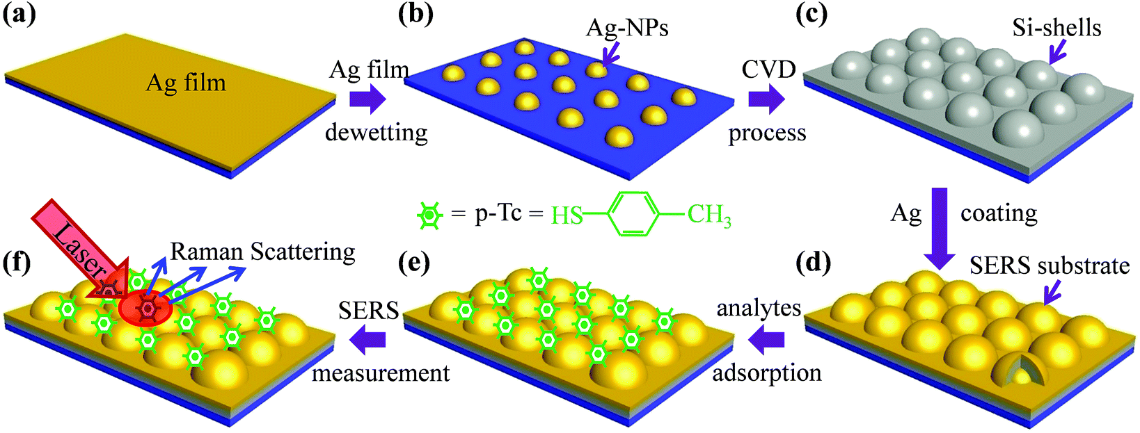 | ||
| Fig. 1 Schematic diagrams to illustrate the fabrication procedures of Ag/a-Si@Ag nanosphere arrays on Si substrate as a SERS substrate to detect probed molecules, such as p-thiocresol (p-Tc). | ||
After annealing, a reactive gas precursor of SiH4 (5%) mixed with a carrier gas of H2 were fluxed into the CVD chamber. With SiH4 decomposed on the hot surfaces, Si atoms homogeneously deposited on surfaces of Ag NPs and Si substrate in between. Depictured in Fig. 1c, a-Si layer covered on the Si substrate homogeneously with embedded Ag NPs. The CVD growth of a-Si layer further reduced the inter-particle spacing of Ag NPs. Meanwhile, the continuously grown a-Si immobilized the Ag NPs from further agglomeration. Then, an outer layer of Ag covered onto the a-Si by thermal evaporation to form Ag/a-Si@Ag nanosphere arrays (Fig. 1d), which can work as SERS substrate. p-Thiocresol (p-Tc), a kind of nonfluorescent molecule, was trapped on the gaps of Ag/a-Si@Ag nanosphere arrays by chemisorption of molecules dissolved ethanol solution (as illustrated in Fig. 1e). In terms of SERS signals, the excitation laser was used to interact with the trapped p-Tc molecules to characterize the Ag/a-Si@Ag nanosphere arrays as a SERS substrate (Fig. 1f).
Characterization of Ag/a-Si@Ag nanosphere arrays
In order to maximize the density of “hot spots”, morphologies of tunable growth of Ag/a-Si@Ag nanosphere arrays on Si substrate are shown in scanning electron microscopy (SEM) images in Fig. 2. In top view (Fig. 2a) and 75°-tilt view (Fig. 2b) SEM images, we confirmed that, the 15 nm solid-state Ag film on Si had dewetted into Ag nanoparticle arrays of high density and large-area uniformity. Inter-particle spacing between the Ag NPs was tunable with different annealing time under a given temperature (Fig. S1†). The inset of Fig. 2b illustrates the size distribution of about 550 Ag NPS, and the mean diameter is about 73 nm. However, after a direct heating up to 540 °C for 30 min without annealing, most of the inter-particle spacing was larger than 100 nm. In order to control the inter-particle spacing into several nanometer regime as “hot spots” for an effective SERS substrate, an a-Si layer was grown on Ag NPs via a CVD process. Fig. 2c displays a SEM image of Ag/a-Si nanosphere arrays after a 90 min CVD growth of Si. The Ag/a-Si nanosphere arrays on Si substrate are closely packed, and most of the gaps between adjacent Ag/a-Si nanospheres shrink to sub-10 nm. The cores of Ag/a-Si nanospheres with a bright contrast (under a high electron acceleration voltage of 15 kV) in Fig. 2c represent the Ag NPs embedded in the a-Si layer of about 50 nm thick with a dark contrast. The inset shows Raman spectra of Si substrate before (red line) and after (blue line) the CVD growth of Si. In the Raman spectra, the sharp peak at 521 cm−1 indicates the crystalline Si(111) substrate. Apart from the strong band at 521 cm−1, the additional board band at 480 cm−1 represents the growth of amorphous a-Si.25 Fig. 2d shows a 75°-tilt view SEM image of Ag/a-Si nanosphere arrays. The inset of Fig. 2d illustrates the size distribution of about 350 Ag/a-Si NSs with a mean diameter of about 170 nm, from which the mean size of Ag nanoparticle core was estimated to be 70 nm in diameter without further agglomeration during Si growth. Top view (Fig. 2e) and 75°-tilt view (Fig. 2f) SEM images illustrate Ag/a-Si@Ag nanosphere arrays as a SERS substrate after a 15 nm thick Ag out-layer coating. The Ag coating thickness was optimized to achieve the strongest SERS signals, which resulted to be 15 nm at a laser excitation wavelength of 633 nm. The inset of Fig. 2f illustrates the size distribution histograms of the Ag/a-Si@Ag nanosphere arrays. After the Ag out-layer coating, there exists a systematic increase in the size of Ag/a-Si@Ag nanospheres with the mean diameter of 190 nm, which is in accord with the thickness of Ag coating shown in Fig. 2e. | ||
| Fig. 2 Top-view SEM image (a) and 75° tilted-view SEM image (b) of Ag nanoparticles (NPs), inset shows the size distribution histogram of diameters of Ag NPs. (c) Top-view SEM image of Ag/a-Si nanosphere arrays, inset shows Raman shifts of Si substrate before (red line) and after (green line) CVD process. (d) 75° tilted-view SEM image of Ag/a-Si nanosphere arrays with a 90 min Si CVD growth and inset of (d) is the corresponding size distribution histogram. (e) Top-view SEM image Ag/a-Si@Ag nanosphere arrays as SERS substrate. (f) 75° tilted-view SEM image Ag/a-Si@Ag nanosphere arrays with a 15 nm thick Ag out-layer, inset shows the corresponding size distribution histogram of diameters of Ag/a-Si@Ag NSs. | ||
Crystallographic characterizations are shown in transmission electron microscopy (TEM) images of Fig. 3. Cross-sectional nanostructure of Ag/a-Si nanosphere arrays grown on Si(111) substrate is shown in Fig. 3a. After the CVD growth, an a-Si layer with a uniform thickness of 50 nm covered the surfaces of both Ag NPs and Si substrate in between. The gaps between Ag/a-Si nanospheres (NSs) on Si substrate are decided by the thicknesses of the a-Si layer, which could be adjusted by different growth time at a certain growth temperature (see Fig. S3†). A fine-grained Ag film was deposited onto the surfaces of Ag/a-Si nanosphere arrays, as shown in the cross-sectional image of Fig. 3b. From the magnified cross-sectional TEM image of an individual Ag/a-Si@Ag nanosphere (shown in Fig. 3c), we measured that the thickness of Ag film was about 15 nm. Moreover, high resolution TEM images (Fig. 3d and e) were acquired from different regions marked by the red dotted line boxes plotted in Fig. 3c. The single crystalline nature of Si(111) substrate was confirmed by the FFT pattern of Si substrate (inset of Fig. 3d). And the a-Si was grown on the Si substrate covered by a thin Si oxides layer with a thickness around 1 nm, which is consistent with the Raman peak at 480 cm−1 observed in Fig. 2c. Upon a closer inspection of Fig. 3e at the interface of Ag and a-Si, the lined fringes indicated the crystalline nature of Ag NPs after the CVD growth, which is further confirmed by the selected area electron diffraction (SAED) pattern taken from Ag/a-Si NSs being a face-centered cubic (fcc) crystal structure (see Fig. S4†).
 | ||
| Fig. 3 Cross-sectional TEM images of (a) Ag/a-Si nanosphere arrays and (b) Ag/a-Si@Ag nanosphere arrays with Ag film coating both on Si(111) substrates, the a-Si layer is about 50 nm thick. (c) Magnified cross-sectional TEM image of a single Ag/a-Si@Ag nanosphere on the Si substrate, the thickness of Ag coating is about 15 nm. (d) HRTEM image taken from the selected area marked in (c) of Ag/a-Si@Ag nanosphere with the corresponding FFT pattern as inset, which illustrates the amorphous a-Si growth on the single-crystalline Si(111) substrate with a thin SiO2 interface. (e) HRTEM image taken from the selected area marked in (c) with the crystalline Ag core surrounded by the a-Si shell. | ||
Optical response
Optical properties of nanostructures at different stages: (i) Ag film deposition; (ii) dewetted Ag NPs; (iii) Ag/a-Si nanosphere arrays were characterized by a UV-vis reflection spectroscopy in Fig. 4a. The Si substrate with the continuous Ag film has a higher reflectance than the one with Ag nanoparticle arrays after dewetting. Moreover, the Ag nanoparticle arrays on Si exhibit a distinct plasmonic reflection trough at 450 nm, which is consistent with literature.26 After the Si growth, the reflection trough red-shifts to 617 nm related to the nanostructure of a-Si layer embedding Ag NPs. Furthermore, UV-vis reflection spectra of Ag/a-Si@Ag nanosphere arrays with different Ag out-layer coating thicknesses are displayed in offset y values form (shown in Fig. 4b). With the Ag coating thickness increased from 5 nm to 10 nm, the corresponding UV-vis spectra exhibit an obvious red shift from 622 nm to 643 nm. The red shift is mainly related to the increase of the size of discrete small Ag NPs composing the Ag out-layer,18 which was observed in top-view SEM images (see Fig. S5a and b†). The reflection spectrum of Ag/a-Si@Ag nanosphere arrays with a 15 nm thick Ag coating has a blue shift to 627 nm, which may be attributed to transformation of the discrete Ag NPs into connected nanoislands. Typically, as the wavelength of the excitation laser in Raman being in accordance with the position of reflection trough, Raman signals were found to be more obvious.27 Since the wavelength of the excitation laser in our Raman characterizations is 633 nm, the blue shift to 627 nm with a 15 nm thick Ag coating has a better coupling between the incident light and surface plasmonic polarizations, resulting in stronger Raman signals. However, with increasing the Ag coating thickness, the reflection trough tends to disappear and would give weak Raman signals. Therefore, for Ag/a-Si@Ag nanosphere arrays on Si as a SERS substrate, the Ag coating with a thickness of 15 nm was confirmed to be optimized with the 633 nm excitation wavelength. | ||
| Fig. 4 (a) UV-vis reflection spectra with different fabrication stages of Ag/a-Si@Ag nanosphere arrays on Si substrate: (i) Ag film deposition, (ii) solid-state dewetting of Ag NPs, (iii) Ag/a-Si nanosphere arrays formation. (b) Reflection spectra of Ag/a-Si@Ag nanosphere arrays on Si substrate with the Ag out-layer coating thicknesses varying from 5 nm to 25 nm. | ||
SERS characterization
To study the direct influence of Ag coating thickness on the SERS performance, after the chemisorption in a 0.4 mM p-Tc solution, Raman spectra of Ag/a-Si@Ag nanosphere arrays with different Ag coating thicknesses are compared. All the spectra show clear Raman peaks of p-Tc (see Fig. S6a†). The intensities of Raman peaks at 1076 cm−1 with different Ag coating thicknesses are shown statistically in the bar chart of Fig. 5a, in which the strongest Raman signals are observed on the SERS substrate with the 15 nm thick Ag coating. However, the rough nanostructures of the Ag film coating on a plane Si substrate with the same depositing conditions also have a SERS effect. In order to identify that the SERS effect is mainly from the Ag/a-Si@Ag nanosphere arrays, Raman spectra from the Ag/a-Si@Ag nanosphere arrays are compared with the ones obtained on plane Si substrates with the same Ag coating thicknesses (see Fig. S6b†). It is evident that the SERS effect from the Ag film coating on a-Si layer is negligible. For a practical application, we compares the average Raman spectra intensity of analyte p-Tc chemisorbed on the Ag/a-Si@Ag nanosphere arrays with that obtained on a commercial Klarite SERS substrate. As shown in Fig. 5b, the strongest Raman peaks at 1076 and 1593 cm−1 belonging to p-Tc are observed on both SERS substrates.28 The peak at 1076 cm−1 is due to a combination of phenyl ring-breathing mode, CH in-plane bending, and CS stretching, while the peak at 1593 cm−1 can be assigned to phenyl stretching motion.29,30 With the optimized thickness of Ag out-layer coating, the intensity of Raman peak at 1076 cm−1 from the Ag/a-Si@Ag nanosphere arrays is 15 times stronger than the one from the commercial SERS substrate. | ||
| Fig. 5 (a) Raman intensities of p-Tc at 1076 cm−1 peak with different Ag coating thicknesses (5 nm to 30 nm). (b) Comparison of Raman spectra of p-Tc chemisorbed on the Ag/a-Si@Ag SERS substrate with the commercial SERS substrate and bare Ag/a-Si NSs. (c) Raman spectra of the Ag/a-Si@Ag SERS substrate with p-Tc concentrations ranging from 10−10 M to 10−14 M, and a plane SERS substrate with p-Tc concentration of 10−6 M. (d) An enlarged view of Raman spectra obtained from Ag/a-Si@Ag SERS substrate (10−13 M p-Tc) and from the plane SERS substrate (10−6 M p-Tc) at 1076 cm−1 peak. | ||
In order to confirm the Ag/a-Si@Ag nanosphere arrays on Si as a SERS substrate has a high sensitivity, Raman spectra from the SERS substrates with different p-TC concentrations (from 10−10 to 10−14 M) are shown in Fig. 5c. With the p-Tc concentration decreasing, typical Raman peaks of p-TC can be clearly identified down to a p-Tc concentration of 10−13 M. Even with a 10−14 M concentration, the Raman peaks at 623 cm−1 and 1593 cm−1 are still distinguished from background. Compared with the double-layer stacked Au/Al2O3@Au nanosphere structures enabling a sensitivity down to 10−9 M,21 obviously, the SERS substrate based on the Ag/a-Si@Ag nanosphere arrays has a much higher sensitivity. However, on a plane Si substrate coated with Ag film of the identical thickness, the detection limit of p-Tc is only 10−6 M (see Fig. S7†). Therefore, the observed high sensitivity of 10−14 M is attributed to the Ag/a-Si@Ag nanosphere arrays. Due to a coupling of the localized surface plasmon resonances (LSPR), the electrical field of the adjacent nanospheres could be enhanced by more than 108 folds.31,32 The finite difference time-domain (FDTD) method was used to simulate the near-filed electrical field distribution in a model of two Ag/a-Si@Ag NSs with different inter-sphere gaps (from 5 nm to 20 nm). The calculation confirmed that the coupling of LSPR was generated in the vicinity of the gap region and decayed rapidly outside the gap (see Fig. S8†).
In order to estimate the enhancement factor (EF) of the Ag/a-Si@Ag nanosphere arrays on Si as a SERS substrate, two methods were carried out.33,34 One estimation was based on the FDTD simulation, and the total SERS EF was calculated to be 3.11 × 10⁷ (see corresponding calculations in the ESI with Fig. S8 and S9†). Since this value varies significantly depending on the initial assumptions, we compared with the other estimation, which came directly from the comparison of the Raman spectra of p-Tc obtained on the Ag/a-Si@Ag nanosphere arrays with the one on a planar SERS substrate (as the reference). Considering the formula of EF = (ISERS/Iref)/(CSERS/Cref), CSERS and Cref correspond to the concentrations of the p-Tc molecules in the SERS (10−13 M) and the reference (10−6 M), respectively. ISERS and Iref denote the corresponding average intensities of the 1076 cm−1 Raman peak (shown in Fig. 5d), respectively. Therefore, the total SERS EF was estimated to be 2.22 × 10⁸.
Fig. 6a illustrates 2.5 cm × 5 cm cut Si wafers with the growth of Ag/a-Si nanosphere arrays and with the growth of Ag/a-Si@Ag nanosphere arrays, respectively. After Ag film coating, the wafer changed colour from blue (up) to grey-blue (down). The large-area uniformity of Ag/a-Si@Ag nanosphere arrays on Si was further supported by the atomic force micrograph (AFM) characterization. Fig. 6b displays AFM topography of a randomly selected area on the SERS substrate. A uniform distribution of Ag/a-Si@Ag NSs is seen over a 10 μm × 10 μm areas on the Si substrate. Besides the large-area uniformity in nanostructure, the good reproducibility of SERS signals across the wafer was also tested. The point by point scanning mode was carried out using a laser spot diameter of 1.54 μm (×50 objective lens with NA = 0.5) and a step-size of 100 μm (inset in Fig. 6a). Fig. 6c demonstrates the 3D waterfall plot of enhanced Raman spectra obtained from 10 locations (along arrow marked in the inset of Fig. 6a), displaying almost the same intensity for each characteristic p-Tc peak. Raman intensities at 1076 cm−1 peak from 10 × 10 locations (inset in Fig. 6a) were then plotted to a planar Raman map of enhancement. The Raman map in Fig. 6d suggested that most of the Raman intensities of the 1076 cm−1 peak are in 6800–7800 a.u. range (blue color). According to the statistical analysis of Raman peak at 1076 cm−1 and 1593 cm−1 (Fig. S10†), the calculated relative standard deviation (RSD) of the Raman intensity is 8% and 9%, which prove strongly the reproducibility of the SERS substrate.35 The RSD less than 10% demonstrated that the Ag/a-Si@Ag nanosphere arrays on Si was suitable as a highly uniform SERS substrate.36
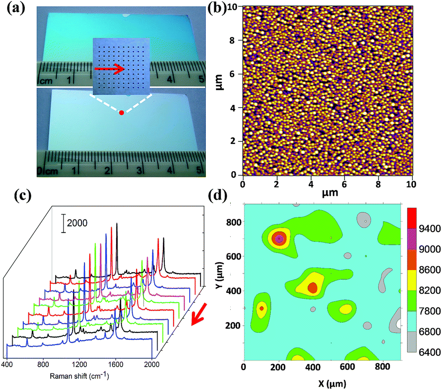 | ||
| Fig. 6 (a) Color change of the wafer-scale (2.5 × 5 cm cut) samples with the growth of Ag/a-Si nanosphere arrays and Ag/a-Si@Ag nanosphere arrays on Si substrates, respectively, inset shows an optical magnified view (×50 objective lens with NA = 0.5) of the red dot region with the point by point scanning mode (step-size of 100 μm). (b) AFM topography of a randomly selected area on the Ag/a-Si@Ag SERS substrate with a uniform distribution of NSs over a 10 μm × 10 μm area on the Si substrate. (c) Raman spectra from 10 different spots along the arrow as shown in inset of (a) with steps of 100 μm. (d) Planar Raman map of the intensities of Raman signals at 1076 cm−1 on the Ag/a-Si@Ag SERS substrate of the inset area marked in (a). | ||
Conclusions
For the first time, we demonstrated growth of Ag/a-Si@Ag nanosphere arrays on a Si substrate by a bottom-up method to work as a high-performance SERS substrate. With the help of the solid-state dewetting, high density Ag nanoparticle arrays were formed on Si substrate with large-area uniformity. By the adjustments of thicknesses of a-Si and Ag out-layer coating, the SERS properties can be optimized with the inter-particle spacing of the Ag/a-Si@Ag NSs limited to several nanometers. Based on the analysis of optical properties and SERS activities to p-Tc, we concluded that, the optimized SERS substrate performed with a high sensitivity with detection limit as low as 10−14 M and an enhancement factor up to 108. Furthermore, a wafer scale large-area uniformity and reproducibility of SERS signal were confirmed with small standard deviation, e.g., 8% at 1076 cm−1 and 9% at 1593 cm−1. The method present here can be extended to create a new class of highly sensitive SERS sensor with large-area output, and may play an important role in device design and the corresponding diverse chemical and biological detection.Acknowledgements
We acknowledge partial support by the financial support by the Natural Science Foundation of China (Grant no. 51202072), the State Key Program for Basic Researches of China (Grant no. 2015CB921202), the International Science & Technology Cooperation Platform Program of Guangzhou (Grant no. 2014J4500016), the Project for Guangdong Province Universities and Colleges Pearl River Scholar Funded Scheme (2014), the Program for Changjiang Scholars and Innovative Research Team in University (Grant no. IRTI1243), the European NODE project 015783 and by the DFG project GO 704/5-1. The authors would also like to acknowledge Mr Guohui Lin for preparation of SEM samples.Notes and references
- J. E. M. Matthew, J. Banholzer, L. Qin and C. A. Mirkin, Chem. Soc. Rev., 2008, 37, 885 RSC.
- Y. Fang, N.-H. Seong and D. D. Dlott, Science, 2008, 321, 388 CrossRef CAS PubMed.
- F. J. García-Vidal and J. B. Pendry, Phys. Rev. Lett., 1996, 77, 1163 CrossRef.
- T. Haibin, M. Guowen, H. Qing, Z. Zhuo, H. Zhulin and Z. Chuhong, Adv. Funct. Mater., 2012, 22, 1 CrossRef.
- J. A. Dieringer, R. B. Lettan, K. A. Scheidt and R. P. Van Duyne, J. Am. Chem. Soc., 2007, 129, 16249 CrossRef CAS PubMed.
- S. Nie and S. R. Emory, Science, 1997, 275, 1102 CrossRef CAS PubMed.
- Z. Liu, Z. Yang, B. Peng, C. Cao, C. Zhang, H. You, Q. Xiong, Z. Li and J. Fang, Adv. Mater., 2014, 26, 2431 CrossRef CAS PubMed.
- Y. Shikuan, C. Weiping, K. Lingce and L. Yong, Adv. Funct. Mater., 2010, 20, 2527 CrossRef.
- J. A. Huang, Y. Q. Zhao, X. J. Zhang, L. F. He, T. L. Wong, Y. S. Chui, W. J. Zhang and S. T. Lee, Nano Lett., 2013, 13, 5039 CrossRef CAS PubMed.
- C. Qian, C. Ni, W. Yu, W. Wu, H. Mao, Y. Wang and J. Xu, Small, 2011, 7, 1800 CrossRef.
- M. Khorasaninejad, J. Walia and S. S. Saini, Nanotechnology, 2012, 23, 275706 CrossRef CAS PubMed.
- R. Alvarez-Puebla, B. Cui, J. P. Bravo-Vasquez, T. Veres and H. Fenniri, J. Phys. Chem. C, 2007, 111, 6720 CAS.
- H. H. Wang, C. Y. Liu, S. B. Wu, N. W. Liu, C. Y. Peng, T. H. Chan, C. F. Hsu, J. K. Wang and Y. L. Wang, Adv. Mater., 2006, 18, 491 CrossRef CAS.
- S. Kim, L. Piao, D. Han, B. J. Kim and T. D. Chung, Adv. Mater., 2013, 25, 2056 CrossRef CAS PubMed.
- F. Cosmin and A. Simion, J. Phys. Chem. C, 2010, 114, 11717 Search PubMed.
- W. Chunxu, R. Weidong, J. Nan, J. Wei, L. Sa, Z. Chun and Z. Bing, J. Phys. Chem. C, 2010, 114, 2886 Search PubMed.
- M. C. Günendi, İ. Tanyeli, G. B. Akgüç, A. Bek, R. Turan and O. Gülseren, Opt. Express, 2013, 21, 18344 CrossRef PubMed.
- B. T. Alexander, C. Lev, K. Tanya, A. B. Tatyana, H. Gilad, V. Alexander and R. Israel, J. Phys. Chem. C, 2011, 115, 24642 Search PubMed.
- Z. Huang, N. Geyer, P. Werner, J. Boor and U. Gosele, Adv. Mater., 2011, 23, 285 CrossRef CAS PubMed.
- F. Ruffino and M. Grimaldi, Appl. Surf. Sci., 2013, 270, 697 CrossRef CAS PubMed.
- Z. S. Hu, Z. Liu, L. Li, B. G. Quan, Y. L. Li, J. J. Li and C. Z. Gu, Small, 2014, 10, 3932 CrossRef CAS.
- M. M. Jeffrey, L. Shuzhou, K. A. Logan and C. S. George, J. Phys. Chem. C, 2012, 116, 1627 Search PubMed.
- M. Chirumamilla, A. Toma, A. Gopalakrishnan, G. Das, R. P. Zaccaria, R. Krahne, E. Rondanina, M. Leoncini, C. Liberale, F. De Angelis and E. Di Fabrizio, Adv. Mater., 2014, 26, 2353 CrossRef CAS PubMed.
- C. M. Müller, F. C. Mornaghini and R. Spolenak, Nanotechnology, 2008, 19, 485306 CrossRef PubMed.
- M. Schade, O. Varlamova, J. Reif, H. Blumtritt, W. Erfurth and H. S. Leipner, Anal. Bioanal. Chem., 2010, 36, 1905 CrossRef PubMed.
- H. Dai, M. Li, Y. Li, H. Yu, F. Bai and X. Ren, Opt. Express, 2012, 20, 9 Search PubMed.
- J. Ye, F. Wen, H. Sobhani, J. B. Lassiter, P. V. Dorpe, P. Nordlander, N. J. Halas, P. Nordlander and N. Halas, Nano Lett., 2012, 12, 1660 CrossRef CAS PubMed.
- W. Li, P. H. Camargo, X. Lu and Y. Xia, Nano Lett., 2009, 9, 485 CrossRef CAS PubMed.
- G. Sauer, G. Brehm and S. Schneider, J. Raman Spectrosc., 2004, 35, 568 CrossRef CAS.
- O. Masatoshi, M. Naoki, Y. Katsumasa and U. Isamu, J. Phys. Chem., 1994, 98, 12702 CrossRef.
- M. Hentschel, D. Dregely, R. Vogelgesang, H. Giessen and N. Liu, ACS Nano, 2011, 5, 2042 CrossRef CAS PubMed.
- S. Kleinman, R. Frontiera, A. Henry, J. Dieringer and P. V. Duyne, Phys. Chem. Chem. Phys., 2013, 15, 21 RSC.
- E. Ru, M. Blackie, M. Meyer and E. Etchegoin, J. Phys. Chem. C, 2007, 111, 13794 Search PubMed.
- Z. Ming-Liang, F. Xia, Z. Hong-Wei, S. Ming-Wang, J. A. Zapien, W. Ning-Bew and L. Shuit-Tong, J. Phys. Chem. C, 2010, 114, 1969 Search PubMed.
- L. Hongyan, L. Zhipeng, W. Wenzhong, W. Youshi and X. Hongxing, Adv. Mater., 2009, 21, 4614 CrossRef.
- M. J. Natan, Faraday Discuss., 2006, 132, 321 RSC.
Footnote |
| † Electronic supplementary information (ESI) available: Fig. S1–S9, calculation of enhancement factor (EF). See DOI: 10.1039/c5ra00512d |
| This journal is © The Royal Society of Chemistry 2015 |