
 Open Access Article
 This Open Access Article is licensed under a
 Creative Commons Attribution 3.0 Unported Licence
Carbon nanotube diameter control via catalytic Co nanoparticles electrodeposited in porous alumina membranes†
N. J.
Ke
,
A. J.
Downard
* and
V. B.
Golovko
*
The MacDiarmid Institute for Advanced Materials and Nanotechnology, Department of Chemistry, University of Canterbury, Private bag 4800, Christchurch 8140, New Zealand. E-mail: alison.downard@canterbury.ac.nz; vladimir.golovko@canterbury.ac.nz
First published on 3rd March 2015
Abstract
Use of porous anodic alumina (PAA) membranes prevents sintering of metal catalyst particles during growth of carbon nanotubes (CNTs) by chemical vapour deposition (CVD). When a metal catalyst fills the base of the pores, the diameters of the resulting CNTs match those of the pores. This approach is generally limited to PAA membranes with pores ≥50 nm in diameter presumably due to difficulties associated with metal deposition in very narrow pores and with mass transport of gases during CVD. However, PAA membranes offer the opportunity to grow CNTs using catalyst particles with diameters that are significantly smaller than the pores. Here we investigate the electrodeposition of small amounts of Co into the pores of shallow PAA membranes. Using alternating voltage deposition with membranes that have intact, but thinned, barrier layers we demonstrate that CNTs with a diameter of 25 ± 3 nm can be grown from pores with diameters of 60 ± 4 nm.
Introduction
Porous anodic alumina (PAA) is a popular template for the fabrication of highly ordered nanostructures such as metal and semiconductor nanowires (NWs) and carbon nanotubes (CNTs).1 The widespread use of PAA templates relies on its ease of fabrication, low cost and high thermal stability, coupled with the wide range of pore sizes and aspect ratios that can be achieved through control of the anodisation conditions. For fabrication of NWs, metal or semiconductor is deposited in the membrane pores and the resulting structures have diameters matching those of the pores.2–9 Growth of CNTs by chemical vapour deposition (CVD) can occur through two mechanisms in PAA membranes: multi-walled (MW) CNTs can be grown from transition metal nanoparticles (NPs) and NWs deposited within the pores, whereas disordered CNTs can grow by pyrolysis of the carbon feedstock gas on the pore walls themselves.10 When the carbon source for CVD is CO, or when H2 is added to the commonly used C2H2, catalysis by transition metal particles is the dominant CNT growth mechanism in PAA templates.10A major advantage of growing CNTs from catalyst particles within PAA membrane pores is that particle aggregation cannot occur at the elevated temperatures required for CNT growth. This results in a maximum CNT diameter defined by the diameter of the pores; indeed, in most reports to date, the CNT diameters match those of the pores, presumably because the metal catalyst completely fills the bottom of the pores.10–17 A survey of the literature indicates that growth of CNTs is typically undertaken in PAA membranes with pores ≥50 nm in diameter. Growing lower diameter CNTs by this strategy is problematic because as the pore diameter decreases, deposition of metal catalyst into the base of the pores and mass transport of gases into the pores during CVD is hindered. To grow sub-50 nm diameter CNTs while avoiding the challenges of working with low diameter pores, Suh and co-workers developed the strategy of depositing metal into narrow pores and then widening the pores by etching the membrane.18,19 In one example, Co was electrodeposited near the mouth of the pores (diameter ∼ 29 nm) of a PAA membrane which was then etched to widen the pores to ∼65 nm. CNTs with a uniform diameter of 32 nm were grown from the template.19 In later work, Fe(III) solution was deposited on top of the electrodeposited Co and after pore widening, CVD growth yielded CNTs with diameters ranging from 7 to 17 nm, depending on the concentration of Fe(III) solution.18 In a refinement of the latter method, Fe(III) solution was introduced into the pores (diameter ∼ 50 nm) of a PAA membrane bonded to a Si wafer. To ensure that a uniform amount of Fe(III) was deposited in each pore, the membrane was dried on a magnet. CNTs with diameters down to 5 nm were grown from these templates; the CNT diameters were shown to correspond to the size of the Fe nanoparticles generated in the PAA membrane.20
Three general methods have been utilised for the electrodeposition of metals and semiconductors into the pores of PAA membranes. Firstly, free-standing, membranes with through-holes at the base of the pores can be prepared by complete removal of the Al substrate and the oxide barrier layer at the pore base followed by deposition of an inert metal layer (sputtered or evaporated) onto one side which can then act as the working electrode for electrodeposition.4,9,16,21–23 Alternatively, an Al layer can be sputtered onto a conducting substrate and after anodisation, the barrier layer can be completely removed to expose the underlying conducting surface which becomes the working electrode.7,14,24,25 In the third approach, the Al substrate is left intact after anodisation but the insulating barrier layer is substantially thinned. Pulsed current or pulsed voltage electrodeposition is performed directly on the membrane and NPs or NWs are deposited in the pores where the oxide layer is the least insulating.17,26–30
In the present work we aim to fabricate CNTs in PAA templates such that the CNT diameters are lower than the diameters of the pores. We have used the technically simplest method to electrodeposit small amounts of Co directly into the pores of PAA membranes under conditions that are expected to result in formation of NPs that do not completely fill the base of the pores. We employ pulsed voltage electrodeposition of Co directly into the pores after thinning of the oxide barrier layer. In order to ensure unhindered mass transport of gases during CVD, we have fabricated shallow PAA membranes; shallow membranes were also expected to assist with reproducible electrodeposition of Co by maximising mass transport of Co(II) to the base of the pores.
Experimental
High-purity aluminium foil (99.9995%, Puratronic) with thickness 0.5 mm was degreased by sonication in acetone for 30 min. All samples underwent a first anodisation at 30 V in 0.4 M oxalic acid at 16 ± 1 °C for 2 h. After removal of the alumina layer in a solution of 0.4 M H3PO4 and 0.1 M H2CrO4 at 70 ± 1 °C for 40–60 min, a second anodisation was performed for a selected time as specified in the Results and discussion section. At the end of the second anodisation, the barrier layer was thinned and pore branching was induced in the base of the pores by dropping the voltage from 30 to 10 V at a rate of 1 V min−1 followed by 3 min at 10 V to allow equilibration of the barrier layer.29,31 For some experiments, the alumina film was removed after the second anodisation and a brief third anodisation was carried out, using the same conditions as above, but with an anodisation time of 10–30 s. At the end of the anodisation, the voltage was dropped as described above. After the final anodisation, the sample was chemically etched by immersion in 0.1 M H3PO4 at 30 °C. The optimised protocol involved anodisations for 2 h, 1 h and 30 s, with removal of the alumina layer after the first and second anodisations and chemical etching for 65 min after the third anodisation.32 PAA membranes were stored in Millipore Milli-Q water (resistivity > 18 MΩ cm) until use in electrodeposition experiments.Co was electrodeposited in the membrane pores from a solution of 0.85 M CoSO4 and 0.64 M H3BO3 (pH 3.8) or after adjusting the pH to 4.7 with 0.1 M NaOH. The solution was purged with N2 for 15 min prior to electrodeposition and a N2 atmosphere was maintained throughout the procedure. A sequence of 10 ms pulses with amplitude ±10 V was applied, starting at −10 V and finishing at +10 V. These pulses were applied for different amounts of time (see text) and in some experiments, the pulse sequences were periodically interrupted with a 15 min rest period at open circuit potential. After deposition of Co, AAO templates were rinsed with N2-purged Milli-Q water and dried with a stream of N2.
For CNT growth by chemical vapour deposition (CVD), the standard protocol entailed heating the template to 650 °C in a tube furnace under an Ar flow (90 sccm). While maintaining the temperature at 650 °C, H2 (30 sccm), was introduced for 60 min to promote reduction of Co oxides followed by growth of CNTs for 23 min in an atmosphere of Ar (90 sccm), H2 (20 sccm) and C2H2 (20 sccm). The samples were cooled under Ar flow (200 sccm).
Field emission scanning electron microscopy (FESEM) images were obtained using a Jeol JSM 7000 FESEM, operating with an accelerating voltage ranging from 5 kV to 15 kV and with working distance ranging from 5 to 15 mm. The dimensions of PAA pores and CNTs were determined from SEM images using Image J software. Atomic force microscopy (AFM) images were obtained with a Digital Instruments Dimension 3100 microscope. Raman spectra were recorded in the backscattering mode using a 633 nm He–Ne laser focused on the sample by means of a 100× objective of 1 numerical aperture. The CCD detector was coupled to a high resolution monochromator (Jovin Yvon, T-64000).
Results and discussion
Preparation of PAA membranes
Experiments aimed at optimising the conditions for preparation of PAA membranes were guided by the assumption that uniform deposition of catalytic Co NPs in the base of the pores of PAA membranes would be promoted by use of ‘soft’ alumina membranes with highly uniform pore structures and barrier layers amenable to electrochemical and chemical thinning. Restricting the pore depth to ≤500 nm was expected to have the further advantage of facilitating mass transport of Co(II) ions to the base of the pores during electrodeposition, and mass transport of gases to the catalyst particles during CNT growth by CVD.All anodisations were carried out under mild conditions (30 V in 0.4 M oxalic acid at 16 ± 1 °C). A relatively long first anodisation time of 2 h was used to allow self-ordering of the porous structure which would give, after removal of the alumina layer, an ordered dimpled template for the second anodisation step. To obtain the desired shallow membrane, a very brief second anodisation was attempted. Fig. 1a shows that when the second anodisation was 90 s, a membrane with a wide range of pore sizes and shapes was obtained. The sample was bent to crack the PAA membrane and then imaged by SEM (Fig. 1b), revealing a pore depth of approximately 500 nm (note that there is considerable uncertainty in this value because the tilt angle of the sample in the image is unknown). Clearly the 90 s second anodisation gives the desired shallow membrane but not a well-ordered porous structure.
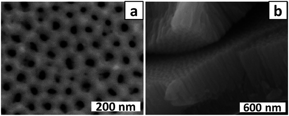 | ||
| Fig. 1 (a) Top view and (b) cross-section view SEM images of a PAA membrane fabricated using a two-step anodisation with second anodisation time = 90 s. | ||
Preparation of a well-ordered membrane using a very brief anodisation relies on the starting template (for the final anodisation) being well-ordered because pore self-ordering during a brief anodisation will be limited.33 AFM imaging (Fig. 2a and c) confirmed that the dimpled substrate prepared by a 2 h anodisation followed by dissolution of the alumina layer was poorly ordered. The measured depth of dimples ranges from 13 to 26 nm; deeper dimples may be present but are not adequately imaged by AFM due to their higher aspect ratio.
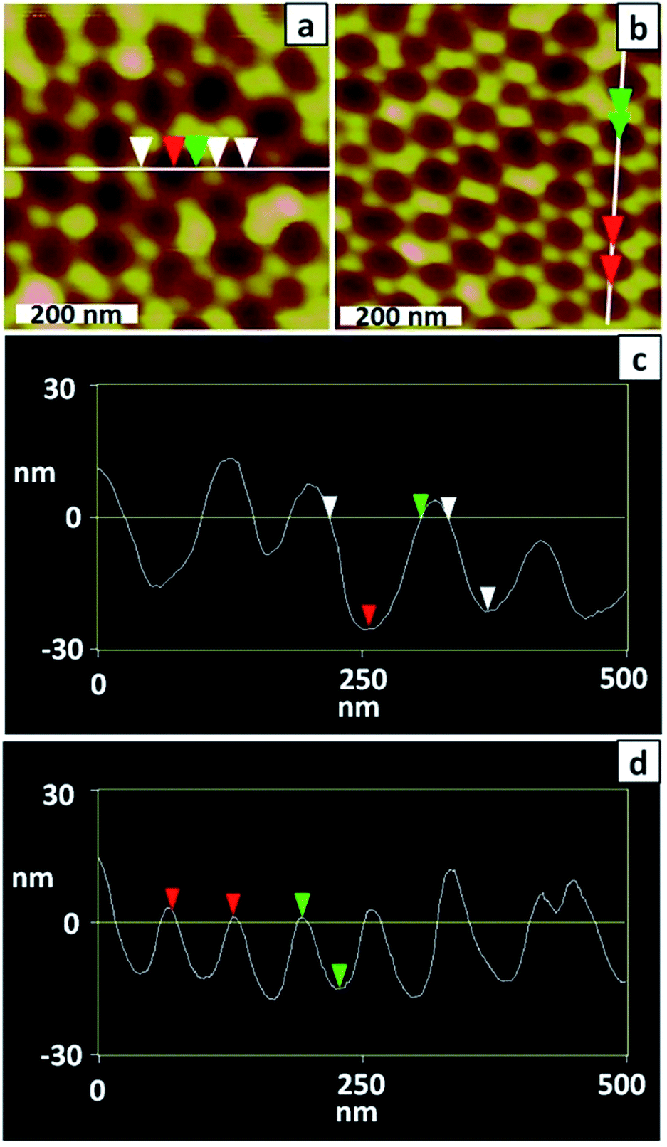 | ||
| Fig. 2 (a and b) AFM topographical images and (c and d) line profiles of a PAA membrane after the (a and c) first anodisation and (b and d) second anodisation (1 h). | ||
To improve the uniformity of the shallow PAA membrane, an additional anodisation step was introduced. Several reports describe use of multiple anodisation steps, with removal of alumina between each step, as a means of improving the uniformity of the porous structure.34,35 Following this strategy a three-step anodisation protocol was optimised. Two relatively long anodisations were used to improve the uniformity of the dimpled template, whereas the third anodisation was very brief to ensure formation of a shallow membrane. The standard procedure involved a first anodisation for 2 h, a second for 1 h and a third for 30 s, with removal of the alumina after the first and second anodisations. The AFM images of Fig. 2b and d confirm that the longer second anodisation improves the uniformity of the dimpled template. The measured dimple depth ranges between 13 and 17 nm and the dimple arrangement is more ordered than after the first anodisation. Fig. 3a and b show SEM images of a typical PAA membrane prepared using the standard three-step protocol, and a histogram (Fig. 3c) of pore diameters obtained from the SEM image in Fig. 3a. The average pore diameter is 28 ± 5 nm and the pore depth is approximately 300 nm (Fig. 3b). Use of a shorter (10 s) third anodisation gave a membrane with a wide range of pore sizes and hence 30 s was adopted as the standard third anodisation time.
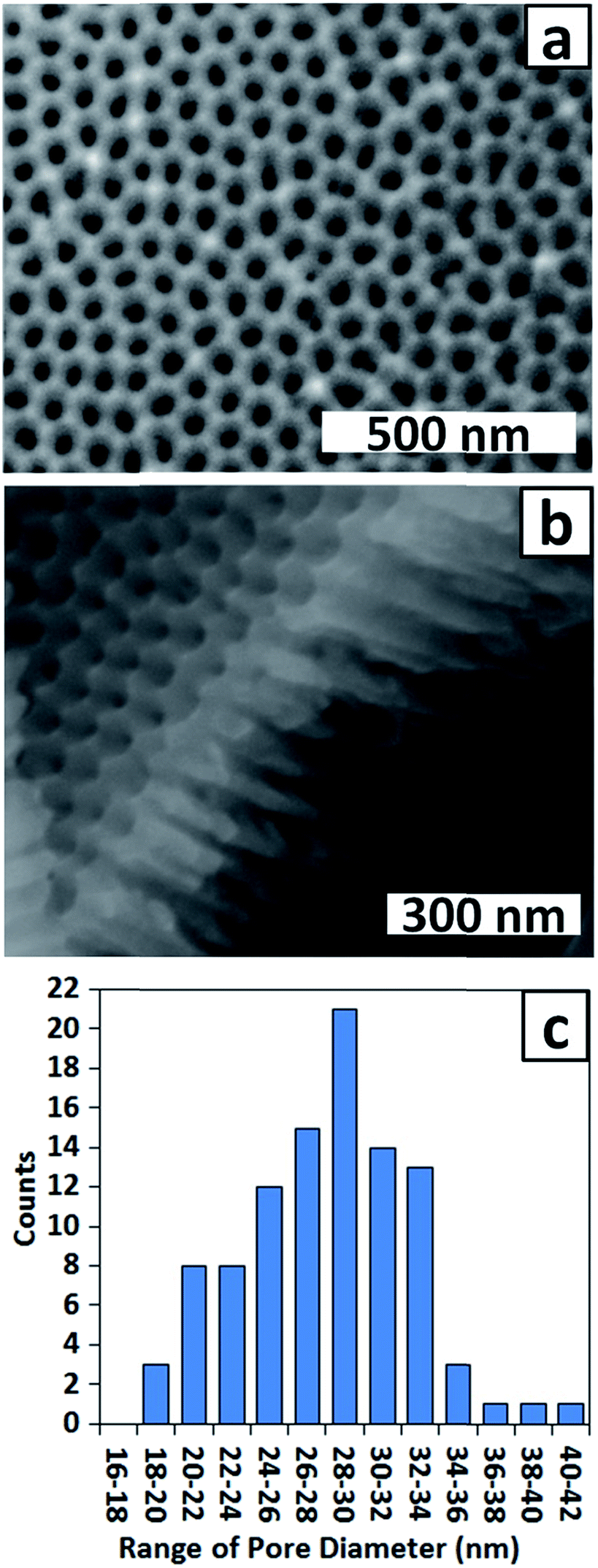 | ||
| Fig. 3 (a) Top view and (b) side view SEM images of a PAA membrane and (c) corresponding histogram of pore diameters after a three-step anodisation. Third anodisation time = 30 s. | ||
For use of the membrane as a template for electrodeposition of Co NPs, minimising the thickness of the alumina barrier layer at the base of the pores (in addition to pore end branching induced by dropping the voltage36) is important for maximising its conductivity. During barrier layer thinning by chemical etching, the pore walls are also thinned (although at a lower rate37) which for the present work has the advantage of improving mass transport of solution species and gases into the pores. The effect of immersion of PAA membranes in 0.1 M H3PO4 at 30 ± 1 °C 32 for 60, 65 and 75 min is shown in the top-view SEM images and the corresponding histograms of pore diameters in Fig. 4. Etching for 60 min (Fig. 4a and b) increased the pore diameter from 28 ± 5 (Fig. 3) to 48 ± 4 nm and the distribution of pore diameters has narrowed. Etching for 65 min (Fig. 4c and d) further increased the average pore diameter to 60 ± 4 nm while after 75 min (Fig. 4e and f) the average pore diameter was greater still but there was also a greater distribution of pore diameters (63 ± 6 nm) and some walls have been dissolved completely, which is highly undesirable as catalyst particle aggregation can now occur. Based on the requirement for a uniform porous structure with maximum pore diameter and (presumably) minimum barrier layer thickness without breaking pore walls, 65 min was chosen as the standard chemical etching time.
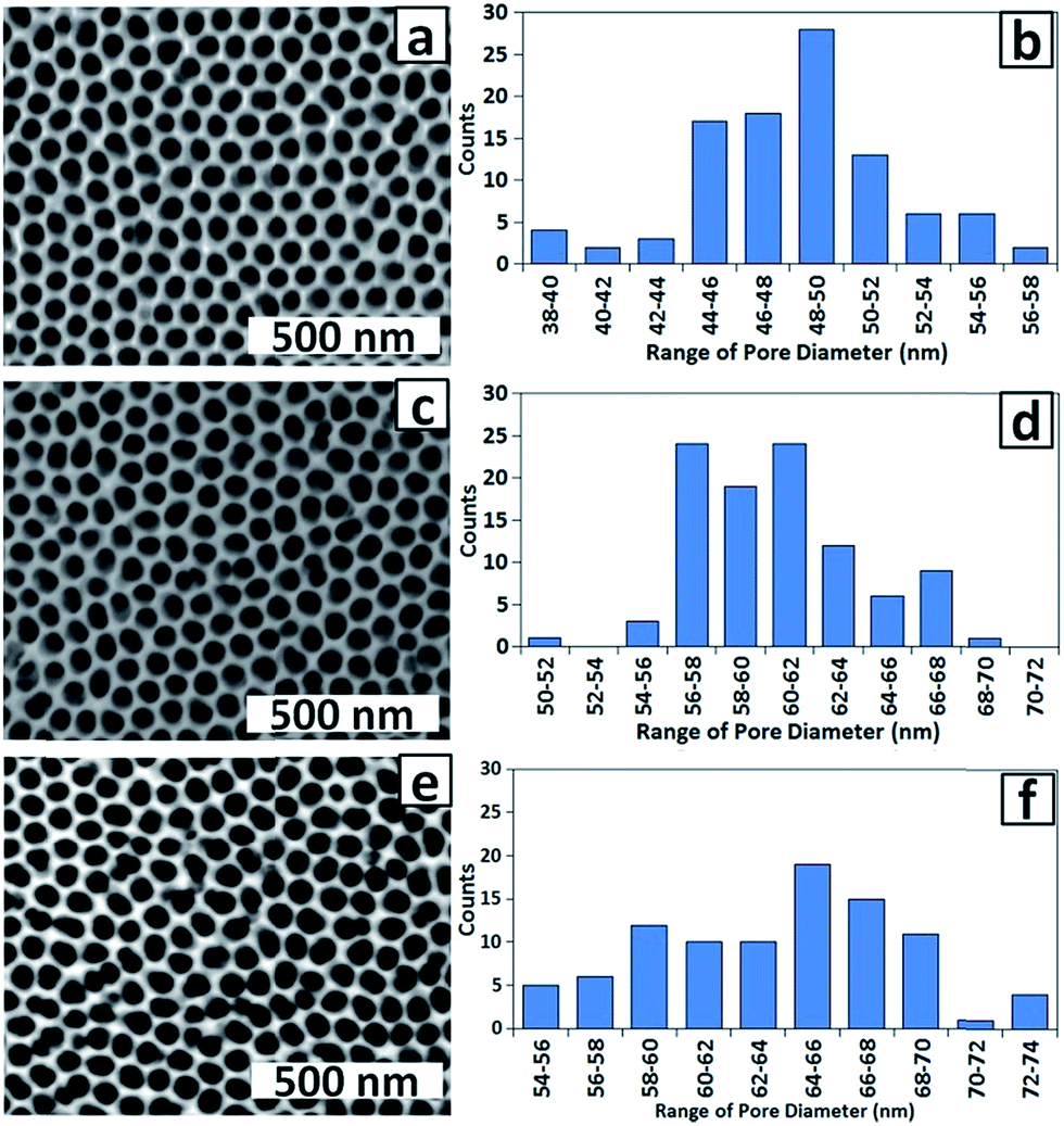 | ||
| Fig. 4 SEM images and corresponding histograms of pore diameters for PAA membranes chemically etched for (a and b) 60 min; (c and d) 65 min and (e and f) 70 min. | ||
Growth of CNTs by CVD
Our goal is to control the diameters of catalytically grown CNTs by controlling the size and reactivity of Co NP catalysts electrodeposited in the pores of PAA membranes. However direct comparison of the sizes of electrodeposited Co NPs and the CNTs subsequently grown on a template was not experimentally feasible in this study. (‘Template’ denotes a PAA membrane with deposited Co NPs.) Although SEM or TEM imaging of NPs (larger than those in the present work) within PAA templates has been reported in a limited number of studies,10,29,38 these techniques have the disadvantage of requiring the template to be cut or partially removed prior to imaging. Methods such as chemical etching or mechanical bending may result in loss of the electrodeposited metal NPs from the template. Furthermore, destruction of the template effectively doubles the required number of samples per study, because separate samples are required for imaging of NPs and of CNT growth. These factors would make it difficult to obtain statistically significant datasets of NP and CNT size. An additional difficulty of direct SEM imaging for the present study is the small size of the electrodeposited NPs and the low contrast between the NPs and PAA template. Fig. S1, ESI,† shows an image of the cross-section of a bent template and illustrates these difficulties.Consideration of the issues described above led us to use an indirect method to assess our progress towards electrodeposition of uniform arrays of Co NPs. We examined the CNTs grown by a standard CVD procedure using PAA templates prepared under different conditions and assumed that CNT diameters matched those of the NPs. This approach is based on a number of earlier reports which demonstrate correlations between the size of catalytic NPs and CNT diameters.18,39–42 Use of this indirect method for monitoring the preparation of catalytically active Co NP arrays was experimentally convenient but relies on an optimised protocol for CNT growth. In preliminary experiments we established that the key to reproducible CNT growth was use of a sufficiently high temperature for reduction of the Co NP catalyst which is readily oxidised during handling in air. The temperature required for complete reduction of Co oxides has been shown to depend on the heating rate, particle size and the support material43,44 but is typically ≥600 °C under a flow of H2 and an inert gas. For the PAA templates supported on Al used in this work, 650 °C was selected as the maximum that could be used without melting the Al underlayer. Our protocol was based on that of Jeong et al.10 who also used a growth temperature of 650 °C.
Prior to systematic investigation of the electrodeposition of Co NPs, the growth of CNTs on PAA templates by the optimised CVD method was confirmed by Raman spectroscopy. Samples gave the expected G, D and G′ bands (Fig. 5) consistent with the growth of MWCNTs.45
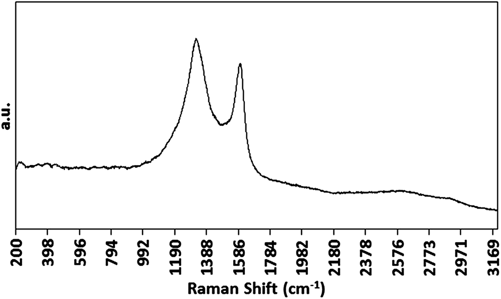 | ||
| Fig. 5 Raman spectrum of CNTs grown on a PAA template prepared using a Co electrodeposition time of 100 ms. | ||
Electrodeposition of Co NPs in shallow PAA membranes
An alternating deposition voltage has been widely used for the electrodeposition of NPs and nanowires within PAA membranes with intact barrier layers.29,46–49 The method relies on the rectifying property of the barrier layer which allows cathodic but not anodic current to flow. As a consequence, metal ions are reduced during the negative voltage pulse but the deposited metal is not electrooxidised during the positive pulse. The conditions used in this work, namely a square waveform with amplitude ±10 V, frequency 100 Hz and reductive/anodic pulse polarity, were selected by consideration of those reported for electrodeposition of metal nanostructures into similar membranes.29 Pulsed electrodeposition was also investigated in which 100 ms periods of alternating voltage deposition at 100 Hz were separated by a 15 min rest period at open circuit voltage. The purpose of the rest period was to ensure replenishment of ions in the pores and to allow diffusion of H2 from the pores. Using the strategy of CVD growth of CNTs from PAA templates as a means to evaluate the size and uniformity of Co NP deposition, the influence of several factors on electrodeposition was systematically investigated.After electrodeposition of Co, the template was rinsed in water. The rinsing step was implemented to ensure that any residual Co(II) ions present on or in the membrane would be removed and only Co electrodeposited in the pores would remain, thus allowing control over the total amount of Co in the template. In the standard protocol, electrodeposition was performed in the absence of O2. In preliminary experiments, it became apparent that excluding O2 during rinsing of the prepared template was also important. When O2 was not excluded, subsequent CNT growth was very sparse and irreproducible suggesting that a significant proportion of Co NPs were oxidised and dissolved during washing. To avoid this problem, in all further experiments, templates were rinsed in N2 saturated water and dried under a stream of N2.
The effect of pH of the Co(II) electrolyte solution during electrodeposition was investigated by examining CNT growth on the PAA templates. Fig. 6a and c show top view SEM images of CNTs grown from PAA templates prepared by electrodeposition of Co NPs from pH 3.8 and 4.7 solutions, respectively. Although the CNTs diameters for both samples (average ∼ 32 nm) are significantly smaller than the pore diameter (∼60 nm), the corresponding histograms of CNT diameters (Fig. 6b and d) indicate that a much narrower distribution is obtained after electrodeposition of Co NPs at pH 4.7 than at pH 3.8. This indicates that deposition of Co NPs is more uniform at the higher pH consistent with the expected decreased rate of H+ reduction and H2 bubble formation. Reduction of protons competes with reduction of metal ions during electrodeposition and the generated H2 bubbles can block the pores, preventing metal deposition.27 A solution pH of 4.7 was therefore adopted as the standard for electrodeposition.
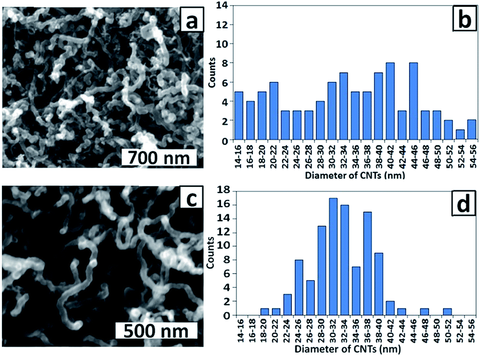 | ||
| Fig. 6 SEM images and corresponding histograms of CNT diameters for CNTs grown on PAA templates prepared with Co electrodeposition (4 × 100 ms) at (a and b) pH 3.8 and (c and d) pH 4.7. | ||
The effect of Co electrodeposition time on the diameter of CNTs grown by CVD from PAA templates, and by inference, the size of Co NPs deposited in the PAA membrane, was examined in a series of experiments. The alternating deposition voltage was applied for 20, 8 and 4 × 100 ms periods, separated by rest periods of 15 min. Single 100 and 50 ms depositions were also included. Fig. 7 shows SEM top view images of the templates after CNT growth and the corresponding histograms of CNT diameters.
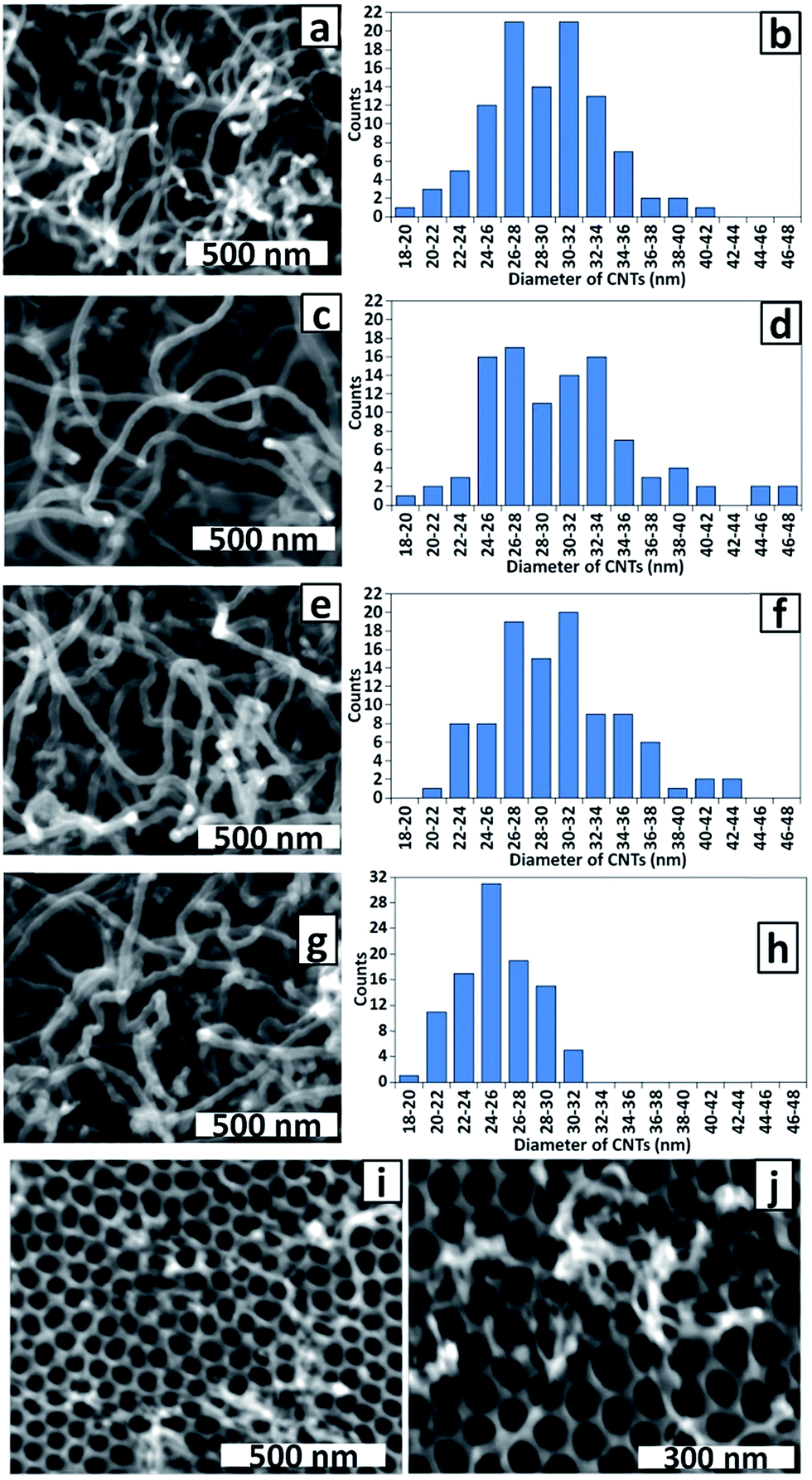 | ||
| Fig. 7 SEM images and corresponding histograms of CNT diameters for CNTs grown on PAA templates prepared with Co electrodeposition times of (a and b) 20 × 100 ms; (c and d) 8 × 100 ms; (e and f) 4 × 100 ms and (g and h) 100 ms. (i) SEM image of CNTs grown on PAA template prepared with Co electrodeposition time 50 ms; (j) higher resolution image of sample shown in (i). | ||
As described above, a striking feature of all samples is the small CNT diameter compared with the pore diameter on the top surface of the membrane. Careful examination of high magnification SEM images of PAA membrane cross-sections in samples bent to enable imaging revealed that the pore diameters at the top and the bottom of the membrane are uniform (for an example see Fig. S1, ESI†). Hence the CNT diameter does not correspond to the pore diameter at the base of the membrane. We conclude that the electrodeposited Co NPs are smaller than the pores (that is, the pores are not being filled with ‘plugs’ of Co) and sub-pore diameter CNTs are achieved via control of the amount of the catalytically active metal, not the pore size.
Interestingly, the templates prepared with 20, 8 and 4 × 100 ms deposition periods yielded CNTs with very similar diameters, even though it was expected that the amount of deposited metal would increase with total deposition time. Monitoring the actual polarisation voltages at the electrodes during deposition revealed that the maximum negative and positive voltages decrease (become closer to zero) throughout each 100 ms deposition period indicating a decrease in conductivity (see ESI, Fig. S2 and S3†). The polarisation voltage is not restored to the initial value during the 15 min rest interval and continues to decrease during further deposition periods. Hence, based on the similarity of CNT diameters in these series it can be inferred that by the fourth deposition period, the polarisation voltage has dropped below that required for efficient reduction of Co(II).
Fig. 7g and h show that the diameters of CNTs grown from the template prepared with a single 100 ms deposition are smaller and have a narrower size distribution (25 ± 3 nm) than those grown after longer deposition times (Fig. 7a–f, average diameter 29–30 nm). This is fully consistent with the deposition of smaller Co NPs at the shorter deposition time and consequently the growth of CNTs that reflect the size difference. It is noteworthy that the size distributions shown in Fig. 6d (32 ± 6 nm) and Fig. 7f (30 ± 5 nm) are closely-matched as is expected for two samples prepared under the same conditions, confirming the reproducibility of our methods. Further evidence of CNT diameter control was gained using the template prepared with a single 50 ms deposition period. Fig. 7i and j shows there was only very sparse growth of CNTs with diameters too narrow to measure accurately by SEM. It is possible that traces of O2 readily dissolve the small Co NPs deposited under these conditions, accounting for the sparse CNT growth. Nevertheless, the growth of some smaller diameter CNTs is consistent with CNT morphology reflecting the Co NP size.
In a final set of experiments, the use of a dimpled substrate for Co NP electrodeposition was explored. The dimpled substrate was prepared by the standard first and second anodisations but the voltage was not dropped at the end of the second anodisation. Alumina was completely removed from the substrate leaving just the dimpled Al base; a thin alumina layer is expected to naturally re-form over the base on exposure to air. As described above, this procedure gives a dimple depth of 13–17 nm. The dimples are essentially extremely shallow pores which may have potential advantages over standard PAA membranes: in comparison to a standard PAA membrane, preparation of a dimpled substrate is experimentally simpler, mass transport limitations (during electrodeposition of metal catalysts and growth of CNTs) will be absent and removal of CNTs from the template is easier. Hence, it was of interest to explore whether Co NPs could be selectively deposited in the base of the dimples and whether the dimples can provide an adequate barrier to NP aggregation during the high temperature reduction and CVD processes.
Using the alternating voltage procedure described above, Co was electrodeposited on this substrate using deposition times of 10, 20, 50 and 100 ms. SEM examination (not shown) of the sample prepared with 50 ms electrodeposition revealed a sparse coverage of thin (∼10 nm diameter) Co NWs on the raised areas between the dimples as well as in the dimples. Deposition over the whole surface is attributed to the native oxide coating which is expected to be of similar thickness and hence conductivity over the whole surface. CNTs were grown by CVD on the dimpled templates; regardless of Co deposition time, all samples had a very wide range of CNT diameters (Fig. 8). However, there was a decrease in average CNT diameter and decrease in CNT density as the deposition time decreased, consistent with a decrease in the total amount of Co deposited. Although arrays of uniformly-sized Au nanoparticles have been fabricated on dimpled Ta templates by thermal dewetting of thin Au films,50,51 the non-uniform CNT growth observed in this work indicates that sintering of Co NPs and NWs during the reduction step that precedes CNT growth does not lead to uniform Co NP sizes.
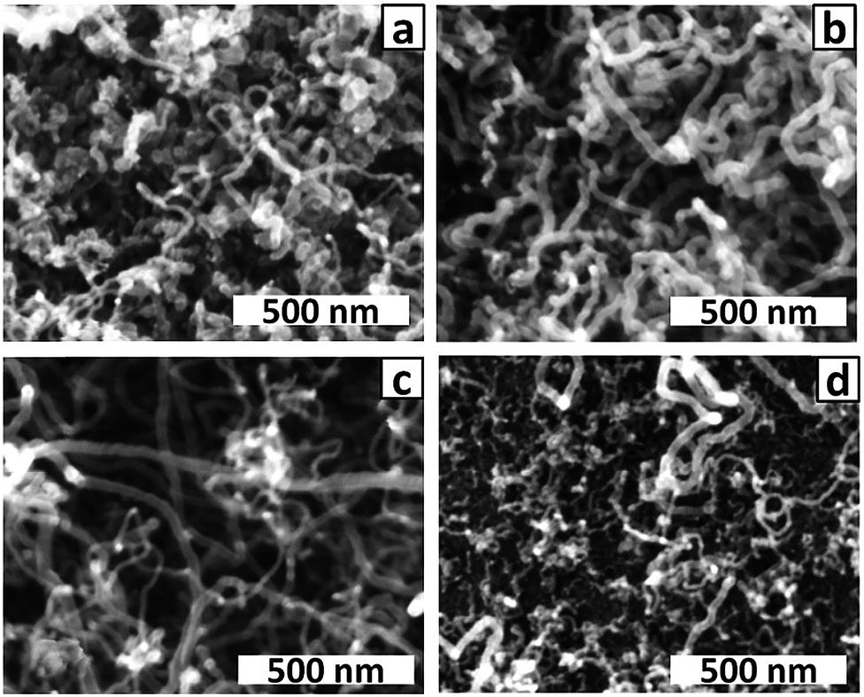 | ||
| Fig. 8 SEM images of CNTs grown on dimpled PAA templates prepared with Co electrodeposition times of (a) 100 ms; (b) 50 ms; (c) 20 ms and (d) 10 ms. | ||
Conclusions
We have demonstrated that control of CNT diameter is possible by depositing Co NPs in the pores of shallow PAA membranes under conditions where the diameters of the NPs are significantly smaller than the pore diameters of the PAA membrane. Alternating voltage deposition for 100 ms gave the most uniform size and coverage of CNTs while decreasing the deposition time decreased the uniformity of CNT coverage. Further optimisation of electrodeposition conditions is required to enable uniform deposition of Co NPs of any desired size. We found no evidence of sintering of Co NPs deposited in ∼300 nm deep pores, however, non-uniform sintering occurred on a dimpled substrate with dimple depth of 13–17 nm.Acknowledgements
The authors thank the MacDiarmid Institute for Advanced Materials and nanotechnology and the University of Canterbury for funding. The authors thank Eric Le Ru, Victoria University of Wellington, for Raman measurements and Rui Xu for his contribution to the early stages of this project.References
- C. T. Sousa, D. C. Leitao, M. P. Proenca, J. Ventura, A. M. Pereira and J. P. Araujo, Appl. Phys. Rev., 2014, 1, 031102 Search PubMed.
- H. Masuda and M. Satoh, Jpn. J. Appl. Phys., 1996, 35, L126 CAS.
- M. S. Sander, A. L. Prieto, R. Gronsky, T. Sands and A. M. Stacy, Adv. Mater., 2002, 14, 665–667 CrossRef CAS.
- A. Mao, N. G. Park, G. Y. Han and J. H. Park, Nanotechnology, 2011, 22, 175703 CrossRef PubMed.
- R. Li, Q. Chen, X. Hu, M. Wang, C. Wang and H. Zhong, RSC Adv., 2012, 2, 2250–2253 RSC.
- J. Y. Kim, S.-H. Lee, Y. Yan, J. Oh and K. Zhu, RSC Adv., 2012, 2, 8281–8285 RSC.
- D. K. Ivanou, Y. A. Ivanova, A. D. Lisenkov, M. L. Zheludkevich and E. A. Streltsov, Electrochim. Acta, 2012, 77, 65–70 CrossRef CAS PubMed.
- M. I. Irshad, F. Ahmad, N. M. Mohamed and M. Z. Abdullah, Int. J. Electrochem. Sci., 2014, 9, 2548–2555 CAS.
- H. R. Lim, S. Kim, Y. I. Lee, K. J. Lee and Y. H. Choa, J. Electrochem. Soc., 2014, 161, D442–D446 CrossRef CAS PubMed.
- S.-H. Jeong, H.-Y. Hwang, S.-K. Hwang and K.-H. Lee, Carbon, 2004, 42, 2073–2080 CrossRef CAS PubMed.
- J. Li, C. Papadopoulos, J. M. Xu and M. Moskovits, Appl. Phys. Lett., 1999, 75, 367–369 CrossRef CAS PubMed.
- J. S. Suh and J. S. Lee, Appl. Phys. Lett., 1999, 75, 2047–2049 CrossRef CAS PubMed.
- J. S. Lee, G. H. Gu, H. Kim, J. S. Suh, I. Han, N. S. Lee, J. M. Kim and G.-S. Park, Synth. Met., 2001, 124, 307–310 CrossRef CAS.
- S. H. Jeong and K. H. Lee, Synth. Met., 2003, 139, 385–390 CrossRef CAS.
- T. Yanagishita, M. Sasaki, K. Nishio and H. Masuda, Adv. Mater., 2004, 16, 429–432 CrossRef CAS.
- G. Meng, Y. J. Jung, A. Cao, R. Vajtai and P. M. Ajayan, Proc. Natl. Acad. Sci. U. S. A., 2005, 102, 7074–7078 CrossRef CAS PubMed.
- G. P. Sklar, K. Paramguru, M. Misra and J. C. LaCombe, Nanotechnology, 2005, 16, 1265–1271 CrossRef CAS.
- L. Kim, E.-M. Lee, S.-J. Cho and J. S. Suh, Carbon, 2005, 43, 1453–1459 CrossRef CAS PubMed.
- J. S. Lee and J. S. Suh, J. Appl. Phys., 2002, 92, 7519 CrossRef CAS PubMed.
- H. Y. Jung, S. M. Jung, L. Kim and J. S. Suh, Carbon, 2008, 46, 969–973 CrossRef CAS PubMed.
- M. S. Sander, R. Gronsky, T. Sands and A. M. Stacy, Chem. Mater., 2003, 15, 335–339 CrossRef CAS.
- F. S. Ou, M. M. Shaijumon, L. Ci and P. M. Ajayan, Carbon, 2007, 45, 1713–1716 CrossRef CAS PubMed.
- J. Fu, S. Cherevko and C. H. Chung, Electrochem. Commun., 2008, 10, 514–518 CrossRef CAS PubMed.
- T. Iwasaki, T. Motoi and T. Den, Appl. Phys. Lett., 1999, 75, 2044–2046 CrossRef CAS PubMed.
- O. J. Lee, S. K. Hwang, S. H. Jeong, P. S. Lee and K. H. Lee, Synth. Met., 2005, 148, 263–266 CrossRef CAS PubMed.
- K. Wada, T. Hatano and K. Uchida, J. Appl. Electrochem., 1979, 9, 445–455 CrossRef CAS.
- K. Nielsch, F. Muller, A. P. Li and U. Gosele, Adv. Mater., 2000, 12, 582–586 CrossRef CAS.
- S.-H. Jeong, H.-Y. Hwang, K.-H. Lee and Y. Jeong, Appl. Phys. Lett., 2001, 78, 2052–2054 CrossRef CAS PubMed.
- N. J. Gerein and J. A. Haber, J. Phys. Chem. B, 2005, 109, 17372–17385 CrossRef CAS PubMed.
- C. T. Sousa, D. C. Leitao, M. P. Proenca, A. Apolinario, J. G. Correia, J. Ventura and J. P. Araujo, Nanotechnology, 2011, 22, 315602 CrossRef CAS PubMed.
- G. Sharma, M. V. Pishko and C. A. Grimes, J. Mater. Sci., 2007, 42, 4738–4744 CrossRef CAS.
- J. Li, M. Moskovits and T. L. Haslett, Chem. Mater., 1998, 10, 1963–1967 CrossRef CAS.
- J. H. Yuan, F. Y. He, D. C. Sun and X. H. Xia, Chem. Mater., 2004, 16, 1841–1844 CrossRef CAS.
- C. K. Chen and S. H. Chen, Nanoscale Res. Lett., 2012, 7, 122 CrossRef PubMed.
- S. K. Hwang, J. Lee, S. H. Jeong, P. S. Lee and K. H. Lee, Nanotechnology, 2005, 16, 850–858 CrossRef CAS.
- W. L. Cheng, M. Steinhart, U. Gosele and R. B. Wehrspohn, J. Mater. Chem., 2007, 17, 3493–3495 RSC.
- C. Y. Han, G. A. Willing, Z. L. Xiao and H. H. Wang, Langmuir, 2007, 23, 1564–1568 CrossRef CAS PubMed.
- M. Sun, G. Zangari, M. Shamsuzzoha and R. M. Metzger, Appl. Phys. Lett., 2001, 78, 2964–2966 CrossRef CAS PubMed.
- S. N. Zaretskiy, Y.-K. Hong, D. H. Ha, J.-H. Yoon, J. Cheon and J.-Y. Koo, Chem. Phys. Lett., 2003, 372, 300–305 CrossRef CAS.
- X. Liu, T. P. Bigioni, Y. Xu, A. M. Cassell and B. A. Cruden, J. Phys. Chem. B, 2006, 110, 20102–20106 CrossRef CAS PubMed.
- O. A. Nerushev, S. Dittmar, R.-E. Morjan, F. Rohmund and E. E. B. Campbell, J. Appl. Phys., 2003, 93, 4185–4190 CrossRef CAS PubMed.
- D. O. Shin, D. H. Lee, H.-S. Moon, S.-J. Jeong, J. Y. Kim, J. H. Mun, H. Cho, S. Park and S. O. Kim, Adv. Funct. Mater., 2011, 21, 250–254 CrossRef CAS.
- H.-Y. Lin and Y.-W. Chen, Mater. Chem. Phys., 2004, 85, 171–175 CrossRef CAS PubMed.
- B. H. Liu, J. Ding, Z. Y. Zhong, Z. L. Dong, T. White and J. Y. Lin, Chem. Phys. Lett., 2002, 358, 96–102 CrossRef CAS.
- P. C. Eklund, J. M. Holden and R. A. Jishi, Carbon, 1995, 33, 959–972 CrossRef CAS.
- D. Al Mawlawi, N. Coombs and M. Moskovits, J. Appl. Phys., 1991, 70, 4421–4425 CrossRef CAS PubMed.
- F. Y. Li, R. M. Metzger and W. D. Doyle, IEEE Trans. Magn., 1997, 33, 3715–3717 CrossRef CAS.
- D. Routkevitch, A. A. Tager, J. Haruyama, D. Almawlawi, M. Moskovits and J. M. Xu, IEEE Trans. Electron Devices, 1996, 43, 1646–1658 CrossRef CAS.
- M. Sun, G. Zangari and R. M. Metzger, IEEE Trans. Magn., 2000, 36, 3005–3008 CrossRef CAS.
- H. A. El-Sayed and V. I. Birss, J. Mater. Chem., 2011, 21, 18431–18438 RSC.
- H. A. El-Sayed, H. B. Campbell and V. I. Birss, Electrochim. Acta, 2013, 112, 845–852 CrossRef CAS PubMed.
Footnote |
| † Electronic supplementary information (ESI) available. See DOI: 10.1039/c5ra00295h |
| This journal is © The Royal Society of Chemistry 2015 |