
Vertical sidewall electrodes monolithically integrated into 3D glass microfluidic chips using water-assisted femtosecond-laser fabrication for in situ control of electrotaxis†
Jian Xu*a,
Dong Wua,
Joanna Y. Ipb,
Katsumi Midorikawaa and
Koji Sugioka*a
aRIKEN Center for Advanced Photonics, 2-1 Hirosawa, Wako, Saitama 351-0198, Japan. E-mail: ksugioka@riken.jp; jxu@riken.jp; Fax: +81 48 462 4682; Tel: +81 48 467 9495
bRNA Biology Laboratory, RIKEN, 2-1 Hirosawa, Wako, Saitama 351-0198, Japan
First published on 26th February 2015
Abstract
A simple technique for the preparation of vertical electrodes on the sidewalls of three-dimensional (3D) glass microfluidic structures using water-assisted femtosecond-laser ablation followed by electroless plating is presented. The introduction of water during the laser direct-write ablation process greatly enhances the removal of the debris generated inside the glass, leading to an improvement in the quality of the ablated micropatterns. As a result, high-quality deposition of metal structures onto the ablated patterns can be realized by subsequent electroless plating processes. This new technique successfully performs sidewall metal patterning in 3D microfluidic structures with high flexibility. It is used to write the logo “LOC” in different sizes and form vertical electrodes 500 μm in height with an aspect ratio of ∼50. 3D glass microfluidic structures monolithically integrated with vertical electrodes, which are a kind of electrofluidic device, enable us to flexibly control the movement of C. elegans in channels based on electrotaxis.
Introduction
In situ manipulation and stimulation of biological samples such as cells, microorganisms and worms in microfluidic devices provide rapid and efficient means of investigating a variety of biological processes through the miniaturization and functional integration of bioanalytical devices.1–3 One of the most attractive applications of this technology, namely, microfluidic devices integrated with functional elements, is the capability to control the movement of individual or a population of biological samples possessing specific locomotivities, whose movements are difficult to manipulate using conventional methods.4–9 Such movement control can be realized by using a chemical gradient,10,11 or through optical12 or electrical manipulation.10,13–21 Microfluidics integrated with microelectric components (electrofluidics), which induce an interaction between biological samples and an electric field, enable us to rapidly, straightforwardly, and efficiently manipulate biological samples with high sensitivity and high throughput. Electrotaxis (electro-tactic control) is a phenomenon in which locomotion of biological samples is induced towards the cathode or anode under an applied electric field. In situ control of electrotaxis in a chip allows precise positioning and manipulation of biological samples in a sensitive manner, which is of vital importance for quantitatively understanding the dynamics and functions of specific biological samples, as well as developing new biomedical devices for bioapplications such as drug screening,22 wound healing,23 and immune cell immigration.24 For example, electrical sorting of nematode Caenorhabditis elegans (C. elegans) from a mixed culture has been achieved by using local electric-field traps in a microfluidic device.25For more efficient, flexible, and sophisticated electro-tactic control which expands the potential of electrofluidics and makes possible more in-depth biological investigation, the spatially-selective integration of microelectric components with designable structures into microfluidic chips is necessary. Initially, conductive wires such as metal wires were inserted into the ends of microfluidic channels. However, this approach suffers from poor stability and low flexibility in terms of the positioning of external electrodes and makes it difficult to spatially control the electric-field distribution in closed microchannels, in particular, with complicated geometries.24 To realize the robust on-chip integration of electrodes, conventional metal patterning techniques such as metal deposition methods combined with planar photolithographic processes were incorporated into the fabrication procedure for microfluidic structures. Such techniques inherently require multiple stacking and bonding processes to seal the whole microfluidic chip, which may degrade the properties of the pre-patterned metallic structures. Moreover, in most cases, the fabricated electrodes have planar structures on the bottom of the microfluidic channel due to the inherent two-dimensional (2D) nature of the above-mentioned techniques, so that the generated lateral electric fields are usually inhomogeneous in microfluidic environments. To achieve laterally homogeneous or three-dimensionally (3D) designed electric fields, it needs to be possible to install electrodes at any position in 3D microfluidic structures, including on the sidewalls.26–35 However, the fabrication of flexible electrodes on sidewalls using the aforementioned techniques is in principle very challenging due to the difficulties to control the features of the electrode such as the electrode profile along the vertical/height direction in microfluidic channels and the aspect ratio of sidewall electrode. To prepare the vertical or 3D electrodes embedded on the internal walls of microchannels, a variety of fabrication methods including multiple layer photolithography with metal deposition and electroplating techniques,26–28 metal ion implantation,29 injection molding of a conductive PDMS–carbon nanotube composite with subsequent etching of thin PDMS walls,30 injection of liquid metals or low melting-point metal alloys into microfluidic devices,31,32 and replica molding33 have been developed. However, designing electrodes with flexible geometries is still difficult; a poor design could lead to badly spatially distributed electric fields in the microfluidic channels. Furthermore, for most of fabrication methods of sidewall electrodes in microfluidic devices, a complicated procedure consisting of many steps is required.26–29,32,34 For those methods, precise alignment and nondestructive bonding of patterned electrodes in the microfluidic devices is also not easy. Therefore, developing a facile technique with high flexibility for 3D metal electrode patterning (especially vertical electrode patterning on sidewalls) in 3D microfluidic structures is desirable.
Recently, we reported that spatially-selective metallization of the inside of glass microfluidic structures can be realized using femtosecond (fs) laser direct-write ablation followed by electroless plating.36 This metal patterning process for use in microchannels relies on surface roughening by the laser ablation. Metal films can be only deposited on roughened surfaces during successive electroless plating due to the anchor effect. The volume-writing technique we proposed realizes sidewall metallization, which allows us to form metal interconnections from the inside to the outside of microchannels. However, the controllability and precision of the sidewall ablation are poor, which make it difficult to create high-quality vertical electrodes due to the redeposition of debris on the interior of the glass. In fact, the volume removed from the sidewall of the glass by laser ablation is smaller than the laser-irradiated volume. In this paper, we propose a new strategy, in which water is introduced into the fs-laser direct-write ablation environment to efficiently remove debris from the ablated regions with the aim of improving the quality of sidewall metal patterning in microfluidic structures. Liquid-assisted laser ablation followed by electroless plating can flexibly control the features (such as the positions and shapes) of patterned metal films deposited on the sidewalls. The preparation of vertical electrodes on the sidewalls with aspect ratios (height/thickness) as high as ∼50 is demonstrated, which makes possible the construction of a new type of electrofluidic device. The fabricated devices are applied to the in situ manipulation of C. elegans based on electrotaxis in chips. Compared to the existing methods for electrode formation mentioned in the preceding paragraph, the proposed technique enables sidewall metal patterning with high aspect ratios and flexible configurations in a facile manner.
Experimental
Sidewall metal patterning of microfluidic structures based on water-assisted fs-laser direct-write processing
Sidewall metal patterning in 3D glass microfluidic structures consists of three main steps (systematic flowchart can be found in Scheme 1, ESI†), as illustrated in Fig. 1(a). The first step is to prepare the 3D glass microfluidic structures. Through fs-laser direct-write irradiation, followed by annealing, chemical etching and additional annealing, 3D glass microfluidic channels with smooth internal walls can be easily prepared in a photosensitive-glass host substrate (Foturan, Schott Glass Corp.). A detailed description of the fabrication procedure can be found in previous literature.36,37 A fs-laser amplifier system (IMRA America, FCPA-μJewel D-1000) with a pulse duration of 457 fs, a central wavelength of 1045 nm and a repetition rate of 100 kHz was employed for the laser direct writing. The pulse energy and writing speed were set to 0.25 μJ and 1500 μm s−1, respectively. After the preparation of the microfluidic structures, spatially-selective ablation of the sidewall was carried out using the same laser with a higher pulse energy (1–3 μJ) beyond the ablation threshold of glass. The incident laser beam, which was focused using a 20× objective lens (Mitutoyo, M Plan Apo NIR) with a numerical aperture of 0.4, was directed at the backside of the inverted sample fixed on two spacers in a container filled with water (water-assisted fs-laser direct-write ablation). The insides of microchannels can be fully filled with water due to the capillary effect. During the laser irradiation, volumetric writing was performed by repeating layer-by-layer scanning from the top to the bottom of the sidewall with a layer pitch of either 5 or 10 μm along the laser beam axis as depicted in Fig. 1(b). In each layer, line-by-line scanning with a line length (x) of 100–200 μm and scan spacing of 3 μm in a plane perpendicular to the laser beam axis was adopted to induce the ablation of the sidewall. Tailoring the 3D writing scheme (adjusting the volume and the position of the layer-by-layer scanning) enables flexible production of ablated patterns with controllable geometries and feature sizes. Finally, two-step electroless plating was carried out to deposit the Au/Cu microstructures on the laser-modified area.36,38 Electroless copper plating is first performed to selectively deposit high-adhesion copper films on the ablated regions of the internal walls of glass microchannels as well as glass surface due to the anchor effects. Then, electroless gold plating is used to cover the copper films for enhancement of chemical stability and biocompatibility of the whole metal electrode surfaces. As for the gold plating process, the initial deposition of gold layers on the surface of copper films can be attributed to the galvanic displacement process. When the copper films are fully covered by the gold layer, any subsequent gold deposition can be regarded as the autocatalysis process. Before the plating, all samples were ultrasonically cleaned in 0.1 M HCl solution for 5 min and then in distilled water for 5 min. Copper plating (C-200 LT, Kojundo Chemical Laboratory Co. Ltd.) was carried out at 55 °C for 0.5–12 hours (0.5–1 h static plating for ensuring rapid deposition of copper layer followed by 1–10 h stirring plating for controlling the thickness and quality of copper layer), followed by gold plating (K-24 N, Kojundo Chemical Laboratory Co. Ltd.) at 85 °C for 1–12 hours (stirring plating). On completion, the samples were again rinsed with distilled water and ethanol for 5 min each, and then dried in a desiccator under nitrogen. To produce two vertical sidewall electrodes with contact area of 0.4 mm2 (∼500 μm high, ∼800 μm wide) for the electrotaxis experiments, the total processing time from ablation to plating is ∼19.5 h (∼1.5 h laser processing, ∼12 h electroless copper plating followed by ∼6 h electroless gold plating). The laser-structured microfluidic structures and the plated metal structures were characterized by field-emission scanning electron microscopy (FE-SEM; JEOL, JSM-6330F) and optical microscopy (Olympus Inc., BX51).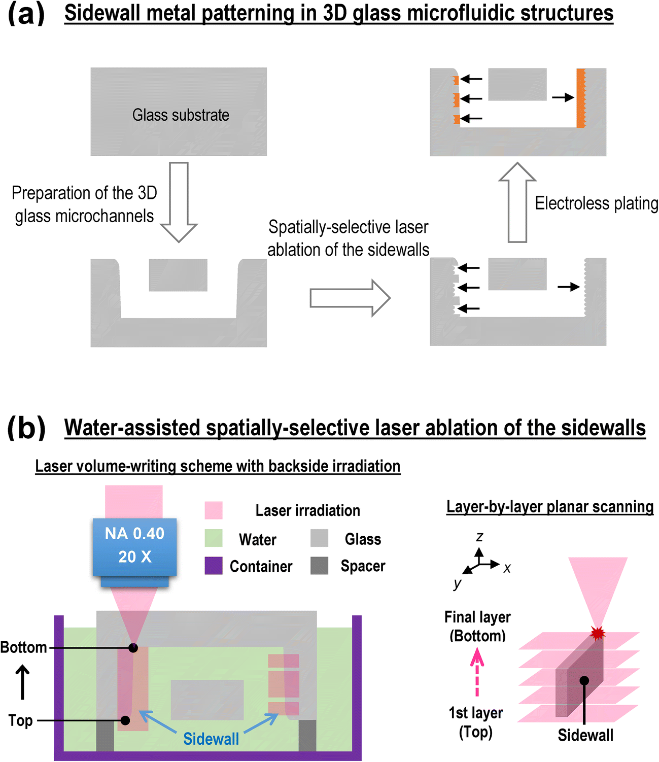 | ||
| Fig. 1 (a) Schematic of the procedure for sidewall metal patterning in 3D glass microfluidic structures, which consists of three main steps: preparation of the 3D glass microchannels followed by spatially-selective laser ablation of the microchannel sidewalls and subsequent electroless plating. (b) Schematic of water-assisted laser ablation of microchannel sidewalls. The water is always in contact with the ablated region. The laser volume-writing scheme (layer-by-layer planar scanning) from the top to the bottom of the sidewall was employed using focused laser irradiation from the backside of the substrate for full-height ablation of the sidewall. Spatially-selective ablation of the sidewall can be achieved by programming the writing scheme. | ||
Worm culture and electrotaxis experiments
Wild-type C. elegans (N2 strain) were cultured on nematode growth medium (NGM) agar plates seeded with the OP50 strain of Escherichia coli at 16 °C according to standard methods.39,40 In most of the electrotaxis experiments, young adult animals were used. Before the experiments, the worms were transferred with a worm pick from the NGM plates to PCR tubes containing M9 buffer (3 g KH2PO4, 6 g Na2HPO4, 5 g NaCl, 1 ml 1 M MgSO4, H2O to 1 L). Then, the worms were loaded into microreservoirs in electrofluidic glass chips using a pipette. The electric field of the electrofluidic devices was provided by an external DC supply (Kikusui Electronics Corp., PMC 35-2A). For the electrical interconnections in the electrofluidic devices, conventional conductive copper wires were bonded to recessed electrode pads fabricated on the glass substrate surfaces using a silver paste (Epoxy Technology, Inc., EPO-TEK® H20E). The entire surfaces of the internal walls of the microfluidic structures were coated with a thin film of polymer by dip-coating with a mixture of SU8 solution (Microchem Corp., SU8-2050) and acetone at a volume ratio of 1![[thin space (1/6-em)]](https://www.rsc.org/images/entities/char_2009.gif) :30 followed by baking for 30 min at 90 °C to electrically isolate the formed metal structures.
:30 followed by baking for 30 min at 90 °C to electrically isolate the formed metal structures.
Results and discussion
Water-assisted laser direct-write ablation for improving volumetric controllability and processing precision in micropatterning
To explore the effects of the introduction of water, sidewall ablation using the laser volume-writing scheme36 shown in Fig. 1(b) with an irradiated volume of ∼100(x) × 50(y) × 500(z) μm3 (line-by-line scan speed: 200 μm s−1, scan spacing: 3 μm; layer-by-layer scan pitch: 10 μm, scan distance in the z direction: ∼330 μm) was performed at different pulse energies without (in air) and with water assistance. As observed on the 500 μm-high sidewall surface of the open microreservoir shown in Fig. 2, the ablated volume increases with pulse energy (right to left). Above a pulse energy of 2.5 μJ, almost the entire area of the laser-irradiated sidewall surfaces was ablated in both cases. However, the volume of the laser removed regions for the water-assisted ablation was significantly larger and the morphology and shapes (especially the edges) of the ablated structures were much better than those achieved through ablation in air (Fig. S1, ESI†). For a clearer observation, the regions for the pulse energy of 3 μJ indicated by the dashed regions in Fig. 2(a) and (b) are enlarged in Fig. 2(c) and (d), respectively. The dashed arrowed lines in Fig. 2(c) and (d) correspond to the inner boarders of grooves ablated without and with water, respectively. It is apparent that the water assistance creates much deeper grooves with a higher surface quality and sharper edges. The ablated depth of the groove in the laser scanning direction (x) on the bottom of the microreservoir in Fig. 2(d) was measured to be ∼85 μm, which corresponds to the designed scanning length of the focused laser beam in glass sidewall (∼70 μm) in the x-direction plus an ablated length of ∼15 μm on the bottom of the reservoir in water on the final layer (the total scanning length was ∼100 μm; a scanning length of ∼15 μm on the bottom of the reservoir was not ablated in this case). This result indicates that the laser irradiated regions of the glass sidewall are almost completely removed (Fig. S1, ESI†). This was also confirmed through the observation of bubbles generated by the focused laser beam in the water during the processing, because in situ generated bubbles can be observed when the water makes contact with the ablated surface. In the water-assisted ablation, a pulse energy of 3 μJ is high enough to create the controllable ablated patterns on a 500 μm high sidewall without debris redeposition. Further increase of pulse energy may generate micro-cracks around the edges of ablated structures. Additionally, nonlinear propagation such as filamentation may affect the processing precision and then degrade quality of fabricated structures.41–43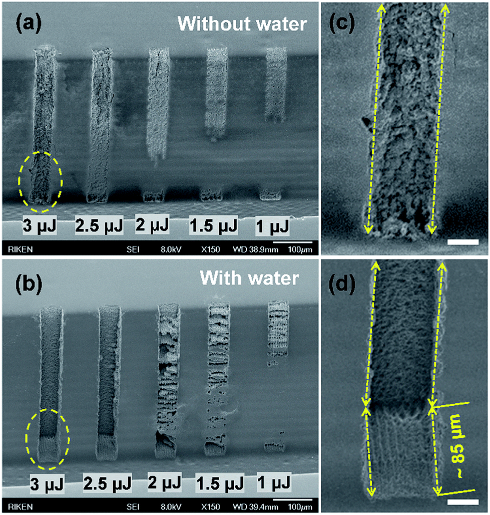 | ||
| Fig. 2 45°-tilted SEM images of ablated regions formed on the 500 μm-high sidewall surface of an open microreservoir using the laser volume-writing scheme with different pulse energies (a) without and (b) with the introduction of water; (c) and (d) magnified SEM images (45°-tilted view) of the regions of the 50 μm-width grooves indicated by the dashed outlines in (a) and (b), respectively, for a pulse energy of 3 μJ. The dashed arrowed lines in (c) and (d) indicate the inner borders of the formed structures after laser ablation, clearly showing the improved volume removal in (d) compared with that in (c). The scale bar in (c) and (d) is 25 μm. | ||
Although, strictly speaking, the sidewalls of the open microfluidic structures such as microreservoirs and channels prepared by fs-laser modification followed by chemical etching and additional annealing process are not vertical (Fig. S2, ESI†) due to longer exposure time to hydrofluoric acid solutions44–46 and different melting behavior during annealing process at the regions closer to the top of sidewall compared with the bottom. We found that the water-assisted ablation method produces reconstructed sidewalls that are nearly perpendicular to the bottom of the microreservoir (see Fig. S2 in the ESI†). This feature is very important in terms of fabricating sidewall electrodes that create a uniform electric field in the microfluidic channel. Researchers have shown that bubbles, high-speed jets and shock waves produced in water by a focused laser beam can force the generated debris out of the focused volume and greatly reduce the extent of blocking and redeposition.42,47–49 With these effects in mind, we discuss a mechanism through which the high-efficiency, high-quality etching using water-assisted sidewall ablation may occur. At the beginning of the volume-writing scanning, the laser beam is focused in the water, resulting in the generation of bubbles. Sidewall ablation (and the production of debris) starts occurring as soon as the scanning laser beam arrives at the sidewall surface. The debris produced is efficiently removed from the ablated surface due to the formation of bubbles, high-speed jets and shock waves and thus redeposition on the ablated surface does not occur. As a result, the ablated surface is continuously exposed to water and the generation of bubbles, high-speed jets and shock waves is self-maintained. This efficient removal of debris from the ablated surface continues until the volume-writing scheme ends. In contrast, the redeposition of debris that occurs during ablation in air inhibits further ablation, resulting in a much smaller ablated volume. Another advantage of using water is minimizing the refractive index (n) mismatch at the glass sidewall surface–air interface (nglass ≈ 1.5, nwater ≈ 1.3 and nair ≈ 1), leading to higher quality of laser ablation. In some cases, the effect of continuously generating bubbles in microfluidic structures may hinder debris ejection in subsequent laser ablation processes, but this can be overcome by introducing a fresh flow of water50 or ultrasonic wave agitation.42
The unique advantage of water-assisted fs-laser direct-write ablation is that it can be used to create micropatterns with tailored sizes and volumes in addition to flexibly controlling the shapes of structures formed on sidewalls in a spatially-selective manner. For example, an O-shaped pattern with a very well-defined edge can be ablated on the sidewall surface (Fig. 3(a) and S3 in the ESI†). The processing speed for straight pattern fabrication on a 500 μm-high sidewall can reach the order of mm s−1 with a pulse energy of 2.5 μJ, as shown in Fig. 3(b). By designing an appropriate laser scanning scheme for the volume writing, the letters “LOC” were ablated on sidewalls at arbitrary positions with different sizes and volumes, as presented in Fig. 3(c) and (d). Although laser direct-write ablation in air can homogeneously ablate sidewalls, as is done for forming electrical interconnections into microchannels, the volumetric controllability and processing precision achieved by water-assisted laser processing is clearly superior.
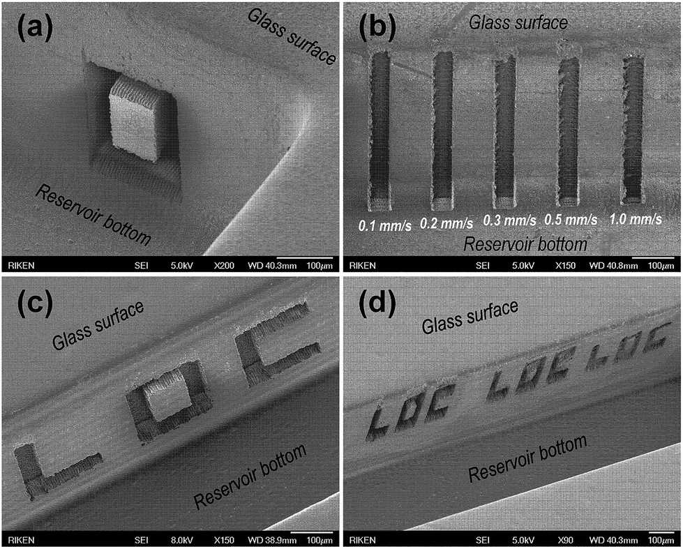 | ||
| Fig. 3 Water-assisted fs-laser direct-write ablated micropatterns formed on the 500 μm-high sidewall surface of an open microreservoir. 45°-tilted SEM images of (a) an O-shaped pattern and (b) five vertical grooves formed with different writing speeds; (c) 30°-tilted SEM image of an ablated “LOC” logo; (d) 45°-tilted SEM image of ablated “LOC” logos with different sizes and volumes. | ||
Highly flexible sidewall metal patterning
Although the introduction of water during laser processing greatly improves the ablation quality compared with that carried out in air (see Fig. 2(c) and (d)), the ablated surfaces are still sufficiently rough for selective metallization. Selective metal deposition on laser-ablated patterns of different sizes through electroless plating was demonstrated as shown in Fig. 4. A comparison with the structure before plating (see Fig. 3(c)) confirmed that the metal films were selectively deposited onto the laser-modified regions (see Fig. 4(a)–(c) and S4 in the ESI†). Although the deposited metal structures did not fully fill the ablated regions as shown in Fig. 4(a)–(c), further improvements to the electroless plating process such as optimizing the plating time and composition of the plating solution will improve the deposition characteristics.51,52 Furthermore, it is not difficult to reduce the widths of the metallized micropatterns on the sidewall surface to several tens of microns (see Fig. 4(d) and S4 in the ESI†). Such a flexible metal patterning method for the sidewalls of microfluidic structures may provide a new means of realizing highly controllable lateral electric fields in microfluidic channels, which can be utilized in many biochip applications.30–32 In addition, through electroless copper plating, a uniform and continuous metal pad can be selectively deposited onto the laser-modified sidewall of a glass microreservoir as well as the glass surface, as shown in Fig. 4(e) and its inset, respectively. The recessed structure on the top of the sidewall shown in the figure was created by laser ablation of the glass surface and can be used for the formation of a metal connecting line on the glass surface. Additional electroless gold plating of the sample in Fig. 4(e) can be performed while maintaining a high degree of selectivity.36 As can be seen in Fig. 4(f), in which the metalized sample is tilted by ∼80°, thin gold films completely cover the copper films formed on both the ablated surface (see the inset of Fig. 4(f)) and the sidewall (Fig. 4(f)) with high selectivity. This metallization is used to form an electrical interconnection (see Fig. S5 in the ESI†). The vertical sidewall electrode (∼500 μm high, ∼800 μm wide, ∼10 μm thick) formed using this technique can generate a homogeneous electric field in the microfluidic channel, with the power provided externally via the electrical pads formed on the glass surface. It is noted that although the above-mentioned sidewall metal patterning was presented in an open microreservoir environment for direct observation and convenient characterization, selective metal deposition on the sidewalls of closed and multi-layered microfluidic structures is also possible for both fs-laser modification and electroless plating due to the unique capabilities this method offers.36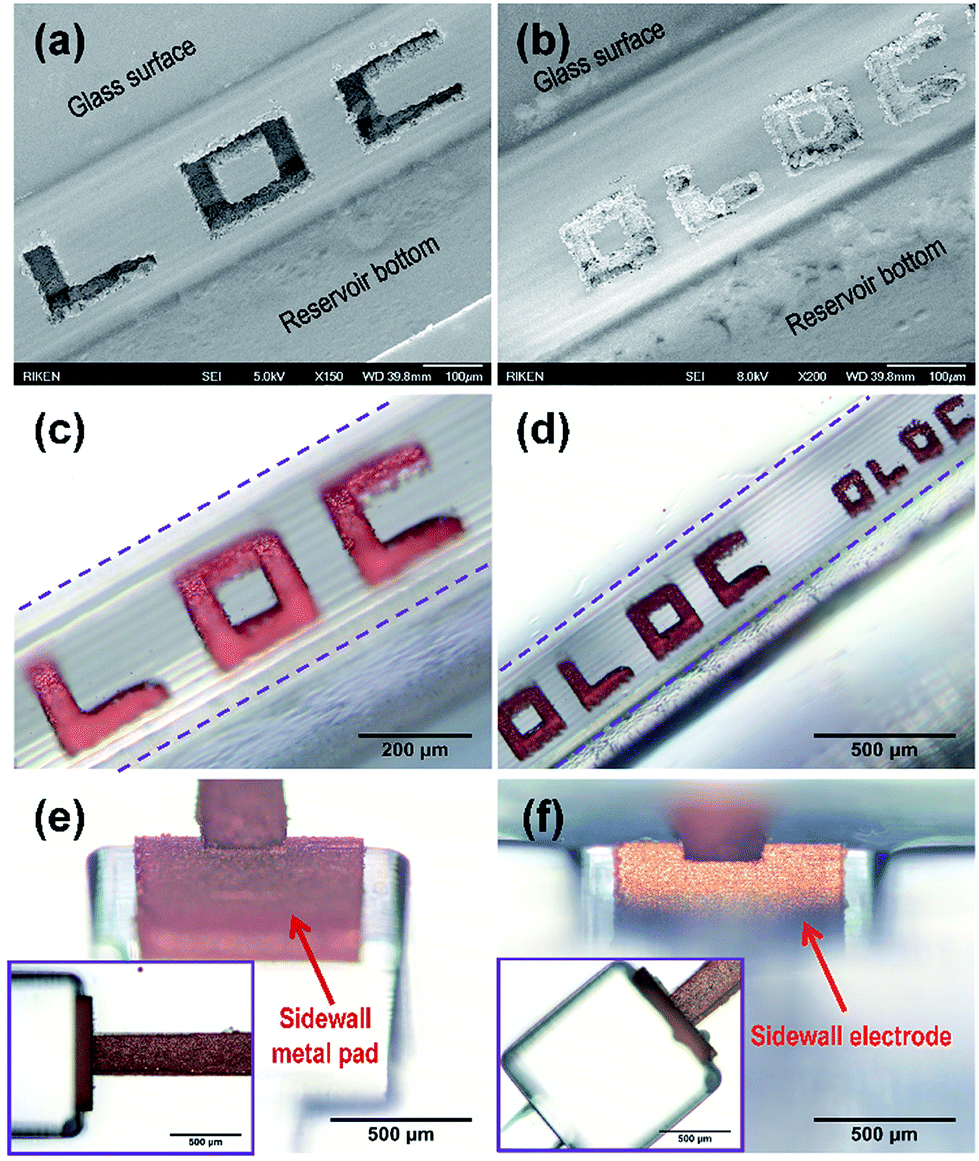 | ||
| Fig. 4 30°-tilted ((a) and (b)) SEM images and 45°-tilted ((c) and (d)) optical microscope images of selective metal deposition on laser-ablated patterns (the letters “LOC” and “OLOC”) formed on sidewall surfaces after electroless copper plating. The two dashed lines in (c) and (d) indicate the sidewall edges. (e) Optical microscope image of a metal pad formed on a sidewall surface after electroless copper plating. The sidewall surface is tilted by ∼45° with respect to the direction of observation. The inset is a top-down view of continuous metal patterning from the glass surface through the sidewall to the bottom of the microreservoir. (f) Optical microscope image of the sidewall metal pad in (e) after additional gold plating. The sidewall surface is tilted by ∼80° with respect to the direction of observation. The vertical sidewall electrode has an aspect ratio (height/thickness) of ∼50. The inset is a top-down view of the final metal patterns. The recessed structures observed on the top of the sidewalls in (e) and (f) were created by laser ablation to produce metal interconnections on the glass surface. The height of all sidewalls shown is ∼500 μm. | ||
It's well known that water-assisted fs laser ablation of glass has been established as one of the most popular techniques to prepare high aspect-ratio microchannels even nanoscale channels in the past decades.42,43,47–49 But the surfaces of internal walls of microfluidic channels prepared by the water-assisted fs laser ablation are significantly roughened as compared with those prepared by our 3D glass micromachining technique combined with post-annealing.37 To the best of our knowledge, it is for the first time to apply this differentiation of surface roughness between two techniques for developing flexible metal patterning in 3D microchannels. Particularly, the vertical sidewall electrode with a high aspect ratio can be prepared in a facile manner. Secondly, the controllability and flexibility of sidewall metal patterning has been significantly improved, enabling us to obtain the designable metal patterns with different sizes and positions on the sidewalls even in a closed microfluidic structures. Such improvements with the feature of in-channel integration of metal patterns rely on the nonlinear nature of fs laser microfabrication and involvement of water's assistance. Namely, the focused laser beam is capable of selectively roughening the specific areas in the internal surface of microchannels without changing the properties of the regions of glass where the laser beam is transmitted. As another important point, in addition to the effective removal of debris, the water can reduce the refractive index mismatch between air and glass and then improve the focusing condition at the interface for better processing quality of structured surface.
In situ control of electrotaxis in a chip using vertical electrodes
The fabricated sidewall electrodes can be monolithically integrated into microfluidic structures to form electrofluidic structures in glass for the electrical manipulation of biological samples. As seen in Fig. 5(a), an electrofluidic glass chip in which two metal pads was formed on glass surface and the walls of two open microreservoirs (∼1.2 × 1.2 × 0.5 mm3 in size) connected by an embedded microchannel (∼300 μm wide, ∼100 μm high and ∼3.3 mm long) was prepared (Fig. S5, ESI†). To generate a laterally homogeneous electric field along the microchannel, the width of the sidewall electrodes (∼800 μm, see Fig. 4(f) and 5(b)) is larger than that of the channel shown in the bottom inset of Fig. 5(a). The sidewall electrodes with heights of ∼500 μm can be clearly seen with the angled view used to take the photograph shown in Fig. 5(b). An electrofluidic chip of this sort is applicable to manipulate the electrotaxis of the nematode (worm) C. elegans. First, electrical isolation by coating the electrofluidic structure with an SU8 layer is performed as described before. To investigate the effects of an applied electric force other than random omnidirectional swimming of a worm in the microchannel, the change in direction of the C. elegans was examined while switching the polarity of the electric field in the microchannel during the observation (see the Movie in ESI†). When a DC electric field (−3.5 V cm−1) was applied between the two electrodes on the sidewalls (left electrode: negative voltage, right electrode: positive voltage), the C. elegans in the microchannel swam from the right to the left with the electric field as indicated by the arrow on the left of Fig. 5(c) (t = 0 s). After ∼7.5 s, the polarity of the electric field was switched (see bottom-left snapshot of Fig. 5(c)). The worm was then observed to rotate its body and swim from the left to the right in the direction of the new electric field, clearly demonstrating controllable electrotaxis behavior.13,25 Furthermore, the worm was still swimming to the right at ∼12.5 s, because the electric field remained in that direction. Thus, we confirmed that the worm always swims towards the negative electrode and succeeded in manipulating its swimming behavior.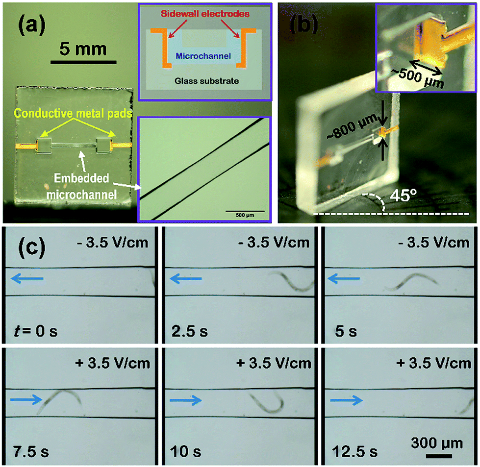 | ||
| Fig. 5 (a) Photograph of an electrofluidic glass chip in which two metal pads were formed on the surface and the walls of two open microreservoirs connected by an embedded microchannel. The top and bottom insets show a schematic cross-sectional view of the electrode structure in glass and an optical microscope image of the microchannel, respectively. (b) Photograph of the on-chip sidewall electrode in (a) taken at an angle of 45°. The inset shows a close-up of the electrode. (c) Observation of a C. elegans worm changing its direction in the microchannel using the on-chip electrofluidics in (a) when the polarity of an electric field (∼3.5 V cm−1) was switched at ∼7.5 s. The arrow in each in situ snapshot image indicates the direction of the electric field. | ||
The optimum applied DC voltage for electrotaxis of the worms performed in this work is about 2 V. Beyond this value, the generation of bubbles at the surface of the sidewall electrodes will occur and then degrade the electrodes. We assume it is ascribed to electrical breakdown of SU8 isolation layers covering the electrodes. Using better insulating material may improve this characteristic to achieve higher electric fields, which will be explored in the near future.
Previous work using the wire-based method for electrotaxis in microfluidics allowed to provide the intensity of electric field in the microchannels as high as ∼10 V cm−1.14 However, considering the stability of positioning of the wires, robust on-chip integration of electrodes is highly desirable. Furthermore, the flexibility for tailoring the spatial distribution of electric field in microchannels using wire electrodes is not high, e.g., for application to 3D multi-layered sorting devices with a spatial-selective control. In contrast, the electrodes prepared by our technique can get rid of aforementioned limitations. First, the designable contact area of the electrode can be as large as one requires since electrode width can be easily tuned by laser direct-write scheme. For the wire-based method, the diameter of the wires for electrotaxis are typically 0.5–0.8 mm which result in contact areas of more than 0.15 mm2. Although it is comparable to the sidewall electrodes with a contact area of 0.4 mm2 (∼500 μm high, ∼800 μm wide) used in this study, using the technique proposed here is no technical limitation to achieve a contact area over 1 mm2 depending on the proper laser ablation scheme (e.g., ∼500 μm high, ∼2500 μm wide). Secondly, the space-selective installation of electrodes is feasible to produce selective control of electrotaxis in specific microfluidic channels and environments. In principle, this technique can be used to create vertical electrodes at any position in closed or even multi-layered microfluidic structures, allowing environments unmatched in terms of their flexibility and manipulability of biological samples to be realized.
In addition, the electrodes prepared by this technique have good adhesion on the glass surfaces as well as internal surface of microchannels as shown in our previous work36 for ensuring the stability of installed electrodes. The deposited metal films on the sidewalls of glass microreservoirs were not peeled off during the operation of the electrotaxis experiments and the fabricated electrofluidic devices with integrated vertical electrodes could be repeatedly used for electrotaxis experiments. It should be noted that, the electrodes fabricated without water-assistance can be also used for electrotaxis of C. elegans under the same electric-field intensity (∼3.5 V cm−1). However, in the case of without the water-assistance, the electrodes were formed on the areas where residual debris were redeposited, which may lead to instability of device for the repeated operation with the applied DC electric field. In contrast, the water-assisted fabrication can fully remove the debris, which provides superior stability for repeated use of electrodes as already demonstrated. Furthermore, we believe that vertical electrodes prepared by water-assisted fabrication can precisely control the distribution of electric-field intensity in complicated or even multi-layered 3D microfluidic structures, which is necessary to guarantee the precise and flexible manipulation of bio-samples in the complex system. Considering the demonstration as a proof-of-principle for the electrotaxis experiments presented in this paper, more critical applications of vertical sidewall electrodes enabling flexible control of distribution of electric field in closed microfluidic channels with 3D complicated geometries will be expected.
Conclusion
Sidewall metal patterning in 3D glass microfluidic structures, specifically the facile fabrication of vertical sidewall electrodes with high aspect ratios, has been achieved by employing water-assisted fs-laser direct-write ablation followed by electroless plating. The introduction of water into the laser ablation process greatly improves the removal of debris, leading to a higher quality of ablated micropatterns and enhancing the flexibility and precision of the metal patterning for electroless plating as a result. Accordingly, sidewall metal micropatterns with a controllable geometry and feature size, specifically sidewall electrodes 500 μm in height and almost any width, can be prepared far more easily in comparison with conventional techniques. Monolithic integration of sidewall electrodes into microfluidic components provides a simple means of creating electrofluidic glass chips, with which electrotaxis experiments on C. elegans were performed. Among the existing techniques for fabrication of sidewall metal electrodes in microfluidic devices, a conventional strategy of multiple layer photolithography combined with metal deposition and electroplating offers a high-precision, high-quality electrode integration with parallel processing capability for microfluidic application.26–28 Nevertheless, this strategy requires tedious fabrication steps, rigorous alignment and bonding procedures. Injection of liquid metals or conductive composites into microchannels30–32 provides a fast and facile method to integrate well aligned electrodes into microfluidic devices. However, it has some limitations on mechanical stability and achievable electrode geometries along the sidewalls of microchannels. More recently, an intermediate bonding layer has been applied to lower the fusion bonding temperature of glass materials to achieve coplanar side electrode pairs integrated at the half height of the microchannels.34 Although this method has an ability to place the side electrodes at any position on the glass microchip without blocking the optical visibility, multiple photolithographic processes are still required. In contrast, the proposed method which only employs water-assisted fs laser direct write combined with subsequent electroless metal plating provides a simple, easy, bonding-free way for preparation of designable vertical electrodes with high-flexibility. Moreover, the fs laser direct write technique offers the capability of integrating other functions such as microoptics for optofluidic integration in glass,37 which is still difficult by most of the other fabrication techniques. Considering the 3D capabilities of the fs-laser direct-write technique, the integration of optical sensing and photonic functions such as optical waveguides53–56 and optical fibers57 with electrofluidic structures that have 3D designable configurations into a single glass substrate will make possible more dynamic and complex electrical manipulation of biological samples in 3D microfluidic spaces with feedback control for novel lab-on-a-chip applications. Additionally, this sidewall metal patterning technique has the potential to be extended to other transparent substrates such as fused silica, where the space-selective patterning of catalysis seeds on microfluidic structures using fs-laser assisted modification can be performed.58–60Acknowledgements
This work was supported by JSPS KAKENHI Grant Number 25286038. The authors would like to thank Prof. Ya Cheng in Shanghai Institute of Optics and Fine Mechanics and Dr Xiaofeng Liu in Zhejiang University for discussions regarding this work.Notes and references
- J. El-Ali, P. K. Sorger and K. F. Jensen, Nature, 2006, 442, 403–411 CrossRef CAS PubMed.
- L. Y. Yeo, H.-C. Chang, P. P. Y. Chan and J. R. Friend, Small, 2011, 7, 12–48 CrossRef CAS PubMed.
- E. K. Sackmann, A. L. Fulton and D. J. Beebe, Nature, 2014, 507, 181–189 CrossRef CAS PubMed.
- A. Ben-Yakar, N. Chronis and H. Lu, Curr. Opin. Neurobiol., 2009, 19, 561–567 CrossRef CAS PubMed.
- N. Chronis, Lab Chip, 2010, 10, 432–437 RSC.
- D. R. Albrecht and C. I. Bargmann, Nat. Methods, 2011, 8, 599–605 CrossRef CAS PubMed.
- W. Shi, H. Wen, B. Lin and J. Qin, Top. Curr. Chem., 2011, 304, 323–338 CrossRef CAS.
- N. A. Bakhtina and J. G. Korvink, RSC Adv., 2014, 4, 4691–4709 RSC.
- X. Ding, S. S. Lin, B. Kiraly, H. Yue, S. Li, I.-K. Chiang, J. Shi, S. J. Benkovic and T. J. Huang, Proc. Natl. Acad. Sci. U. S. A., 2012, 109, 11105–11109 CrossRef CAS PubMed.
- J. Li and F. Lin, Trends Cell Biol., 2011, 21, 489–497 CrossRef CAS PubMed.
- Y. Hanada, K. Sugioka, I. S. Ishikawa, H. Kawano, A. Miyawaki and K. Midorikawa, Lab Chip, 2011, 11, 2109–2115 RSC.
- K. Ozasa, J. Lee, S. Song, M. Hara and M. Maeda, Lab Chip, 2011, 11, 1933–1940 RSC.
- C. V. Gabel, H. Gabel, D. Pavlichin, A. Kao, D. A. Clark and A. D. T. Samuel, J. Neurosci., 2007, 27, 7586–7596 CrossRef CAS PubMed.
- P. Rezai, A. Siddiqui, P. R. Selvaganapathy and B. P. Gupta, Lab Chip, 2010, 10, 220–226 RSC.
- P. Rezai, A. Siddiqui, P. R. Selvaganapathy and B. P. Gupta, Appl. Phys. Lett., 2010, 96, 153702 Search PubMed.
- P. Rezai, S. Salam, P. R. Selvaganapathy and B. P. Gupta, Biomicrofluidics, 2011, 5, 044116 CrossRef PubMed.
- X. Manière, F. Lebois, I. Matic, B. Ladoux, J.-M. Di Meglio and P. Hersen, PLoS One, 2011, 6, e16637 Search PubMed.
- J. A. Carr, R. Lycke, A. Parashar and S. Pandey, Appl. Phys. Lett., 2011, 98, 143701 Search PubMed.
- C.-W. Huang, J.-Y. Cheng, M.-H. Yen and T.-H. Young, Biosens. Bioelectron., 2009, 24, 3510–3516 CrossRef CAS PubMed.
- H.-S. Chuang, D. Raizen, A. Lamb, N. Dabbish and H. Bau, Lab Chip, 2011, 11, 599–604 RSC.
- B. Han, D. Kim, U. H. Ko and J. H. Shin, Lab Chip, 2012, 12, 4128–4134 RSC.
- J. A. Carr, A. Parashar, R. Gibson, A. P. Robertson, R. J. Martin and S. Pandey, Lab Chip, 2011, 11, 2385–2396 RSC.
- Y.-S. Sun, S.-W. Peng and J.-Y. Cheng, Biomicrofluidics, 2012, 6, 034117 CrossRef PubMed.
- J. Li, S. Nandagopal, D. Wu, S. F. Romanuik, K. Paul, D. J. Thomson and F. Lin, Lab Chip, 2011, 11, 1298–1304 RSC.
- P. Rezai, S. Salam, P. R. Selvaganapathy and B. P. Gupta, Lab Chip, 2012, 12, 1831–1840 RSC.
- L. Wang, L. A. Flanagan and A. P. Lee, J. Microelectromech. Syst., 2007, 16, 454–461 CrossRef CAS.
- L. Wang, L. A. Flanagan, N. L. Jeon, E. Monuki and A. P. Lee, Lab Chip, 2007, 7, 1114–1120 RSC.
- W. C. Chang and D. W. Sretavan, Biosens. Bioelectron., 2009, 24, 3600–3607 CrossRef CAS PubMed.
- J. W. Choi, S. Rosset, M. Niklaus, J. R. Adleman, H. Shea and D. Psaltis, Lab Chip, 2010, 10, 783–788 RSC.
- A. Pavesi, F. Piraino, G. B. Fiore, K. M. Farino, M. Moretti and M. Rasponi, Lab Chip, 2011, 11, 1593–1595 RSC.
- J.-H. So and M. D. Dickey, Lab Chip, 2011, 11, 905–911 RSC.
- S. Li, M. Li, Y. S. Hui, W. Cao, W. Li and W. Wen, Microfluid. Nanofluid., 2013, 14, 499–508 CrossRef CAS.
- B. Mustin and B. Stoeber, Lab Chip, 2012, 12, 4702–4708 RSC.
- S. Sukas, E. Schreuder, B. de Wagenaar, J. Swennenhuis, A. van den Berg, L. Terstappen and S. Le Gac, Lab Chip, 2014, 14, 1821–1825 RSC.
- P. Benhal, J. G. Chase, P. Gaynor, B. Oback and W. Wang, Lab Chip, 2014, 14, 2717–2727 RSC.
- J. Xu, D. Wu, Y. Hanada, C. Chen, S. Wu, Y. Cheng, K. Sugioka and K. Midorikawa, Lab Chip, 2013, 13, 4608–4616 RSC.
- K. Sugioka and Y. Cheng, Lab Chip, 2012, 12, 3576–3589 RSC.
- Y. Hanada, K. Sugioka and K. Midorikawa, Appl. Phys. A: Mater. Sci. Process., 2008, 90, 603–607 CrossRef CAS.
- S. Brenner, Genetics, 1974, 77, 71–94 CAS.
- T. Stiernagle, Maintenance of C. elegans WormBook, ed. The C. elegans Research Community, WormBook, 11 February 2006, DOI:10.1895/wormbook.1.101.1, http://www.wormbook.org.
- Z. Wu, H. Jiang, L. Luo, H. Guo, H. Yang and Q. Gong, Opt. Lett., 2002, 27, 448–450 CrossRef CAS.
- D. J. Hwang, T. Y. Choi and C. P. Grigoropoulos, Appl. Phys. A: Mater. Sci. Process., 2004, 79, 605–612 CrossRef CAS PubMed.
- R. An, Y. Li, Y. Dou, H. Yang and Q. Gong, Opt. Express, 2005, 13, 1855–1859 CrossRef.
- M. Masuda, K. Sugioka, Y. Cheng, N. Aoki, M. Kawachi, K. Shihoyama, K. Toyoda, H. Helvajian and K. Midorikawa, Appl. Phys. A: Mater. Sci. Process., 2003, 76, 857–860 CrossRef CAS.
- Y. Bellouard, A. Said, M. Dugan and P. Bado, Opt. Express, 2004, 12, 2120–2129 CrossRef CAS.
- K. C. Vishnubhatla, N. Bellini, R. Ramponi, G. Cerullo and R. Osellame, Opt. Express, 2009, 17, 8685–8695 CrossRef CAS.
- Y. Li, K. Itoh, W. Watanabe, K. Yamada, D. Kuroda, J. Nishii and Y. Jiang, Opt. Lett., 2001, 26, 1912–1914 CrossRef CAS.
- Y. Liao, Y. Ju, L. Zhang, F. He, Q. Zhang, Y. Shen, D. Chen, Y. Cheng, Z. Xu, K. Sugioka and K. Midorikawa, Opt. Lett., 2010, 35, 3225–3327 CrossRef PubMed.
- C. Liu, Y. Liao, F. He, J. Song, D. Lin, Y. Cheng, K. Sugioka and K. Midorikawa, J. Laser Micro/Nanoeng., 2013, 8, 170–174 CrossRef.
- Y. Li and S. Qu, Opt. Lett., 2011, 36, 4236–4238 CrossRef CAS PubMed.
- Y. Liao, J. Xu, H. Sun, J. Song, X. Wang and Y. Cheng, Appl. Surf. Sci., 2008, 254, 7018–7021 CrossRef CAS PubMed.
- Z. Wang, O. Yaegashi, H. Sakaue, T. Takahagi and S. Shingubara, J. Electrochem. Soc., 2004, 151, C781–C785 CrossRef CAS PubMed.
- R. Osellame, H. J. W. M. Hoekstra, G. Cerullo and M. Pollnau, Laser Photonics Rev., 2011, 5, 442–463 CrossRef CAS.
- A. Schaap, T. Rohrlack and Y. Bellouard, Lab Chip, 2012, 12, 1527–1532 RSC.
- Z. Wang, K. Sugioka, Y. Hanada and K. Midorikawa, Appl. Phys. A: Mater. Sci. Process., 2007, 88, 699–704 CrossRef CAS PubMed.
- Y. Hanada, K. Sugioka and K. Midorikawa, Lab Chip, 2012, 12, 3688–3693 RSC.
- Y. Cheng, K. Sugioka and K. Midorikawa, Opt. Express, 2005, 13, 7225–7232 CrossRef CAS.
- J. Xu, Y. Liao, H. Zeng, Z. Zhou, H. Sun, J. Song, X. Wang, Y. Cheng, Z. Xu, K. Sugioka and K. Midorikawa, Opt. Express, 2007, 15, 12743–12748 CrossRef CAS.
- Y. Liao, L. Qiao, Z. Wang, M. Wang, L. Liu, K. Sugioka and Y. Cheng, Opt. Mater. Express, 2013, 3, 1698–1704 CrossRef.
- J. Song, Y. Liao, C. Liu, D. Lin, L. Qiao, Y. Cheng, K. Sugioka, K. Midorikawa and S. Zhang, J. Laser Micro/Nanoeng., 2012, 7, 334–338 CrossRef CAS.
Footnote |
| † Electronic supplementary information (ESI) available: A flowchart of sidewall metal patterning in glass microfluidic structures. Fig. S1–S5 related on water-assisted femtosecond-laser fabrication and subsequent electroless plating of sidewalls. A movie of the in situ control of electrotaxis of C. elegans and subsequent electroless plating of sidewalls using an electrofluidic device. See DOI: 10.1039/c5ra00256g |
| This journal is © The Royal Society of Chemistry 2015 |