
Specific features of electronic structures and optical susceptibilities of molybdenum oxide†
A. H. Reshak*ab
aNew Technologies – Research Centre, University of West Bohemia, Univerzitni 8, 306 14 Pilsen, Czech Republic. E-mail: maalidph@yahoo.co.uk; Tel: +420 777729583
bCenter of Excellence Geopolymer and Green Technology, School of Material Engineering, University Malaysia Perlis, 01007 Kangar, Perlis, Malaysia
First published on 9th February 2015
Abstract
Orthorhombic molybdenum trioxide, α-MoO3, is comprehensively investigated using density function theory based on the all-electron full potential linear augmented plane wave (FPLAPW) method as implemented in the WIEN2k code within four types of exchange correlation potentials, namely, the local density approximation (CA-LDA), generalized gradient approximation (PBE-GGA), Engel–Vosko generalized gradient approximation (EVGGA) and the modified Becke–Johnson potential (mBJ). The conduction band minimum (CBM) is situated at Γ point of Brillouin zone (BZ), whereas the valence band maximum (VBM) is located at T point of BZ. Calculation demonstrated that α-MoO3 is an indirect band gap insulator. The calculated electronic band structure and the total density of states confirm that mBJ brings the calculated energy band gap (2.81 eV) closer to the experimental one (3.03, 3.10 eV). The electronic space charge density distribution of α-MoO3 is explored in two crystallographic planes, namely, (0 0 1) and (1 0 1), to scrutinize the origin of chemical bonds. It is found that the majority of the charges are accumulated on the O site and the distribution of electronic charge is spherical. The optical properties are calculated for three tensor components along the polarization directions [1 0 0], [0 1 0] and [0 0 1] with respect to the crystalline axes. It is found that the regions confined between 6.5 and 8.0 eV and 10.0 and 13.5 eV are considered as lossless regions. The calculated optical properties support our observation from the calculated electronic band structure and the density of states, which shows that LDA, GGA and EVGGA underestimate the energy band gap, while mBJ succeeds by a large amount in bringing the calculated energy band gap closer to the experimental one.
1. Introduction
Recent studies confirm that transition metal oxides such as molybdenum trioxide (MoO3) have attracted great interest due to their excellent chemical and physical properties. MoO3 is useful for numerous applications1–5 in electrochromic display devices, optical memories, as a cathode material in the development of high-energy density solid-state microbatteries, gas sensors and lithium batteries due to its wide range of stoichiometries and interesting behavior, which includes chromogenic and catalytic properties. The main application of molybdenum trioxide is as a raw material for the production of molybdenum metal and as an oxidation catalyst. Moreover, it is used as an additive in steel and other corrosion-resistant alloys, as an industrial catalyst, a pigment, a crop nutrient, a component of glass, a flame retardant for polyester and polyvinyl chloride resins, chemical reagent and in ceramics and enamels. Therefore, molybdenum trioxide has many scientific and technological applications. MoO3 is a 4d0Mo(VI) compound, and it is decomposed into other molybdenum oxide compounds.6 α-MoO3 is an insulator with a band gap of 3.1 eV.6 Klinbumrung et al.7 produced orthorhombic α-MoO3 microplates from (NH4)6Mo7O24·4H2O solid powder using a 900 W microwave plasma for 40, 50, and 60 min. They reported that α-MoO3 is a wide bandgap n-type semiconductor.Molybdenum trioxide exists in orthorhombic structure α-MoO3 (thermodynamically stable),8,9 monoclinic structure β-MoO3 (metastable),10 high pressure monoclinic structure MoO3-II11 and hexagonal structure h-MoO3.12,13 α-MoO3 is the most stable phase at the normal conditions.8,9 Atuchin et al.14 have grown high-quality platelet α-MoO3 single crystals with dimensions of 1000 × 200 × 0.4 μm3 on Si (100) substrates in a quartz tube reactor in air atmosphere by the sublimation of molybdenum oxide at T = 660 °C. The phase composition of grown crystals was identified by X-ray single crystal structure analysis.
The layered structure of α-MoO3 (orthorhombic phase) consists of double corner-sharing layers of MoO6 octahedra held together by covalent forces along (100) and (001) directions and by van der Waals forces along (010) direction.19 The octahedra have one short Mo–O bond to non-bridging O. α-MoO3 is a yellow or light blue colored crystalline solid that is slightly soluble in acid water.6
As mentioned above, it is clear that the previous work were devoted to the synthesis α-MoO3 and study of their crystal structure, electronic properties, energy band gap, and chemical bonding; however, there were no reports on the electronic band structure therefore, due to a lack of information regarding the electronic band structure, density of states, electronic charge density distribution and the linear optical properties of α-MoO3, we addressed ourselves to comprehensive theoretical calculations based on density functional theory (DFT) within an all-electron full potential method. The calculations are performed using four types of exchange correlation potentials within a full potential method to ascertain the effect of exchange correlation on the electronic structure and hence the linear optical properties. In this calculation, we have employed the state-of-the-art all-electron full potential linear augmented plane wave (FPLAPW) method, which has been proven to be one of the most accurate methods for the computation of the electronic structure of solids within DFT.15–18
2. Details of calculations
Fig. 1 represents the idealized structure of α-MoO3. The orthorhombic phase of α-MoO3 crystallizes in Pbnm space group. The geometrical structure of α-MoO3 is relaxed by minimizing the forces acting on the atoms (less than 1 mRy/a.u.), using the all-electron full potential linear augmented plane wave (FPLAPW) method as implemented in the WIEN2k code20 within generalized gradient approximation (PBE-GGA).21 The experimental lattice constants and the atomic coordinates14 are listed in Table 1. In comparison with the calculated lattice constants and the atomic coordinates, good agreement was found. The ground state properties of α-MoO3 are calculated within four types of exchange correlation potentials. The first three are described by the local density approximation (CA-LDA),22 PBE-GGA and Engel–Vosko generalized gradient approximation (EVGGA).23 To overcome the underestimation of the band gap of DFT-LDA/GGA/EVGGA, we also introduced the modified Becke–Johnson potential (mBJ).24 The GGA-mBJ allows the calculation of band gaps with accuracy similar to the very expensive GW calculations.24 It is a local approximation to an atomic “exact-exchange” potential and a screening term. The plane-wave cut-off, defined by the product of the smallest atomic sphere radius and the magnitude of the largest reciprocal-lattice vector (RMT × KMAX), is considered to be equal to 8. In the muffin-tin (MT) spheres, the potential and charge density are expanded in spherical harmonics with lmax = 8 and non-spherical components up to lmax = 6. In the interstitial region, the potential and the charge density are represented by Fourier series. Self-consistency is obtained using a 6 × 24 × 22![[k with combining right harpoon above (vector)]](https://www.rsc.org/images/entities/i_char_006b_20d1.gif) points mesh in the irreducible Brillouin zone (IBZ). The self-consistent calculations are converged because the total energy of the system is stable within 0.00001 Ry. The electronic band structure, density of states, electronic charge density distribution, and the linear optical properties are calculated within a 9 × 34 × 31 points mesh in IBZ.
points mesh in the irreducible Brillouin zone (IBZ). The self-consistent calculations are converged because the total energy of the system is stable within 0.00001 Ry. The electronic band structure, density of states, electronic charge density distribution, and the linear optical properties are calculated within a 9 × 34 × 31 points mesh in IBZ.
 | ||
| Fig. 1 Fragment of the crystal structure of α-MoO3; (a) crystal structure of α-MoO3 showing the layered structure along the (010) direction because of its layered structure and the ease of the Mo(VI)/Mo(V) coupling; α-MoO3 is of interest in electrochemical devices and displays; (b) elementary unit cell of α-MoO3 containing four MoO3 units; (c) top side view and bottom side view of α-MoO3; (d) front side view and back side view of α-MoO3; (c) left side view and right side view of α-MoO3. | ||
| Lattice constant | ||||||
|---|---|---|---|---|---|---|
| a (Å) exp. | a (Å) calc. | b (Å) exp. | b (Å) calc. | c (Å) exp. | c (Å) calc. | |
| 13.8674(7) | 13.8681 (LDA) | 3.6976(2) | 3.6980 (LDA) | 3.9644(2) | 3.9657 (LDA) | |
| 13.9887 (GGA) | 3.8789 (GGA) | 4.0077 (GGA) | ||||
| Atomic positions | ||||||
|---|---|---|---|---|---|---|
| x exp. | x opt. (GGA) | y exp. | y opt. (GGA) | z exp. | z opt. (GGA) | |
| Mo | 0.3984(1) | 0.3963 | 1/4 | 1/4 | 0.5862(1) | 0.5823 |
| O1 | 0.4117(1) | 0.4105 | 1/4 | 1/4 | 0.0222(5) | 0.0207 |
| O2 | 0.4357(1) | 0.4343 | −1/4 | −1/4 | 0.5018(5) | 0.5024 |
| O3 | 0.2782(1) | 0.2757 | 1/4 | 1/4 | 0.5346(5) | 0.5346 |
3. Results and discussion
3.1. Electronic band structure, density of states and the electronic charge density
The dispersion of calculated electronic band structure for α-MoO3 using mBJ is illustrated in Fig. 3. The calculated band structure within LDA, GGA and EVGGA are reported in the ESI (see Fig. S1†). It is clear that the use of different XC pushes the CBM towards higher energies when we move in the order of LDA → GGA → EVGGA → mBJ. Changing exchange correlation (XC) potential has substantial influence on the value of the energy gap. The Fermi level is maintained on zero eV at the top of the valence band maximum (VBM). The conduction band minimum (CBM) is situated at Γ point of BZ, whereas the VBM is located at T (−0.5 0.5 0.5) point of BZ, resulting in an indirect band gap of about 2.81 eV, which is in good agreement with the experimental values (3.03 eV, 3.10 eV).6,25 The calculated band gaps within LDA, GGA and EVGGA are presented in the ESI (Table S1†). We should emphasize that mBJ succeed by a large amount in bringing the calculated energy gap closer to the experimental one. The value of the energy band gap makes α-MoO3 an active visible light catalyst in industrial production.26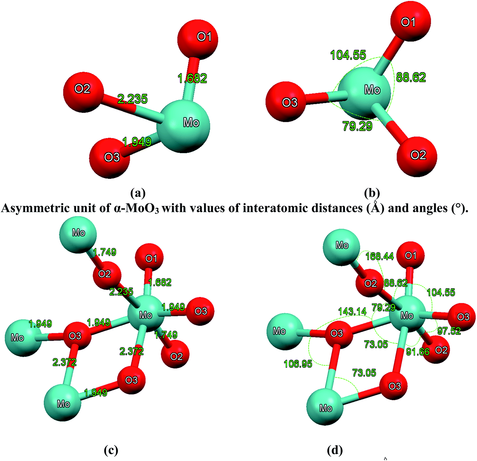 | ||
| Fig. 2 (a–b) Asymmetric unit of α-MoO3 with values of interatomic distances (Å) and angles (°); (c–d) octahedral MoO6 building unit with values of interatomic distances (Å) and angles (°). The octahedral MoO6 contains metal–oxygen bonds whose lengths vary between 1.68 Å and 2.37 Å. The O1 atom is coordinated to one Mo atom with distance of about 1.68 Å, which is in good agreement with the experimental value of 1.67 Å;28–30 the asymmetric bridging oxygen O2 are situated asymmetrically between two Mo with distances of 1.74 and 2.23 Å, respectively, in good agreement with the experimental values of 1.73 and 2.25 Å.28–30 The symmetric bridging O3 is located symmetrically between two Mo atoms with a distance of about 1.94 Å and linked to another Mo atom with a distance of about 2.37 Å, which is in good agreement with the experimental values of 1.94 and 2.33 Å.28–30 | ||
 | ||
| Fig. 3 The calculated electronic band structure of α-MoO3 using LDA, GGA, EVGGA and mBJ. | ||
To comprehensively understand the electronic structures, the total density of states of α-MoO3 was determined using LDA, GGA, EVGGA and mBJ, as illustrated in Fig. 4(a), which demonstrates the influences of replacing the exchange correlation potentials on the total density of states. This figure shows that replacing the exchange correlation potentials shifts the structures from CBM and above towards higher energies. This supports our previous finding that mBJ succeeds in bringing the calculated energy gap closer to the experimental one. Therefore, we present the partial density of states of α-MoO3 obtained by mBJ in Fig. 4(b–e). The energy region extending between −6.0 eV and Fermi level (EF) mainly originates from Mo-d and O1,2,3-p states with small contributions from Mo-s/p and O1,2,3-s states. It is clear that there exists a strong hybridization between Mo-d and O-p states and also between Mo-s/p and O-s states. The energy region from the CBM and above is mainly formed by Mo-d and O1,2,3-p states with small contributions from Mo-s/p and O1,2,3-s states. The CBM is mainly formed by Mo-d state whereas the VBM is a mixture of O1,2,3-p states. The energy region from CBM and above represents a weak hybridization between the states.
 | ||
| Fig. 4 (a) Calculated total density of states (states per eV per unit cell) using LDA, GGA, EVGGA and mBJ; (b) calculated Mo–s/p partial density of states (states per eV per unit cell) using mBJ; (c) calculated Mo-d partial density of states (states per eV per unit cell) using mBJ; (d) calculated O1,2,3-s partial density of states (states per eV per unit cell) using mBJ; (e) calculated O1,2,3-p partial density of states (states per eV per unit cell) using mBJ. | ||
The electronic space charge density distribution of α-MoO3 is explored to study the origin of chemical bonds between the atoms. The two crystallographic planes, namely (0 0 1) and (1 0 1), are represented in Fig. 5(a) and (b), respectively. It is found that the majority of charges are accumulated on the O site and the distribution of electronic charge is spherical, which results in the bonding between Mo–O showing prevailingly ionic and partially covalent features due to the large electro-negativity difference between Mo (2.16) and O (3.44). The two crystallographic planes confirm that the valence electrons from the Mo site are transferred to the O site. This can be seen easily by color charge density scale, where blue color (+1.000) corresponds to the maximum charge accumulation site. From the electro-negativity difference one can determine the degree of covalency, which is a very important factor to estimate the hardness of materials.27
 | ||
| Fig. 5 The calculated electron charge density distribution were calculated in two crystallographic planes; (a) (0 0 1) crystallographic plane of α-MoO3; (b) (1 0 1) crystallographic plane of α-MoO3. Because the crystallographic planes (0 0 1) and (1 0 1) do not show all the details, please refer to Fig. 2 and its caption. | ||
The interatomic distances (see Fig. 2(a) and c) represent the anisotropic nature of bonds in α-MoO3 which is confirmed by the two crystallographic planes (0 0 1) and (1 0 1). The O1 atom is coordinated to one Mo atom with a distance of about 1.68 Å, which is in good agreement with the experimental value of 1.67 Å;28–30 the asymmetric bridging oxygens O2 are situated asymmetrically between two Mo with distances of 1.74 and 2.23 Å, respectively, in good agreement with the experimental values of 1.73 and 2.25 Å.28–30 The symmetric bridging O3 is located symmetrically between two Mo atoms with a distance of about 1.94 Å and linked to another Mo atom with a distance of about 2.37 Å, in good agreement with the experimental values of 1.94 and 2.33 Å.28–30 The calculated bond distances in comparison with the experimental data28–30 are listed in Table 2 and illustrated in Fig. 2(a) and (c). In addition, we have calculated the bonds angles as represented in Fig. 2(b) and (d).
3.2. Effective mass
The effective masses and effective mass ratios of α-MoO3 compounds can be obtained from the curvature of the valence bands maximum (for the holes) and the conduction band minimum (for the electrons). The effective masses can be obtained through a simple parabolic fitting using the definition of effective mass as a second derivative of energy band with respect to the wave vector, k:
 | (1) |
The calculated electron effective mass ratio (m*e/me), heavy holes (m*hh/me) and light holes (m*lh/me) effective masses ratio of α-MoO3 compounds using mBJ are 0.0194, 0.0984 and 0.1034, respectively. It can be assumed that an electron in a solid moves as if it was a free electron but with an effective mass m* rather than a free electron mass. The larger the band curvature, the smaller the effective mass. It is quite clear from Fig. 3 that the valence bands are less dispersive in all the high symmetry directions. This would imply larger effective mass for the carriers belonging to these bands and hence low mobility μe = eτe/m*e and μh = eτh/m*h.31 However, presence of carriers with large mobility is required for obtaining a higher electrical conductivity (σ = ne(μe + μh)). The electron mobility characterizes how quickly an electron can move through a metal or semiconductor.
3.3. Linear optical response
To obtain the imaginary part of the optical dielectric function's dispersion for the orthorhombic α-MoO3, we need to calculate three tensor components along the polarization directions [1 0 0], [0 1 0] and [0 0 1] with respect to the crystalline axes. These are εxx(ω), εyy(ω) and εzz(ω), which can be evaluated using a formula found in the literature.32,33 Fig. 6(a) exhibits the imaginary part of the optical dielectric function's dispersion. Broadening is taken to be 0.1 eV, which is typical of the experimental accuracy. The threshold for the optical transitions (optical absorption's edge) between the top of valence band and bottom of conduction band occurs at around 2.81 eV. The ε2xx(ω), ε2yy(ω) and ε2zz(ω) components display two principle peaks, the highest one is situated around 5.0 eV and the second one is situated around 8.5 eV. The first structure occurs due to the optical transitions between Mo-s/p and O1,2,3-s/p states. The second structure is formed due to the electric-dipole transitions between Mo-s/p and O1,2,3-s/p of the VBs to Mo-p and O1,2,3-p of the CB. It is interesting to highlight that there is a considerable anisotropy between ε2xx(ω), ε2yy(ω) and ε2zz(ω) tensor components of the frequency dependent dielectric function. Fig. 6(a) shows that there are two absorption regions, a high absorption region occurs between 2.81 and 6.5 eV and a low absorption region occurs between 8.0 eV and 10.0 eV, where the materials exhibit high transparency. The regions confined between 6.5 and 8.0 eV and 10.0 and 13.5 eV are considered as lossless regions.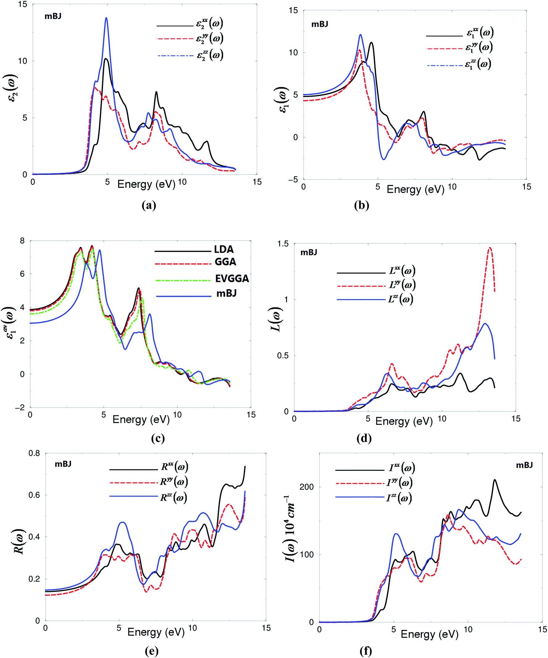 | ||
| Fig. 6 (a) Calculated ε2xx(ω) (dark solid curve-black color online), ε2yy(ω) (light dashed curve-red color online) and ε2zz(ω) (light solid curve-blue color online); (b) calculated ε1xx(ω) (dark solid curve-black color online); ε1yy(ω) (light dashed curve-red color online) and ε1zz(ω) (light solid curve-blue color online); (c) calculated εLDA1(ω) (dark solid curve-black color online); εGGA1(ω) (light dashed curve-red color online); εEVGGA1(ω) (light dotted dashed curve-green color online); εmBJ1(ω) (light solid curve-blue color online); (d) calculated Lxx(ω) (dark solid curve-black color online), Lyy(ω) (light dashed curve-red color online) and Lzz(ω) (light solid curve-blue color online); (e) calculated Rxx(ω) (dark solid curve-black color online), Ryy(ω) (light dashed curve-red color online) and Rzz(ω) (light solid curve-blue color online); (f) calculated Ixx(ω) (dark solid curve-black color online), Iyy(ω) (light dashed curve-red color online) and Izz(ω) (light solid curve-blue color online). | ||
The real parts ε1xx(ω), ε1yy(ω) and ε1zz(ω) of the frequency dependent dielectric function can be obtained with the aid of Kramers–Kronig relations33 and the existence information about the imaginary parts ε2xx(ω), ε2yy(ω) and ε2zz(ω) of the optical dielectric functions. Fig. 6(b) illustrates the real part that again shows the existence of the anisotropy between the three tensor components.
The calculated values of ε1xx(0), ε1yy(0) and ε1zz(0) using mBJ are 4.80, 4.32 and 5.03, respectively. We should emphasize that ε1(0) corresponds to the optical dielectric constant, also known as ε∞. This corresponds only to the electron contribution to the total dielectric constant. The uniaxial anisotropy δε = [(εII0 − ε⊥0)/εtot0] = 0.154, indicating the existence of considerable anisotropy between the parallel (εII2(0) = ε1zz(0)) and the perpendicular 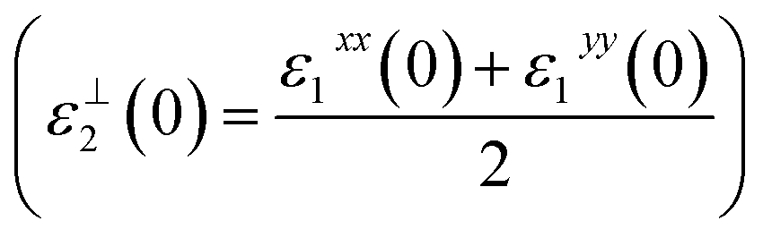 polarization directions. The calculated values of ε1xx(0), ε1yy(0), ε1zz(0) and εav1(0) within LDA, GGA and EVGGA are presented in the ESI.† We would like to demonstrate the influence of the exchange correlation potential on the value of the energy gap and hence on the optical properties. Therefore, we plot the average of the real parts εav1(ω) obtained from LDA, GGA, EVGGA and mBJ in Fig. 6(c), which shows that mBJ gives the lowest values. We note that a smaller energy gap yields a larger ε1(0) value. This could be explained on the basis of the Penn's model.34 Penn proposed a relation between ε(0) and Eg, ε(0) ≈ 1 + (ℏωP/Eg)2. Eg is some kind of averaged energy gap that could be related to the real energy gap. It is clear that ε(0) is inversely proportional to Eg. Therefore, a larger Eg yields a smaller ε(0).35,36 This finding support our previous observation from the calculated electronic band structure and the density of states, which shows that LDA, GGA and EVGGA underestimate the energy band gap, while mBJ succeeded in bringing the calculated energy band gap closer to the experimental one.
The other optical properties, such as reflectivity spectra R(ω), absorption coefficient I(ω) and the electron loss function L(ω), can be evaluated with the aid of the existing information on the calculated imaginary and real parts of the frequency dependent dielectric function. Fig. 6(d) illustrates the loss function L(ω), which confirms the existence of the lossless regions 6.5–8.0 eV and 10.0–13.5 eV, which is in agreement with our observation in Fig. 6(a). The peaks of loss function represent the plasma frequencies (ωP). We should emphasize that above ωP, the material behaves as dielectric, where ε1(ω) is positive, while below ωP, where ε1(ω) is negative, the material exhibits a metallic nature.
Fig. 6(e) illustrates the optical reflectivity R(ω) as a function of photon energy. It is clear that at low energies α-MoO3 compound exhibits a low reflectivity of about 17.0%, which then gradually increases to reach 50%, forming the first reflectivity maximum at about 5.0 eV. The first reflectivity minima occurs between 6.5 and 8.0 eV confirming the occurrence of a collective plasmon resonance. The depth of the plasmon minimum is determined by the imaginary part of the frequency dependent optical dielectric function at the plasma resonance and is representative of the degree of overlap between the inter-band absorption regions. Fig. 6(f) represents the absorption coefficient I(ω) of α-MoO3; it shows that there are two absorption bands, the first one extends between 2.81 and 6.5 eV and the second one between 8.0 eV and 13.5 eV in which the crystal exhibits high transparency.
4. Conclusions
The electronic band structure, density of states, electronic charge density distribution, chemical bonding and the linear optical properties of the orthorhombic molybdenum trioxide α-MoO3 were calculated. We employed density functional theory based on an all-electron full potential linear augmented plane wave (FPLAPW) method as implemented in the WIEN2k code within four types of exchange correlation potentials. Calculation demonstrated that α-MoO3 is an indirect band gap insulator. The CBM is situated at Γ point of BZ, whereas the VBM is located at T point of BZ. The calculated electronic band structure and the total density of states confirmed that mBJ brings the calculated energy band gap (2.81 eV) closer to the experimental one (3.03 eV and 3.1 eV). The electronic space charge density distribution of α-MoO3 was explored in two crystallographic planes (0 0 1) and (1 0 1) to study the origin of the chemical bonds. It is found that the majority of the charges are accumulated on the O site and the distribution of electronic charge is spherical. The two crystallographic planes confirm that valence electrons from the Mo site are transferred to O site.The interatomic distances represent the anisotropic nature of the bonds in α-MoO3, which is confirmed by the two crystallographic planes (0 0 1) and (1 0 1). The calculated bond distance is in very good agreements with the experimental data. The optical properties are calculated for three tensor components along the polarization directions [1 0 0], [0 1 0] and [0 0 1] with respect to the crystalline axes. It is found that the regions confined between 6.5 and 8.0 eV and 10.0 and 13.5 eV are considered as lossless regions. The calculated optical properties support our previous observation from the calculated electronic band structure and the density of states, which showed that LDA, GGA and EVGGA underestimate the energy band gap, while mBJ succeeded in bringing the calculated energy band gap closer to the experimental one.
Associated content
Full information about the calculated electronic band structures of α-MoO3 using; (a) LDA; (b) GGA; (c) EVGGA; (d) mBJ. The calculated energy band gaps in comparison with the experimental value. The calculated ε1xx(0), ε1yy(0), ε1zz(0) and εav1(0) of α-MoO3 using; (a) LDA; (b) GGA; (c) EVGGA; (d) mBJ.Acknowledgements
The result was developed within the CENTEM project, reg. no. CZ.1.05/2.1.00/03.0088, cofunded by the ERDF as part of the Ministry of Education, Youth and Sports OP RDI programme and, in the follow-up sustainability stage, supported through CENTEM PLUS (LO1402) by financial means from the Ministry of Education, Youth and Sports under the “National Sustainability Programme I”. Computational resources were provided by MetaCentrum (LM2010005) and CERIT-SC (CZ.1.05/3.2.00/08.0144) infrastructures.References
- G. Eranna, B. C. Joshi, D. P. Runthala and R. P. Gupta, Crit. Rev. Solid State Mater. Sci., 2004, 29, 111–188 CrossRef CAS.
- D. Lee, D.-j. Seong, I. Jo, F. Xiang, R. Dong, S. Oh and H. Hwang, Appl. Phys. Lett., 2007, 90, 122104 CrossRef.
- C.-S. Hsu, C.-C. Chan, H.-T. Huang, C.-H. Peng and W.-C. Hsu, Thin Solid Films, 2008, 516, 4839–4844 CrossRef CAS.
- F. Wang and W. Ueda, Chem.–Eur. J., 2009, 15(3), 742–753 CrossRef CAS PubMed.
- J. S. Chen, Y. L. Cheah, S. Madhavi and X. W. Lou, J. Phys. Chem. C, 2010, 114, 8675–8678 CAS.
- M. C. Rao, K. Ravindranadh, A. Kasturi and M. S. Shekhawat, Res. J. Recent Sci., 2013, 2(4), 67–73 Search PubMed.
- A. Klinbumrung, T. Thongtem and S. Thongtem, J. Nanomater., 2012, 930763 Search PubMed.
- L. Kihlborg, Ark. Kemi, 1963, 21, 357–364 CAS.
- H. Negishi, S. Negishi, Y. Kuroiwa, N. Sato and S. Aoyagi, Phys. Rev. B: Condens. Matter Mater. Phys., 2004, 69, 064111 CrossRef.
- J. B. Parise, E. M. McCarron III, R. V. Von Dreele and J. A. Goldstone, Solid State Chem., 1991, 93, 193–201 CrossRef CAS.
- E. M. McCarron III and J. C. Calabrese, Solid State Chem., 1991, 91, 121–125 CrossRef.
- C. V. Ramana, I. B. Troitskaia, V. V. Atuchin, M. Ramos and D. Ferrer, J. Vac. Sci. Technol., A, 2010, 28, 726–729 CAS.
- H.-J. Lunk, H. Hartl, M. A. Hartl, M. J. G. Fait, I. G. Shenderovich, M. Feist, T. A. Frisk, L. L. Daemen, D. Mauder, R. Eckelt and A. A. Gurinov, Inorg. Chem., 2010, 49(20), 9400–9408 CrossRef CAS PubMed.
- V. V. Atuchin, T. A. Gavrilova, T. I. Grigorieva, N. V. Kuratieva, K. A. Okotrub, N. V. Pervukhina and N. V. Surovtsev, J. Cryst. Growth, 2011, 318, 987–990 CrossRef CAS.
- A. H. Reshak and S. Auluck, RSC Adv., 2014, 4, 37411 RSC.
- A. H. Reshak, RSC Adv., 2014, 4, 39565 RSC.
- M. Jamal, N. Kamali Sarvestani, A. Yazdani and A. H. Reshak, RSC Adv., 2014, 4, 57903 RSC.
- A. H. Reshak, RSC Adv., 2014, 4, 63137 RSC.
- C. Diaz, V. Lavayen and C. Dwyer, J. Solid State Chem., 2010, 183, 1595–1603 CrossRef CAS.
- P. Blaha, K. Schwarz, G. K. H. Madsen, D. Kvasnicka and J. Luitz, WIEN2k, An augmented plane wave plus local orbitals program for calculating crystal properties, Vienna University of Technology, Austria, 2001 Search PubMed.
- J. P. Perdew, S. Burke and M. Ernzerhof, Phys. Rev. Lett., 1996, 77, 3865 CrossRef CAS PubMed.
- W. Kohn and L. J. Sham, Phys. Rev. A, 1965, 140, 1133 CrossRef.
- E. Engel and S. H. Vosko, Phys. Rev. B: Condens. Matter Mater. Phys., 1993, 47, 13164 CrossRef CAS.
- F. Tran and P. Blaha, Phys. Rev. Lett., 2009, 102, 226401 CrossRef PubMed.
- R. S. Patil, M. D. Uplane and P. S. Patil, Int. J. Electrochem. Sci., 2008, 3, 259–265 CAS.
- V. Shrotriya, G. Li, Y. Yao, C. W. Chu and Y. Yang, Appl. Phys. Lett., 2006, 88(1–6), 073508 CrossRef.
- F. M. Gao, J. L. He, E. Wu, S. M. Liu, D. L. Yu, D. C. Li, S. Y. Zhang and Y. J. Tian, Phys. Rev. Lett., 2003, 91, 015502 CrossRef PubMed Further modification has been made to the microscopic model of hardness by taking into account the effects of metallicity on the hardness.
- R. Tokarz-Sobieraj, K. Hermann, M. Witko, A. Blume, G. Mestl and R. Schlogl, Surf. Sci., 2001, 489, 107–125 CrossRef CAS.
- M. C. Rao, K. Ravindranadh, A. Kasturi and M. S. Shekhawat, Res. J. Recent Sci., 2013, 2(4), 67–73 Search PubMed.
- L. A. Kihlborg, Refinement of the crystal structure of Molybdenum trioxide, Ark. Kemi, 1963, 21, 471 CAS.
- W. Shi, J. Chen, J. Xi, D. Wang and Z. Shuai, Chem. Mater., 2014, 26, 2669 CrossRef CAS.
- F. Bassani and G. P. Parravicini, Electronic States and Optical Transitions In Solids, Pergamon Press Ltd., Oxford, 1975, pp. 149–154 Search PubMed.
- F. Wooten, Optical properties of solids, Academic press, New York and London, 1972 Search PubMed.
- D. R. Penn, Phys. Rev. B: Solid State, 1962, 128, 2093 CAS.
- T. Le Bahers, M. Rérat and P. Sautet, J. Phys. Chem. C, 2014, 118, 5997 Search PubMed.
- M. Gajdoš, K. Hummer, G. Kresse, J. Furthmüller and F. Bechstedt, Phys. Rev. B: Condens. Matter Mater. Phys., 2006, 73, 045112 CrossRef.
Footnote |
| † Electronic supplementary information (ESI) available. See DOI: 10.1039/c5ra00081e |
| This journal is © The Royal Society of Chemistry 2015 |