Comparative supercapacitance performance of CuO nanostructures for energy storage device applications†
V. Senthilkumara,
Yong Soo Kim*a,
S. Chandrasekaranb,
Balasubramaniyan Rajagopalanb,
Eui Jung Kimb and
Jin Suk Chungb
aDepartment of Physics and Energy Harvest Storage Research Center (EHSRC), University of Ulsan, Ulsan 680-749, South Korea. E-mail: yskim2@ulsan.ac.kr
bSchool of Chemical Engineering, University of Ulsan, Ulsan 680-749, South Korea
First published on 9th February 2015
Abstract
In the present study, three different morphologies of copper oxide (CuO) nanostructures; bud-, flower- and plate-shaped CuO structures were synthesized by a simple chemical method. Binder-included pseudocapacitor electrodes were prepared using bud- and flower-shaped CuO structures whereas, directly grown CuO-nanoplates on Ni foam were used as a binder-free electrode in a three-electrode setup for electrochemical studies. Remarkably, the binder-free CuO nanoplates electrode exhibited excellent specific capacitance of 536 F g−1 at a current density of 2 A g−1, whereas the binder-included electrodes of bud- and flower-shaped CuO exhibited 230 F g−1 and 296 F g−1, respectively, at a current density of 0.7 A g−1 in a 6 M KOH electrolyte. The cycling retention test and charge/discharge stability for the binder-free CuO nanoplates electrode showed 94% capacity retention after 2000 cycles and capacitance loss of only 11.3% over ∼1000 cycles at a current density of 4 A g−1 from charge/discharge measurements. Also, the binder-free CuO electrode showed higher energy and power densities of 29.4 W h kg−1 and 12.7 W kg−1, respectively, at 1.96 A g−1 in an asymmetrical device, when compared to the binder-included electrode of flower-shaped CuO.
1. Introduction
Due to the increasing demand for fossil fuels and the issue of global warming, electrochemical energy storage devices such as fuel cells, batteries and supercapacitors are required for the development of clean energy technology.1,2 The batteries used over recent decades have a low power density (i.e. slow charge/discharge rates) and a high energy density; while in contrast, conventional dielectric capacitors possess a high power density but lack a large energy density. Hence, it is now a necessity to develop systems which can simultaneously provide high energy density as well as high power density.3In recent years, electrochemical supercapacitors have gained significant research interest due to their high power density, reversibility and long cycle life.4,5 The supercapacitors are broadly classified based on their storage mechanism as electrical double layer capacitors (EDLCs) or pseudocapacitors. The non-Faradaic reaction with the accumulation of charge through electrostatic interactions at the electrode/electrode interface forms the basis of the energy storage mechanism of EDLCs, while that of pseudocapacitors is due to the fast Faradaic redox reaction on the surface of electro-active materials.6,7 To date, the widely used electrodes in EDLCs are carbon based materials, due to their good processing ability, large surface area/porosity, good cycle life, and low cost,8,9 but the devices so fabricated suffer from a relatively lower capacity in storing charge.
In contrast, the electrochemical pseudocapacitors have been shown to possess higher electrical conductivity and faster cation dispersion, thus resulting in much higher power densities and energy densities.10–14 Transition metal oxides having a rich redox reaction are a class of ideal supercapacitor electrode materials that have drawn intense interest recently, among other materials.15,16 Previously, hydrous ruthenium oxides (RuO) were used as electrode materials. However, the high cost of these materials limits their application in large scale manufacturing. Hence, efforts have been focused on the search for alternative and cheaper electrode materials including NiO,17 Co3O4 (ref. 18) and MnO2 (ref. 19) to explore their potential for the construction of supercapacitors with enhanced energy and power densities. Among these metal oxides, CuO is a promising candidate due to its cost effectiveness, abundance, eco-friendly nature, and the existence of simple methods for the preparation of various nanosized CuO structures. Its application as an electrode material for rechargeable Li-ion batteries20 showed remarkably high Li-ion storage capacities, through a redox reaction. Recently, a few works have investigated CuO for pseudocapacitor electrode applications.21–23 However, compared to the other metal oxides, the reported capacitance values for CuO electrodes are still low (<32%) though it has a high theoretical capacitance value of around 1783 F g−1 within the window of 0.68 V.24
Herein, we report a facile, cost-effective and scalable synthesis approach to prepare three different morphologies of CuO nanostructures; bud-, flower- and plate-shaped CuO structures, by a simple chemical method. The morphological, structural and electrochemical properties of the obtained CuO nanostructures were investigated. The bud- and flower-shaped CuO structures were prepared in powder form by a simple hydrothermal method and these powders were used for electrode preparation with the help of a binder (PVDF), whereas binder-free seed mediated CuO nanoplates grown on Ni foam were directly used as an electrode for the electrochemical studies. Remarkably, the seed mediated growth binder-free CuO nanoplates electrode exhibited a promising specific capacitance and excellent capacitance retention during cycling tests.
2. Experimental
2.1 Synthesis of bud and flower-shaped CuO nanostructures
Copper oxide nanostructures were synthesized as suggested by Pike et al.25 with slight modifications. In brief, aqueous solutions of copper nitrate (Cu(NO3)2·3H2O) and hexamethylenetetramine (HMT) (C6H12N4) were mixed separately with deionized water to an equal molar concentration of 0.02 M. The solutions were stirred separately for 30 min and then mixed uniformly. The mixture was kept at 120 °C for either 6 or 18 hours of reaction time. The precipitated product thus formed was collected and washed with methanol several times to remove the ionic impurities. Finally, the collected powders were annealed at 400 °C for an hour and the obtained powder was used for further analysis and capacitance studies.2.2 Seed mediated growth of copper oxide nanoplates on Ni foam
Synthesis of CuO nanoplates on Ni foam (density: 320 g m−2, pore size: 680 μm, thickness: 1.7 mm, Hittite Co., Ltd, S. Korea) was carried out by using a CuO nanoseed-mediated growth method. In a typical process, CuO nanoseed particles were first grown on Ni foam via an alcohothermal method. After a standard cleaning process, Ni foam was immersed in a 25 mM ethanolic solution of copper(II) acetate (Cu(CO2CH3)2) at 60 °C for 45 min. The Ni foam was then air-dried and annealed at 250 °C for 30 min to obtain a CuO nanoseed layer. Next, to form the CuO nanoplates, the above substrate was vertically dipped in an equimolar solution (13 mM) of copper nitrate trihydrate and HMT in deionized (DI) water at 120 °C for 16 hours. The substrate was then taken out of the growth solution and a homogeneous red brown layer was observed over the surface of Ni foam. Finally, the samples were rinsed with DI water gently several times and annealed at 400 °C for an hour in air. The weight of the deposited CuO was accurately calculated from the difference in the weight of the substrate before the chemical bath process and with CuO loading after calcinations using an analytical micro balance. The weight was found to be 2.4 mg cm−2.The prepared final CuO products were analyzed with various characterization tools. The structural and morphological studies were done by X-ray diffraction (Rigaku-X-ray diffractometer with Cu Kα radiation), and field emission-scanning electron microscopy (JEOL JSM 6500F) analysis. The optical and chemical composition was investigated using Raman (Thermo Scientific DXR Raman spectrophotometer) and X-ray photoelectron spectroscopy (XPS, Theta Probe AR-XPS System, Thermo Fisher Scientific) analysis. The surface area and porosity of the sample was confirmed using Brunauer–Emmett–Teller (BET-micromeritics ASAP 2020) measurements.
2.3 Electrochemical measurements
The electrochemical measurements were performed using a computerized potentiostat (IvimStat, IVIUM Tech.) under ambient conditions. A typical electrochemical measurement with a three-electrode cell system was employed, which was composed of CuO as the working electrode, a platinum plate as the counter electrode, and an Ag/AgCl as the reference electrode. In the case of CuO powder, the working electrode was fabricated by mixing 80 wt% as-prepared CuO with 10 wt% carbon black and 10 wt% polyvinylidene fluoride (PVDF), and slurry of the above mixture was painted onto a clean Cu foil (1 cm × 1 cm) to act as the current collector. The loading mass of each of the binder-included CuO electrodes was around 0.6 mg cm−2. The coated film was then dried in a vacuum cabinet at 80 °C, kept overnight to remove the excess solvent and water. Whereas, the CuO film on Ni foam (1 cm × 1 cm) was directly used as the working electrode.3. Results and discussion
3.1 Characterizations and growth process of CuO nanostructures
FE-SEM images and the corresponding energy-dispersive X-ray (EDX) spectra of the hydrothermally grown CuO nanostructures in two time intervals are shown in Fig. 1(a–c) and (e–g), respectively. The images show that the reaction time clearly influences the morphological changes of CuO. Bud-shaped CuO (Cu/CuO-1) nanostructures were obtained when the hydrothermal reaction proceeded for 6 h and the typical SEM images at different magnifications are shown in Fig. 1(a–c). On extending the reaction time to 18 h, flower-shaped CuO (Cu/CuO-2) was obtained as shown in Fig. 1(e–g). The size of the flowers was approximately in the range of 10–15 μm. A view of a single flower-shaped structure is shown in Fig. 1(g), it clearly reveals that the flowers consist of many triangular-shaped petals. The diameter of the petals varied from the base to the tip, i.e. sharpened tips with wider bases. The wider base of the petals connected to each other, rooted in the center to form a beautiful flower-like morphology. Fig. 1(i–k) show SEM images of the CuO nanoplates (Ni/CuO) grown uniformly on the nickel foam and the SEM image at lower magnification shows the CuO to form a uniform film all over the substrate. The SEM image at higher magnification indicates the majority of the nanoplates to be orientated almost vertically to the nickel foam substrate. The thickness of a single nanoplate was up to around 20 nm. EDX spectra (Fig. 1(d), (h) and (l)) clearly demonstrated the presence of Cu and O peaks and quantitative analysis revealed that the Cu and O were almost in a stoichiometrically equivalent ratio for all the CuO nanostructures.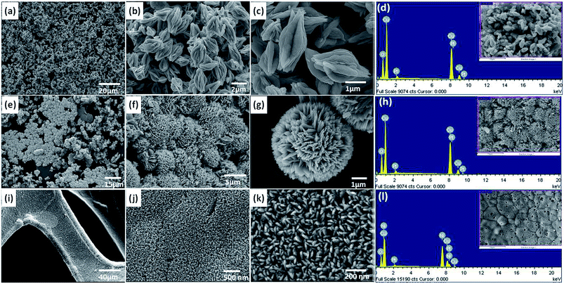 | ||
| Fig. 1 FE-SEM images of the CuO at low and high magnification and corresponding EDX images. (a–d) 6 h (bud shaped-CuO), (e–h) 18 h (flower shaped-CuO) and (i–l) CuO nanoplates on Ni foam. | ||
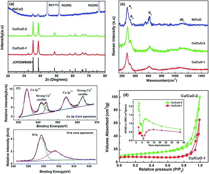
XRD analysis was used to investigate the structure of the synthesized samples. Fig. 2(a) depicts typical XRD patterns of the samples synthesized through the hydrothermal method and CuO-nameplates directly grown on Ni foam. In the XRD patterns, when compared with the standard diffraction peaks from JCPDS card no. 5-0661, the peaks located at 2θ values of 20–80° were indexed to the characteristic diffractions of monoclinic phase CuO. The peak intensities and width clearly indicated the sample to be highly crystalline in nature. The absence of other characteristic peaks, which could belong to impurities such as Cu(OH)2 or Cu2O, indicated that the obtained product was phase-pure. Therefore, it was obvious that the sample was composed of pure monoclinic phase CuO, which is consistent with the EDX analysis.
Raman spectroscopy, which is a sensitive probe of the local atomic arrangements and vibrations of materials, has been widely used to investigate the microstructural nature of nanosized materials.26 Fig. 2(b) shows the Raman spectra of the Cu/CuO-1 and Cu/CuO-2 morphologies. It shows the presence of three Raman peaks at 289.3, 338.5 and 622.7 cm−1, with the second one being the weakest and the third being broad. In comparison with the vibrational spectrum of a single CuO crystal,27 the peak at 289.3 cm−1 can be assigned to the Ag mode, whereas the peaks at 338.5 and 622.7 cm−1 can be assigned to the Bg modes, which is comparable to the reported data for nanocrystal CuO.28 In addition, a broadened peak at 1120 cm−1 was observed, which can be assigned to the multi-phonon (MP) transition of the CuO nanostructures.27 Therefore, from the Raman analysis it was evident that the synthesized product consists of single-phase CuO with a monoclinic structure.
To further confirm the elemental composition of the prepared CuO nanostructures, XPS analysis was used to determine the oxidation state of the Cu. All the binding energies obtained in the XPS analysis were calibrated using the C 1s signal at 284.5 eV as a reference to correct any electrical charging effect of the sample surface. Fig. 2(c) shows the Cu 2p and O 1s core-level spectra of the Cu/CuO-2 sample. The Cu 2p core-level spectrum represents two peaks located at 934.3 and 954.3 eV which correspond to Cu 2p3/2 and Cu 2p1/2, respectively. These values correspond with the data reported for the Cu 2p in CuO.29–31 Also, the width of approximately 20 eV between these two Cu peaks is the same as in the standard spectrum of Cu. In addition to the Cu 2p3/2 and 2p1/2 peaks, typical CuO-satellite peaks appear at binding energies with intense shake-up satellite peaks at 941.7 and 944.2 eV, these two peaks are overlapping, and the existence of a strong satellite pattern at 962.6 for the Cu 2p rules out the possibility of the presence of the Cu2O phase.32,33 Since the 3d shell is expected to be completely filled in Cu2O, the shakeup satellite peaks indicate the presence of an unfilled Cu 3d9 shell, i.e., the existence of CuO at the surface.29,30,34 From the O 1s core level spectrum, the low binding energy peak at 529.5 eV is due to the oxygen in the CuO crystal lattice, which corresponds to the O–Cu bond, whereas the higher binding energy peak at 531.5 eV is due to the different chemical states of oxygen, such as surface hydroxide due to adsorbed water from the atmosphere.35 Thus, the XRD, Raman and XPS results support the fact that the nanostructures are composed mainly of CuO.
The specific surface areas and the porous nature of the powder samples are determined by measuring nitrogen adsorption–desorption isotherms as presented in Fig. 1(d), with the inset showing their corresponding pore size distribution (BJH). By comparing the isotherms and pore size distributions, it can be seen that the isotherm of the Cu/CuO-2 shows a wide hysteresis loop at a relative pressure range of 0.7–1.0 P/P0 and the corresponding BET specific surface area is calculated to be ∼30.6 m2 g−1 which is larger than the specific surface area (about 24.9 m2 g−1) of the Cu/CuO-1 structure. In addition, the mesopore size distributions based on the BJH method of both samples are further confirmed by the corresponding pore size distribution curves (inset in Fig. 1(d)). The high surface area and mesoporous structure of the Cu/CuO-2, when compared to Cu/CuO-1, provides an opportunity for the efficient diffusion and transportation of the electrolyte with the help of large pore channels, while the small pores provided more active sites for chemical reactions.36
3.2 Electrochemical analysis of CuO nanostructures
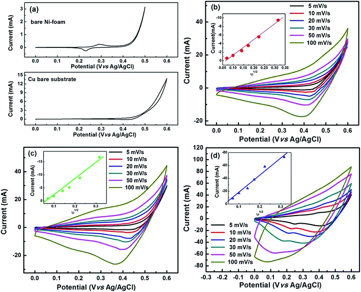
The electrochemical analyses for all the CuO electrodes were conducted in aqueous 6 M KOH solution. The merits of the use of alkali KOH electrolytes when compared to other organic electrolytes are their higher ionic concentration and lower resistance.12 Fig. 3(a) shows the CV curves of the bare Cu and nickel foam substrates at a voltage scan rate of 5 mV s−1. Both of the substrates exhibited CV curves with small areas, and anodic and cathodic peak currents of less than 300 μA. These results clearly suggest that the capacitance contribution from both of the substrates was minimal. Fig. 3(b–d) show the capacitance performance of the Cu/CuO-1, Cu/CuO-2 and Ni/CuO electrodes evaluated with cyclic voltammograms at different scan rates of 5, 10, 20, 30, 50 and 100 mV s−1 at room temperature. The current under the curve slowly increased with scan rate in all of the electrodes. This behavior clearly shows the voltammetric current to be directly proportional to the scan rates of CV, indicating an ideal capacitive behavior.37 When there is an increase of the scan rate, the anodic peaks shift towards the positive potential whereas the cathodic peaks shift towards the negative potential. This phenomenon demonstrates the quasi-reversible nature of the redox reaction. The plots of the cathodic peak current (ip) against ν1/2 (insets in Fig. 3(b–d)) show a nearly linear correlation, which suggests a diffusion-controlled electrode reaction with the electrolyte used.22The pseudocapacitance of transition metal oxides has been attributed to redox transitions of species at various oxidation states.38 Therefore, based on the present CV data and previously reported experimental results, the charging and discharging processes in the CuO electrode in alkaline (KOH) electrolyte at the potential range of 0–0.6 V can be summarized in the following reactions.24,39,40
 | (1) |
 | (2) |
| CuOH + OH− ⇔ CuO + H2O + e− | (3) |
| CuOH + OH− ⇔ Cu(OH)2 + e− | (4) |
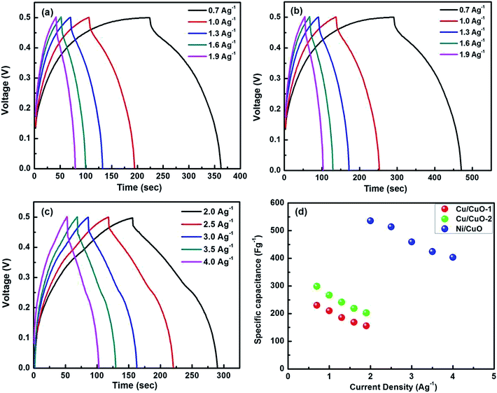
The capacitive performances of all the electrodes were evaluated with constant current charge/discharge measurements at different current densities as shown in Fig. 4(a–c). In order to avoid the occurrence of oxygen evolution, the electrode was charged and discharged within the potential range of 0–0.5 V vs. Ag/AgCl. The charge/discharge curves showed a good symmetry with nearly triangular shaped curves for all current densities, which demonstrated the good capacitive characteristics of the material even at high current density. The specific capacitance (Cs) of an electrode in a given electrolyte solution can be calculated using the following equation.21,22
 | (5) |
The excellent capacitance values of the Ni/CuO electrodes can be attributed to their structural features. The highly conductive nature of the 3D macroporous Ni foam enables efficient charge transport and accessible diffusion of electrolytes. Further, a good electrical contact between the current collector and the CuO nanoplates efficiently enhances more of the active material to contribute to the capacity i.e., the “dead volume” in the electrode is significantly reduced. Also, the interspaces between the adjacent nanoplates allows easy diffusion of the electrolyte into the nanoplate matrix to provide a large surface area for Faradaic reactions, which allows abundant adsorption of ions as well as enabling fast intercalation/de-intercalation of ions and charge transport. In addition, the thin layer of CuO nanoseeds may also contribute to the enhanced capacitive performance of the electrode.
The specific capacitance values of the binder-included electrodes of Cu/CuO-1 and Cu/CuO-2 were found to be 230 F g−1 and 296 F g−1, respectively, at a current density of 0.7 A g−1. The desirable high-rate capacitive behavior of the Cu/CuO-2 electrode is mainly attributed to the highly mesoporous structure of the electrode with a higher surface area (Fig. 2(d)) compared to Cu/CuO-1, which can significantly facilitate the penetration of protons or other cations into the whole electrode matrix.
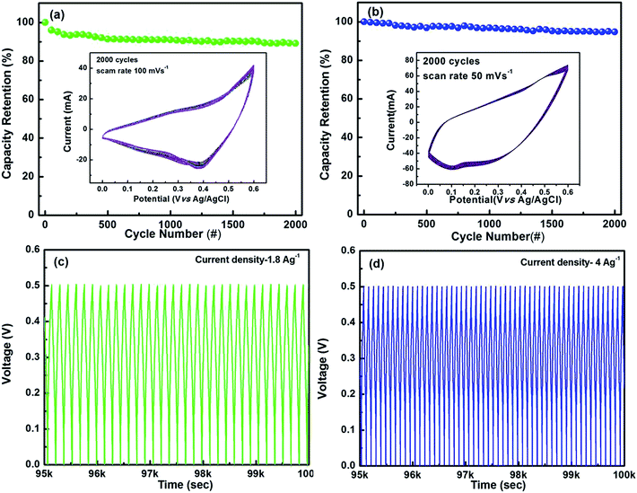
To investigate the stability of the Ni/CuO and Cu/CuO-2 electrodes, a cycling test was conducted over 2000 cycles as shown in Fig. 5. Fig. 5(b) shows the Ni/CuO exhibited little degradation even after the completion of 2000 repeated sweeps, thus confirming the good cycling stability of the electrode. Interestingly, 94% of the capacity was retained even after 2000 cycles as seen from Fig. 5(b). Thus, these results demonstrated the active electrode material i.e. Ni/CuO was very stable during the CV cycling test. Whereas, the binder-included Cu/CuO-2 electrode exhibited only 89% capacity retention after 2000 cycles (Fig. 5(a)). The capacitance loss is not only caused by the nature of the material itself but may also possibly be due to the continuous oxidation–reduction reactions, which in turn lead to a change in the volume of the active materials. This change thus results in an inefficient binding of the CuO with its PVDF matrix, thereby showing a reduction in the capacity retention.
The electrochemical stability was further confirmed for both electrodes by the charge/discharge measurements as shown in Fig. 5(c) and (d). The results showed an undistorted and essentially symmetric curve even after an extended period of charge and discharge cycles. The capacitance loss was found to be around 16% (∼650 cycles) for the Cu/CuO-2 electrode at the current density of 1.8 A g−1 while only 11.3% for the Ni/CuO electrode (∼1000 cycles) even at a higher current density of 4 A g−1. These results also showed that the Ni/CuO electrode presents a larger specific capacitance and excellent rate stability, which is a promising feature for the development of high-performance supercapacitors.
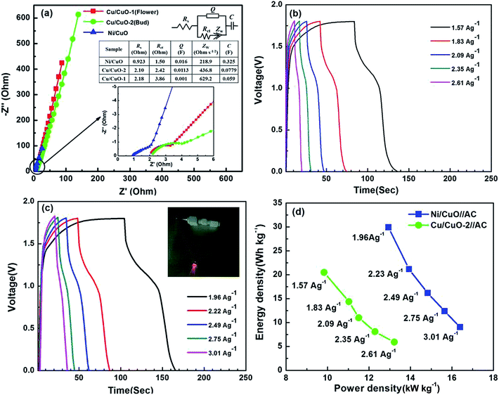
Electrochemical impedance spectroscopy (EIS) was carried out to understand the interfacial electronic properties of the Cu/CuO-1, Cu/CuO-2 and Ni/CuO electrodes in the frequency range of 100 kHz to 10 mHz at an open circuit potential by applying an AC voltage of 10 mV. The Nyquist plots showed capacitive behavior impedance spectra for all three electrodes (Fig. 6(a)). At higher frequency (Fig. 6(a) inset) the impedance spectra showed a distorted semicircle, followed by a linear shape in the lower frequency region. The equivalent circuit used for fitting the EIS spectra is as given in Fig. 6(a) and the electronic components as fitted by the solution resistance (Rs), charge transfer resistance (Rct), Warburg impedance (Zw), constant phase element (CPE) from the double layer and pseudo-Faradaic capacitance (C) are shown. Ni/CuO exhibits smaller Rs, demonstrating the good conductivity of the electrolyte and low internal resistance of the capacitor. The fitted results are presented as a table in Fig. 6(a). The Rct is also fairly low for the Ni/CuO (1.5 Ω) when compared to the binder-included electrodes, which indicates the improved ionic conduction and electrolyte diffusion to the CuO nanoplates on the Ni foam electrode.
The energy density (ED) and power density (PD) are the two most important parameters of electrochemical supercapacitor devices, which determine the operational performance/efficiency. To investigate the aforesaid properties of CuO nanostructures in a complete cell set up, symmetrical and asymmetrical devices were fabricated for the Cu/CuO-2 and Ni/CuO electrodes which showed a better capacitive performance in the three electrode system studies. The symmetrical device was composed of CuO nanostructures as the positive and negative electrodes, polypropylene as the separator and stainless steel as the current collectors (Fig. S1†). Whereas, activated carbon (AC) was used as the negative electrode along with CuO nanostructures as the positive electrode for the fabrication of asymmetrical devices. The CV curves, charge/discharge measurements and the capacitance values from the charge/discharge curves of the symmetric devices between 0 and 1.0 V in 6 M KOH electrolyte are shown in Fig. S2.† The cell maintained rectangular shaped CVs even at a higher scan rate of 150 mV s−1, indicating the ideal capacitive behavior and desirable fast charging/discharging property for power devices. Fig. 6(b) and (c) show the galvanostatic charge/discharge curves of the asymmetric devices at different current densities of both CuO nanostructures, which were used to evaluate the energy and power densities. The CVs and the capacitance values for the devices calculated from the charge/discharge curves are shown in Fig. S3.† The ED and PD values were calculated by using the following equations.41,42
 | (6) |
The Ragone plot for asymmetrical devices is shown in Fig. 6(d). The Ni/CuO electrode delivered a high energy density of about 29.4 W h kg−1 at a high power density of 12.7 kW kg−1. Further, the Ni/CuO electrode also showed a higher performance compared to the Cu/CuO-2 electrode in symmetric device studies (Fig. S2†). All these observations make the binder-free Ni/CuO nanoplates electrode a promising possible candidate for supercapacitor applications when compared to the binder-included electrodes of bud- and flower-shaped CuO nanostructures.
4. Conclusion
Three different morphologies of CuO electrodes, binder-free and binder-included, were prepared and investigated for their electrochemical properties. The results showed the binder-free CuO nanoplate electrode on Ni foam to exhibit higher utilization efficiency and better electrolyte diffusion compared to the binder-included electrodes of bud- and flower-shaped CuO. Excellent specific capacitance and stable cycling performance characteristics for a supercapacitor were exhibited by the synthesized Ni/CuO electrode. The cost-effective process, availability of the source materials, easy preparation method and better electrochemical properties make the Ni/CuO nanoplates an excellent source for electrode materials in the preparation of supercapacitors.Acknowledgements
This research was supported by the Basic Science Research Program (Grant no. 2014-010369), Priority Research Centers Program (Grant no. 2009-0093818), Leader Industry University Cooperation (LINC) project (Grant no. 2014E7268010115), and Basic Research Lab Program (Grant no. 2014R1A4A1071686) through the National Research Foundation of Korea (NRF) and funded by the Ministry of Education. The authors also thank Dr J.-S. Bae of Busan center, KBSI.References
- H.-C. Chien, W.-Y. Cheng, Y.-H. Wang and S.-Y. Lu, Adv. Funct. Mater., 2012, 22, 5038–5043 CrossRef CAS.
- A. S. Arico, P. Bruce, B. Scrosati, J.-M. Tarascon and W. van Schalkwijk, Nat. Mater., 2005, 4, 366–377 CrossRef CAS PubMed.
- X.-M. Liu, Z. d. Huang, S. w. Oh, B. Zhang, P.-C. Ma, M. M. F. Yuen and J.-K. Kim, Compos. Sci. Technol., 2012, 72, 121–144 CrossRef CAS PubMed.
- B. E. Conway, J. Electrochem. Soc., 1991, 138, 1539–1548 CrossRef CAS PubMed.
- R. Kötz and M. Carlen, Electrochim. Acta, 2000, 45, 2483–2498 CrossRef.
- E. Frackowiak and F. Béguin, Carbon, 2002, 40, 1775–1787 CrossRef CAS.
- W. Yong-gang and Z. Xiao-gang, Electrochim. Acta, 2004, 49, 1957–1962 CrossRef PubMed.
- K. Xie, X. Qin, X. Wang, Y. Wang, H. Tao, Q. Wu, L. Yang and Z. Hu, Adv. Mater., 2012, 24, 347–352 CrossRef CAS PubMed.
- X. He, R. Li, J. Qiu, K. Xie, P. Ling, M. Yu, X. Zhang and M. Zheng, Carbon, 2012, 50, 4911–4921 CrossRef CAS PubMed.
- L. Zhang and G. Shi, J. Phys. Chem. C, 2011, 115, 17206–17212 CAS.
- X. Zhao, B. M. Sanchez, P. J. Dobson and P. S. Grant, Nanoscale, 2011, 3, 839–855 RSC.
- G. Wang, L. Zhang and J. Zhang, Chem. Soc. Rev., 2012, 41, 797–828 RSC.
- C. Yuan, J. Li, L. Hou, X. Zhang, L. Shen and X. W. Lou, Adv. Funct. Mater., 2012, 22, 4592–4597 CrossRef CAS.
- J. Jiang, J. Liu, R. Ding, J. Zhu, Y. Li, A. Hu, X. Li and X. Huang, ACS Appl. Mater. Interfaces, 2010, 3, 99–103 Search PubMed.
- H. Jiang, T. Zhao, C. Yan, J. Ma and C. Li, Nanoscale, 2010, 2, 2195–2198 RSC.
- H. Jiang, T. Zhao, J. Ma, C. Yan and C. Li, Chem. Commun., 2011, 47, 1264–1266 RSC.
- K. R. Prasad and N. Miura, Appl. Phys. Lett., 2004, 85, 4199–4201 CrossRef CAS PubMed.
- V. Srinivasan and J. W. Weidner, J. Power Sources, 2002, 108, 15–20 CrossRef CAS.
- R. N. Reddy and R. G. Reddy, J. Power Sources, 2003, 124, 330–337 CrossRef CAS.
- H. Zhang, J. Feng and M. Zhang, Mater. Res. Bull., 2008, 43, 3221–3226 CrossRef CAS PubMed.
- G. Wang, J. Huang, S. Chen, Y. Gao and D. Cao, J. Power Sources, 2011, 196, 5756–5760 CrossRef CAS PubMed.
- Y.-K. Hsu, Y.-C. Chen and Y.-G. Lin, J. Electroanal. Chem., 2012, 673, 43–47 CrossRef CAS PubMed.
- L. Yu, Y. Jin, L. Li, J. Ma, G. Wang, B. Geng and X. Zhang, CrystEngComm, 2013, 15, 7657–7662 RSC.
- B. Vidhyadharan, I. I. Misnon, R. A. Aziz, K. P. Padmasree, M. M. Yusoffa and R. Jose, J. Mater. Chem. A, 2014, 2, 6578–6588 CAS.
- J. Pike, S.-W. Chan, F. Zhang, X. Wang and J. Hanson, Appl. Catal., A, 2006, 303, 273–277 CrossRef CAS PubMed.
- Y. Duan, J. F. Kong and W. Z. Shen, J. Raman Spectrosc., 2012, 43, 756–760 CrossRef CAS.
- J. C. Irwin, J. Chrzanowski, T. Wei, D. J. Lockwood and A. Wold, Phys. C, 1990, 166, 456–464 CrossRef CAS.
- J. F. Xu, W. Ji, Z. X. Shen, S. H. Tang, X. R. Ye, D. Z. Jia and X. Q. Xin, J. Solid State Chem., 1999, 147, 516–519 CrossRef CAS.
- Z. Ye, L. Hu, J. Jiang, J. Tang, X. Cao and H. Gu, Catal. Sci. Technol., 2012, 2, 1146–1149 CAS.
- Y. C. Zhang, J. Y. Tang, G. L. Wang, M. Zhang and X. Y. Hu, J. Cryst. Growth, 2006, 294, 278–282 CrossRef CAS PubMed.
- Z. Zhang and P. Wang, J. Mater. Chem., 2012, 22, 2456–2464 RSC.
- S. Poulston, P. M. Parlett, P. Stone and M. Bowker, Surf. Interface Anal., 1996, 24, 811–820 CrossRef CAS.
- J. F. Moulder, W. F. Stickle, P. E. Sobol and K. D. Bomben, Handbook of X-ray photoelectron spectroscopy, Perkin Elmer Eden Prairie, MN, 1992 Search PubMed.
- M. Yin, C.-K. Wu, Y. Lou, C. Burda, J. T. Koberstein, Y. Zhu and S. O’Brien, J. Am. Chem. Soc., 2005, 127, 9506–9511 CrossRef CAS PubMed.
- M. F. Al-Kuhaili, Vacuum, 2008, 82, 623–629 CrossRef CAS PubMed.
- S. K. Meher and G. R. Rao, Nanoscale, 2013, 5, 2089–2099 RSC.
- Y.-C. Chen, Y.-K. Hsu, Y.-G. Lin, Y.-K. Lin, Y.-Y. Horng, L.-C. Chen and K.-H. Chen, Electrochim. Acta, 2011, 56, 7124–7130 CrossRef CAS PubMed.
- N. Mukherjee, B. Show, S. K. Maji, U. Madhu, S. K. Bhar, B. C. Mitra, G. G. Khan and A. Mondal, Mater. Lett., 2011, 65, 3248–3250 CrossRef CAS PubMed.
- M.-J. Deng, C.-C. Wang, P.-J. Ho, C.-M. Lin, J.-M. Chen and K.-T. Lu, J. Mater. Chem. A, 2014, 2, 12857–12865 CAS.
- Y. X. Zhang, M. Huang, F. Li and Z. Q. Wen, Int. J. Electrochem. Sci., 2013, 8, 8645–8661 CAS.
- B. G. Choi, M. H. Yang, W. H. Hong, J. W. Choi and Y. S. Huh, ACS Nano, 2012, 6(5), 4020–4028 CrossRef CAS PubMed.
- J. Ji, L. L. Zhang, H. Ji, Y. Li, X. Zhao, X. Bai, X. Fan, F. Zhang and R. S. Ruoff, ACS Nano, 2013, 7(7), 6237–6243 CrossRef CAS PubMed.
Footnote |
| † Electronic supplementary information (ESI) available. See DOI: 10.1039/c5ra00035a |
| This journal is © The Royal Society of Chemistry 2015 |

