
Improved model for diffusion-limited current in organic metal-insulator-metal diodes
Muhammad Ammar Khana and
Sun Jiu-Xun*ab
aSchool of Physical Electronics, University of Electronic Science and Technology, Chengdu 610054, China. E-mail: sjx@uestc.edu.cn
bLaboratory for Shock Wave and Detonation Physics Research, Southwest Institute of Fluid Physics, Mianyang 621900, China
First published on 9th February 2015
Abstract
The analytic J–V formula for organic diodes recently derived by Bruyn et al. is improved by considering the electric field dependence of mobility. The improved formula is applied to four devices. The results calculated from the original formula cannot arrive at a good agreement with the experimental data. The results calculated from the improved analytic formula are in good agreement with the complete numerical solutions, and both agree with the experimental data very well.
1. Introduction
Because of the promise of low-cost and large-area electronic applications, organic semiconductors are the object of intense investigation.1–7 The current in metal-insulator-metal (MIM) organic diodes is space charge limited (SCL). It can be described by solving the Poisson and drift-diffusion equations simultaneously by using some formulae of mobility. These equations are difficult to analytically solve even taking mobility as a constant. So over long times, the SCL current was described by using the analytic Mott–Gurney formulae at high bias voltages with the diffusion current being negligible.But at low and middle voltages, the diffusion current cannot be neglected. And in many works the diffusion-limited current in organic MIM diodes has been analyzed using the classical Shockley diode equation,1 J = J0[exp(qV/ηkT) − 1]. Recently, Bruyn et al.2 pointed out that the Shockley equation was derived to describe a bipolar current through a p–n diode, where the ideality factor is strictly related to the order of recombination. Applying this equation to unipolar devices with undoped semiconductors is therefore questionable. They2 derived an analytical equation that describes the diffusion current for undoped semiconductors or insulators in MIM diodes with asymmetric contacts. This can substantially improve the accuracy of analysis of experimental data and charge-transport measurements in organic-semiconductor diodes. However, we notice that the mobility has been taken as constant in derivations of Bruyn et al.,2 so the resulting formulae is unsuitable for wide voltage ranges, and even for low and middle voltages the errors are non-negligible.
The traps have been recognized an important issue for SCL current characteristics to transport models.3–20 There are two types of models to consider trap effects in literature. The first type of models separate all carriers into free and trapped,3–10 two representative methods are the mobility edge (ME) model3–7 and trapped carrier model.8–10 The second type of models treats all carriers as mobile,11–18 the trap effects are considered by treating the mobility of carriers as a function of electric field or density of carriers. Two representative methods are the exponential model of Pai,11–14 and the unified model of Pasveer15 et al. The exponential model of Pai11 has ever been an empirical model. However, Dunlap et al.12 analytically derived the expression of mobility for organic semiconductors, confirmed the exponential model of Pai.11 Subsequently, Blom et al.14 proposed temperature dependent expressions for parameters in the exponential model. Pasveer et al.15 formulated the mobility as a function of temperature, density of charge carriers and electric field, and the model has been applied to many materials.15–18
In one of our recent work,19 we consider non-symmetric barriers at contacts in the models of Pai11 and Pasveer et al.15 and applied them to single-crystal rubrene organic semiconductor. Our results19 show that the exponential mobility model11–14 can well describe current–voltage (J–V) data of single-crystal rubrene, the extracted parameters show correct temperature dependence, and the extracted barriers are non-symmetric. However, the model of Pasveer et al.15 fails to fit J–V curves, and some parameters show inconsistent temperature dependence which should be constants in the theoretical framework of Pasveer et al. If comparing the model of Bruyn et al.2 with model in,11–14,19 it can be seen that the basic physical model of Bruyn et al.2 can be included in19 as special case. Since the exponential mobility model11–14,19 gives good description for typical diodes, and the analytic J–V formulae are very important and convenient for device modeling and analysis of experimental data, it is necessary to improve the analytic J–V formulae by using exponential mobility model.11–14,19
2. Outline of fundamental formulae
The Poisson equation for description of the SCL current is as follows3–19
 | (1) |
 | (2) |
![[thin space (1/6-em)]](https://www.rsc.org/images/entities/char_2009.gif) exp(−Wleft/kT), p(L) = Nfexp(−Wright/kT); φ(0) = Wleft + V, φ(L) = Wright; V − Vbi = φ(0) − φ(L). Bruyn et al.2 used different notations for potential barriers: φb = Wright, b = Wleft.
exp(−Wleft/kT), p(L) = Nfexp(−Wright/kT); φ(0) = Wleft + V, φ(L) = Wright; V − Vbi = φ(0) − φ(L). Bruyn et al.2 used different notations for potential barriers: φb = Wright, b = Wleft.
The numerical solutions of eqn (1)–(5) and eqn (6) are troublesome. In order to derive an analytic solution, Bruyn et al.2 proposed following analytic linear approximation for the Poisson eqn (1)
| φ(x) = V + b + (Vbi − V)(x/L) | (3) |
We notice that the electric field evaluated from eqn (3) is a constant being independent to coordinate
| F = −∂φ(x)/∂x = (V − Vbi)/L | (4) |
The exponential mobility model of Pai11 has been rationalized by Dunlap et al.12 and has following form
| μp(F) = μp(0)exp(γ√F) | (5) |
 | (6) |
As γ takes zero value, eqn (6) would reduce to the formula of Bruyn et al.2
Although the mechanism of electric conduction is not thoroughly determined, the Gaussian model3–19 for DOS has been recognized:  where N0, Ev, and σ are the total number of states, the center energy and the standard deviation of the Gaussian distribution, respectively. Assuming organic semiconductors are non-degenerate, the density of holes can be derived as,10,19 p = Nfexp[−qφ(x)/kT], with effective DOS defined as
|
Nf = N0exp[(Ev − EF)/kT]exp[σ2/2(kT)2]
| (7) |
The coefficient μp(0) in eqn (5) denotes the mobility at zero field. Blom et al.14 observed a thermally activated behavior
|
μp(0) = μ0exp(−Δ/kBT)
| (8) |
They also demonstrated the linear dependence between γ and 1/T, as following
 | (9) |
This empirical dependence of γ on T has originally been proposed by Gill.13
3. Results and discussions
We apply eqn (6) based on the modified exponential model11–14,19 to four different polymers: poly[4′-(3,7-dimethyloctyloxy)-1,1′-biphenylene-2,5-vinylene] (NRS-PPV),15 poly(2-methoxy-5-(3′,7′-dimethyloctyloxy)-p-phenylene vinylene) (OC1C10-PPV),15 poly(3-hexylthiophene) (P3HT),20 and poly(2-methoxy-5-(2-ethylhexyloxy)-1,4-phenylene-vinylene) (MEH-PPV),8,9 with their thickness of layer 560, 275, 95 and 270 nm, respectively. We calculate J–V curves from both analytic eqn (6) and numerical solutions of eqn (1) and (2). The theoretical results are compared with experimental data in Fig. 1. | ||
| Fig. 1 Comparison of calculated J–V curves by using modified model with experimental data6,8 for NRS-PPV, OC1C10-PPV,15 P3HT20 and MEH-PPV8,9 diodes with 560, 275, 95 and 270 nm thickness of organic layer at different temperatures. (solid lines: γ ≠ 0; dashed lines: γ = 0). | ||
The figure shows that the agreement of theoretical curves with experimental points is fairly good; covering all ranges of voltages involved and temperatures. However, the difference between results from analytic eqn (6) and numerical solutions of eqn (1) and (2) is very small and invisible in Fig. 1. Thus the analytic formula eqn (6) is a good approximation to numerical solutions of eqn (1) and (2). If one only wants J–V curves, it is enough to adopt eqn (6); it is no longer to numerically solve eqn (1) and (2).
In Fig. 1, we also plot the results as parameter γ in eqn (6) taking zero values. It can be seen that the calculated curves in this situation would dramatically deviate from the experimental points. We also made a try to fit experimental data keeping γ as zero, but it is impossible to arrive at good fittings for J–V data at low and high voltage regions at same time. So it is necessary to make the modification in eqn (6) with non-zero γ.
In Table 1, we list potential barriers and values of N0, EvF and σ for Nf. The table shows that the values of Wright always are larger than Wleft, such asymmetric potential barriers imply positive built potentials. The table also shows that the values of σ in the range (0.08–0.11) eV are reasonable. The EvF = (Ev − EF) always takes negative values. This implies that the Fermi energy always is higher than the energy level of valence, and the non-degenerate assumption used in eqn (2) for organic semiconductors is reasonable. In Fig. 2 we plot variation of Nf with temperature and smoothed curves by using eqn (7), both agree with each other very good.
| NRS | OCC | P3HT | MEH | |
|---|---|---|---|---|
| Wleft (eV) | 0.695 | 0.58 | 0.30 | 0.30 |
| Wright (eV) | 1.55 | 0.67 | 0.40 | 0.40 |
| N0 (m−3) | 4.1634 × 1027 | 1.5365 × 1027 | 4.4 × 10²² | 3.5066 × 10²¹ |
| EvF (eV) | −0.3518 | −0.4897 | −0.3601 | −0.3301 |
| σ (eV) | 0.0793 | 0.1118 | 0.11 | 0.098 |
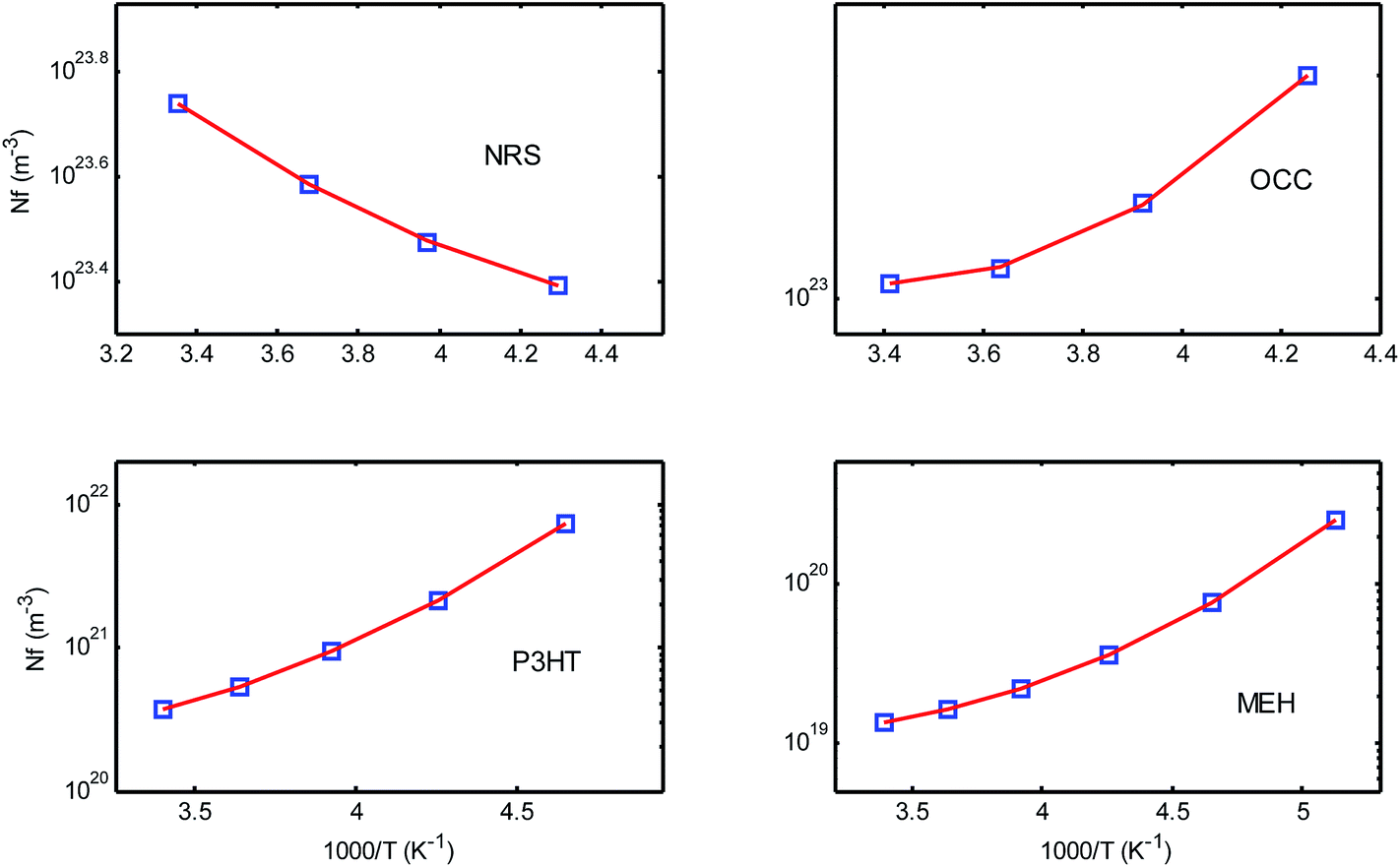 | ||
| Fig. 2 Variations of Nf(T) with temperature, lines are smoothed curves by using eqn (7). | ||
In Fig. 3 and 4, we plot variation of parameters μp(0) and γ with temperature, and curves smoothed by using eqn (8) and (9). The two figures show that eqn (8) and (9) can fit the data points very good. So the analytic J–V formula in eqn (6) with expressions for parameters in eqn (8) and (9) are simple and sound tool for organic diodes. In Fig. 5, we plot percentage errors of smoothed values of Nf, μp(0) and γ relative to values in Table 1. The figure shows that the errors for Nf and γ are always very small, the fitting quality of smoothed curves are fairly good. As for μp(0) the fitting quality is fairly good for two materials NRS-PPV and OC1C10-PPV, merely for other two materials, P3HT and MEH-PPV, the errors are slightly large. Overall speaking, the fitting quality of smoothed values of Nf, μp(0) and γ is satisfactory.
 | ||
| Fig. 3 Variations of μp(0) with temperature, lines are smoothed curves by using eqn (8). | ||
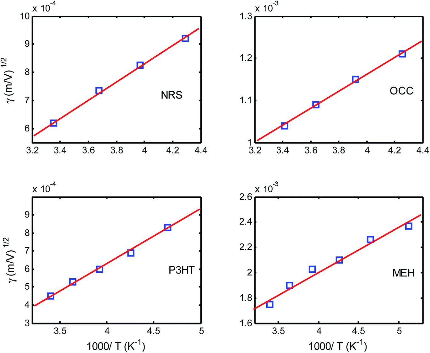 | ||
| Fig. 4 Variations of γ(T) with temperature, lines are smoothed curves by using eqn (9). | ||
 | ||
| Fig. 5 Relative errors of Nf(T) (□), μp(0) (○), and γ(T) (◊) smoothed by using eqn (7)–(9) at different temperature points. | ||
4. Conclusion
In this paper, the electric field dependence of mobility for organic semiconductors is introduced in analytic J–V formula recently proposed by Bruyn et al.,2 and the modified formula is applied to four devices. The results from original formula cannot arrive at good agreement with experimental data. The results from the improved analytic formula are in good agreement with the complete numerical solutions, and both agree with experimental data very good. The modification introduced in this work is necessary; the improved formula is more precise and convenient for applications.Acknowledgements
This work was supported by the Natural Science Foundation of China under Grant no. 10876008, and the Program for Excellent Talents of Sichuan Province of China under Grant no. 2011JQ0053.References
- W. Shockley, Bell Syst. Tech. J., 1949, 28, 435 CrossRef.
- P. de Bruyn, A. H. P. van Rest, G. A. H. Wetzelaer, D. M. de Leeuw and P. W. M. Blom, Phys. Rev. Lett., 2013, 111, 186801 CrossRef CAS.
- A. Salleo, T. W. Chen and A. R. Völkel, et al., Phys. Rev. B: Condens. Matter Mater. Phys., 2004, 70, 115311 CrossRef.
- C. Krellner, S. Haas and C. Goldmann, et al., Phys. Rev. B: Condens. Matter Mater. Phys., 2007, 75, 245115 CrossRef.
- J. Dacuña and A. Salleo, Phys. Rev. B: Condens. Matter Mater. Phys., 2011, 84, 195209 CrossRef.
- S. V. Yampolskii, Y. A. Genenko and C. Melzer, et al., J. Appl. Phys., 2011, 109, 073722 CrossRef PubMed.
- M. Z. Szymanski, I. K. Bajer and J. F. Vincent, et al., Phys. Rev. B: Condens. Matter Mater. Phys., 2012, 85, 195205 CrossRef.
- H. T. Nicolai, M. M. Mandoc and P. W. M. Blom, Phys. Rev. B: Condens. Matter Mater. Phys., 2011, 83, 195204 CrossRef.
- H. T. Nicolai, M. Kuik, G. A. H. Wetzelaer, B. de Boer, C. Campbell, C. Risko, J. L. Brédas and P. W. M. Blom, Nat. Mater., 2012, 11, 882 CrossRef CAS PubMed.
- K. M. Ammar, S. Jiu-Xun, J. Ke, C. Ling-Cang and W. Qiang, RSC Adv., 2015, 5, 3113–3121 RSC.
- D. M. Pai, J. Chem. Phys., 1970, 52, 2285 CrossRef CAS PubMed.
- D. H. Dunlap, P. E. Parris and V. M. Kenkre, Phys. Rev. Lett., 1996, 77, 542 CrossRef CAS.
- W. D. Gill, J. Appl. Phys., 1972, 43, 5033 CrossRef PubMed.
- P. W. M. Blom, M. J. M. de Jong and M. G. van Munster, Phys. Rev. B: Condens. Matter Mater. Phys., 1997, 55, R656 CrossRef CAS.
- W. F. Pasveer, J. Cottaar and C. Tanase, et al., Phys. Rev. Lett., 2005, 94, 206601 CrossRef CAS.
- S. L. M. van Mensfoort and R. Coehoorn, Phys. Rev. B: Condens. Matter Mater. Phys., 2008, 78, 085207 CrossRef.
- L. Jun, S. Jiu-Xun and C. Zhao, Synth. Met., 2009, 159, 1915 CrossRef PubMed.
- X. Bo, S. Jiu-Xun and Y. Kai, et al., J. Polym. Sci., Part B: Polym. Phys., 2012, 51, 1415 Search PubMed.
- Z. Chen-Xin, S. Jiu-Xun, D. Zhi-Jun and Z. Shuai, Semiconductors, 2013, 47, 1361 Search PubMed.
- C. Tanase, E. J. Meijer, P. W. M. Blom and D. M. de Leeuw, Phys. Rev. Lett., 2003, 91, 216601 CrossRef CAS.
| This journal is © The Royal Society of Chemistry 2015 |