
Glycerol as additive in copper indium gallium diselenide electrodeposition: morphological, structural and electronic effects
Francisco Willian de S. Lucas,
Alan R. F. Lima and
Lucia H. Mascaro*
Department of Chemistry, Federal University of São Carlos, São Carlos, São Paulo 13565-905, Brazil. E-mail: lmascaro@ufscar.br; Tel: +55 16 3361 8082
First published on 5th February 2015
Abstract
The co-electrodeposition of copper, indium, gallium and selenium from a pH 1.5 acid bath onto an FTO substrate in the presence of the additive glycerol (GLR) is studied. The concentration of additive in the bath is evaluated, and conditions are optimised for deposition of Cu(In,Ga)Se2 (CIGSe) thin films. The films are characterized by X-ray diffraction (XRD), scanning electron microscopy (SEM), Raman spectroscopy, ultraviolet-visible-near-infrared spectroscopy (UV-Vis-NIR), Mott–Schottky and photocurrent measurements. Mott–Schottky data, XRD and SEM studies reveal an improvement of the crystalline quality and the reduction the number of surface defects of the CIGSe films electrodeposited in presence of the additive. Photo-electrochemical and UV-Vis-NIR measurements show p-type photoconductivity with band gap of 1.34 eV.
1. Introduction
In recent years, the ternary chalcopyrite compounds of the groups I–III–VI direct gap semiconductors, such as CuInSe2 (CISe), have become one of the most promising semiconductor materials for thin film solar cell applications, because of their material properties as an absorber layer for tandem solar cells.1–4 They have also been used for the fabrication of light emitting diodes, optoelectronics and nonlinear optical devices.5 To improve the efficiency of CISe solar cells Al, Ga or S (elements from group III or VI) have been added. With the addition of Ga, the efficiency of CISe solar cells reached 20.3%.2,4 The band gap of the high efficiency CIGSe varies between 1.04 eV and 1.68 eV (1.04 eV to CuInSe2 and 1.68 eV to CuGaSe2). This material also exhibits a high absorption coefficient >105 cm−1 at photon energies above the band gap, which make it ideal for the fabrication of high efficiency thin film photovoltaic devices.2In order to make CIGSe-based solar cells with maximum photovoltaic efficiency and low cost, several techniques have been adopted in CIGSe preparation. The electrodeposition technique is potentially suitable to satisfy this requirement, and it has been used as an alternative method for the growth of a high-quality CIGSe absorber layer. It has some advantages, namely: low cost equipment needs, no use of toxic gases, high deposition rate and scalability for large area substrate coating.1,2,6 This technique has been most intensely investigated and high potential in the opinion of numerous researchers.7–9 Using the strategy mentioned above, in 1999, Bhattacharya et al. of the National Renewable Energy Laboratory (NREL) obtained a new efficiency record of 15.4% using a Cu-rich CIGSe film obtained by electrodeposition as a first step. However, the film composition was found to deviate from the ideal stoichiometry, resulting in the formation of secondary phases.10 Several works dealing with the influence of experimental parameters such as bath composition,1,2,11,12 deposition method1,2,13 and deposition potential1,2,12,14 have been reported in the literature. However, few studies have been devoted to the influence of the presence of non-ionic and non-complexing additives in the electrochemical bath.
The goal of the present work was to study of effect of non-ionic and non-complexing additive in the electrodeposition of CIGSe in order to improve or add new optoelectronic properties to nanostructures. Potentiostatic film growth in a single step using electrodeposition bath with glycerol (GLR) as non-ionic and non-complexing additive is proposed. GLR has been used in alloys plating, resulting in higher deposition efficiency and improvement in the microstructure of deposits.15 In addition, GLR is an inexpensive reagent and, as it is a by-product of biodiesel production, its use is economically and environmentally interesting.15 According to our knowledge, the use of the GLR in the CIGSe thin film electrodeposition has not been reported. Thus, with the aim to gain an insight into the effects of the GLR on electrodeposition of this semiconductor, analysis by cyclic voltammetry, Raman spectroscopy, energy dispersive X-ray, UV-Vis-NIR spectroscopy, scanning electron microscopy, Mott–Schottky, measurements of photocurrent and Rietveld refinement of the X-ray diffraction patterns were conducted.
2. Experimental
Electrochemical investigations were carried out in a potentiostat/galvanostat (Autolab PGSTAT 302N, Metrohm-Eco Chemie) controlled by GPES® and FRA® software. The Ag/AgCl/Cl(sat. KCl)− was used as reference, a Pt-plate as counter and electrodes in a three-electrode configuration electrochemical cell. A plate of fluorine-doped tin oxide (FTO, 7 ohm sq−1, MTI Corporation) coated glass was used as a working electrode. The FTO was cleaned ultrasonically with isopropanol, acetone and ethanol for 15 min in each solvent, then rinsed with deionized water and dried in an N2(g) stream prior to deposition.All electrochemical experiments were conducted without degassing at temperature of 25 ± 2 °C. Cu(In,Ga)Se2 (CIGS) thin films are grown on FTO by single step electrodeposition in aqueous solution. The bath composition was 4 mmol L−1 CuSO4, 2 mmol L−1 In2(SO4)3, 10 mmol L−1 Ga2(SO4)3, 8 mmol L−1 SeO2, 0.5 mol L−1 Na2SO4/H2SO4 – pH 1.5 (as supporting electrolyte). Glycerol (GLR) was used as additive at different concentrations (0, 0.1, 1.0 and 10 mmol L−1). Cyclic voltammetry was used to evaluate the co-deposition process of the elements on FTO. The electrodeposition process was studied at 1 mmol L−1 of the ions in the presence of GLR 10 mmol L−1. Chronoamperometry was performed for the deposition of CIGSe samples in a stationary bath at −0.80 V vs. Ag/AgCl/Cl(sat. KCl)−, for 60 min at 25 °C (total charge of ∼1.59 C). Under these conditions the deposited films had an average thickness of 600 nm. To improve crystallinity of the electrodeposited CIGSe, the films were annealed in a nitrogen atmosphere at 450 °C for 1 h into a not totally gas-tight lead borosilicate glass cylinder (volume 300 mL). For this thermic treatment, a tube furnace was used and the atmosphere outside the cylinder was maintained at 1 atm of N2(g).
The Mott–Schottky experiments were performed in 0.1 mol L−1 NaNO3 by applying a 0.01 Vrms sinusoidal excitation signal with a frequency of 1 kHz. The measurements of photocurrent were also performed in NaNO3 0.1 mol L−1, applying a potential of −0.30 V using a solar simulator with a 150 W xenon lamp (Newport 66902) as a light source and an AM 1.5G lens. Chronoamperograms where obtained at on/off light pulse of 30 s and the light intensity incident on the electrode was adjusted to 100 mW cm−2 (1 sun).
The surface morphology and topology of the films were evaluated by high-resolution field emission scanning electron microscopy (FE-SEM, Zeiss Supra 35 at 2 kV). Semi-quantitative compositional analysis was performed using calibrated energy dispersive X-ray analysis (EDS) (FEI XL30 FEG with an Oxford Instruments – Link ISIS 300 detector). Micro-Raman measurements were made with a Horiba Jobin Yvon (HR 550) system with 514.5 nm wavelength incident argon laser light and coupled with an optical microscope (Olympus BX41) with 10× objective, where the incident laser power was carefully tuned to avoid sample damage or laser induced heating. The crystallographic films characterization was performed with the aid of a X-ray diffractometer (Rigaku – DMax 2500PC) with CuKα radiation, scanning step of 0.02°, counting time of 6 s and 2θ range from 20° to 80°. The size of the crystallographic coherence dominium (D, nm) was estimated from the (220) CIGSe peak by the Scherrer equation, where the line broadening for the instrumental effects was corrected with the silicon powder standard (99%, 325 mesh, SRM-640) by Caglioti equation, as described by Gonçalves et al.16 All samples were refined by the Rietveld method17 through the GSAS program.18 The input data of the theoretical model were those available in the Inorganic Crystal Structure Database (ICSD).19 UV-Vis-NIR spectroscopy with diffuse reflectance geometry was carried out in a Cary 5E spectrometer from 200 to 2500 nm to determine the band gap energy of the films.
3. Results and discussion
3.1 Electrochemical deposition potentials study
One exploratory voltammetric study was made in bath solution composed of 1 mmol L−1 of each electroactive specie (Cu2+, In3+, Ga3+ and HSeO3−) and 0.5 mol L−1 Na2SO4/H2SO4 – pH 1.5 (as supporting electrolyte) in the absence and presence of 10 mmol L−1 GLR (used as additive). The cyclic voltammograms obtained for this quaternary system can be seen in Fig. 1. | ||
| Fig. 1 Cyclic voltammograms on FTO and at scan rate of 50 mV s−1 for the solution constituted of HSeO3−, Cu2+, In3+ and Ga3+ (1 mmol L−1, each) in H2SO4 0.5 mol L−1. In additive absence (solid line) and containing GLR 10 mmol L−1 (dashed line). | ||
The cyclic voltammograms in Fig. 1 show the crossover characteristic of three-dimensional nucleation and have well-defined four cathodic and two anodic stripping peaks. The complexity of this system does not allow for assigning one single specified process of reduction or oxidation at each peak. However, we can infer the possible deposited species by comparing the peak potentials obtained in our study with those observed in the literature for pure metals or mixtures. In cathodic sweep, the peaks C1 and C2 at −0.2 V and −0.42 V, respectively, can be attributed to the co-reduction of Cu2+ and HSeO3− with formation of different CuxSey binary phases.20–22 The peak C3 could be related to deposition of CuxIny and/or InxSey phases.20,21 By the last the peak C4 appear at potential region characteristic of growth of GaxSey phase and reduction of Se0 to H2Se.20–22 In presence of additive, there was no significant peak potentials shift of these processes, indicating that the additive did not form complexes with ions of the electrolytic bath.
Based on cyclic voltammetry results, the potential of −0.8 V was chosen for electrodeposition of the films. This potential is more negative than all cathodic peaks observed in Fig. 1 and the formation of In, Ga and Cu selenides and/or CIGSe phases is expected. No significant difference was observed in the deposition chronoamperogram with GLR addition and the total charge was of ∼1.59 C.
3.2 Structural and morphological properties
In order to identify which phases were formed during the process of electrodeposition, Raman spectroscopy and X-ray Diffraction (XRD) techniques were used. The NADT (without additive), 0.1GLR, 1GLR and 10GLR CIGSe coatings were grown using 0, 0.1, 1.0 and 10 mmol L−1 of GLR, respectively. The Raman spectra of the CIGSe films obtained at different GLR concentration can be seen in Fig. 2. | ||
| Fig. 2 Raman spectrum of the films (a) NADT, (b) 0.1GLR, (c) 1GLR and (d) 10GLR. | ||
The main part of these spectra is situated between 100 cm−1 and 450 cm−1. For all films, the presence of a most intense peak at about 174 cm−1 can be evidently observed, which can be attributed to the A1 symmetry vibrational mode of CIGSe resulting from the Se atom motion in the x–y plane with others atoms at rest.13,23–26 The smallest full width at half maximum (FWHM) of the 174 cm−1 peak was observed for the films 1GLR and 10GLR, evidencing that these had a greater level of bulk crystallinity (the data can be seen in Table 1). Also, shoulders in the region of 213 to 230 cm−1 were observed, which can be related to the mixing of phonon modes of B2 and E symmetries of the chalcopyrite phase.23 In Raman spectrum of the films NADT and 1GLR, a shoulder was also observed at about 154 cm−1 that can be evidence of the formation of ordered vacancies compounds (OVCs) attributed to the existence of complex point defects in the chalcopyrite structure.25 Moreover, it should be noted that there is no additional peak at 258 cm−1 related to the presence of a highly conductive CuxSe phase or presence of bands associated with elemental Se, around 240 cm−1, which would indicates the films are suitable for the production of efficient solar cells.13,23–26 However, this does not mean that these phases are not present; it could be that the high Raman scattering of the majority phase (CIGSe) has suppressed the secondary phases.
| CIGSe | Phasesa | RR parameters | D (nm) | FWHM (cm−1) | |||||
|---|---|---|---|---|---|---|---|---|---|
| CIGSe (majority) | CuSe | InSe | Se | Rwp (%) | RBragg (%) | χ2 | |||
| a ICSD code phases: CIGSe (163564), CuSe (59955), InSe (1376) and Se (24635). The FTO (SnO2 cassiterite phase, 90611) phase was present in all films. D was calculated from the (220) peak and FWHM from A1 mode of the CIGSe phase. | |||||||||
| NADT | X | X | — | X | 3.08 | 1.03 | 3.05 | 14.98 | 14.7 |
| 0.1GLR | X | X | X | — | No refined | — | 14.3 | ||
| 1GLR | X | — | — | — | 4.56 | 4.56 | 3.41 | 32.71 | 9.54 |
| 10GLR | X | X | — | — | 5.81 | 4.89 | 3.87 | 25.41 | 9.67 |
In addition to the conclusions obtained from the Raman spectrum and to verify the presence of secondary phases, Rietveld refinement (RR) of the CIGSe films diffraction patterns was performed. In Fig. 3 are shown the experimental and calculated X-ray diffraction patterns from refinements made by the Rietveld method of the NADT and 1GLR films. Most of the qualitative and statistical results obtained by RR are summarized in Table 1.
 | ||
| Fig. 3 Experimental and calculated X-ray diffraction patterns of the (a) NADT and (b) 1GLR films. | ||
In all the refinements, the RBragg index presented satisfactory low values, indicating a good refined crystal structure model representative of the real case. The residual pattern shows that there is a good match between the theoretical and observed XRD patterns, noted by the small variation along the diffraction angle as shown in Fig. 3, as is also evidenced by the Rwp and χ2 index values shown in Table 1. Thus, by comparison with patterns available in the Inorganic Crystal Structure Database (ICSD),19 it was observed that the majority phase present in all films was the CIGSe [ICSD code: 163564, space group: I![[4 with combining macron]](https://www.rsc.org/images/entities/char_0034_0304.gif) 2m (121)]. The presence of secondary phases that were not identified in the Raman spectra were also observed, such as: Cu2Se [ICSD code: 59955, space group: F23(196)], In2Se3 [ICSD code 1376, space group P61(169)] and Se [ICSD code: 24635, space group: P121/c1(14)]. In Table 1, the phases present in each film were identified and, as can be seen, only the 1GLR film did not present bulk secondary phases.
2m (121)]. The presence of secondary phases that were not identified in the Raman spectra were also observed, such as: Cu2Se [ICSD code: 59955, space group: F23(196)], In2Se3 [ICSD code 1376, space group P61(169)] and Se [ICSD code: 24635, space group: P121/c1(14)]. In Table 1, the phases present in each film were identified and, as can be seen, only the 1GLR film did not present bulk secondary phases.
From (220) peak of the majority phase, the size of the crystallographic coherence dominium (D) of the films was estimated and the data were organized in Table 1. Agreeing with the observations from Raman spectra, one of the less crystalline films was the NADT, i.e., with smaller D. The more crystalline film was the 1GLR, observing that the use of additive also improved the crystallinity of the films, one of the more important properties required for films used in photovoltaic devices.
The morphological characteristics of the films were observed by Scanning Electron Microscopy (SEM). The SEM micrographs of the film obtained from bath in absence and presence of additive are shown in Fig. 4.
 | ||
Fig. 4 SEM micrographs with magnification of 100![[thin space (1/6-em)]](https://www.rsc.org/images/entities/char_2009.gif) 000× of the CIGSe films (a) NADT, (b) 0.1GLR, (c) 1GLR and (d) 10GLR. 000× of the CIGSe films (a) NADT, (b) 0.1GLR, (c) 1GLR and (d) 10GLR. | ||
From Fig. 4, it can be concluded that the additive promotes changes in the films grain size, despite all films showing a very compact and homogeneous surface morphology, having some clusters with roughly uniform size and globular aspects. The 10GLR–CIGSe film showed less compact morphology with large grains.
Associated with SEM, semi-quantitative analyses of the films' composition were carried out by energy-dispersive X-ray spectroscopy (EDX); the data were organized in Table 2.
| CIGSe | Eg (eV) | Atomic composition (% atm.) | Mott–Schottky | ||||
|---|---|---|---|---|---|---|---|
| Cu | In | Ga | Se | Efba (V) | NDb (cm−3) | ||
| a E vs. Ag/AgCl/Cl(sat. KCl)−.b For calculation was used εs = 13.5 (ref. 33). | |||||||
| NADT | 1.34 | 10 | 23 | 1.2 | 66 | −0.92 | 5.37 × 10²⁰ |
| 0.1GLR | 1.35 | 10 | 30 | 0.7 | 59 | −0.56 | 5.00 × 10¹⁹ |
| 1GLR | 1.34 | 15 | 28 | 0.7 | 57 | −0.66 | 1.17 × 10²⁰ |
| 10GLR | 1.34 | 25 | 22 | 1.1 | 52 | −0.85 | 2.44 × 10²¹ |
From Table 2, it was possible to conclude that when GLR is added to electrodeposition bath, the Cu/In ratio of the films has obviously increased from 0.33 to 1.13, while the Se/(Cu + In) ratios were always greater than 1 in the conditions studied. Although, no change was observed at voltammograms as shown in Fig. 1, the presence of GLR changed the deposit composition. In general, the electrodeposition conditions used in this work promoted a formation of In-rich CIGSe films and with low Ga content. Despite the near-stoichiometric composition (Cu: 25%, In: 22% and Se: 52%) obtained when the electrodeposition was performed at 10GLR, DRX results shown that the CIGSe and CuSe phases were deposited in the experimental conditions.
3.3 Physical and optical properties
In order to determine optical band gap of the obtained CIGSe thin film, the sample was prepared as described above. The band-gap energy (Eg) was determined by UV-Vis-NIR diffuse reflectance spectroscopy (DRS) using the following equation:27
 | (1) |
In Fig. 5, the graphs of (αhν)2 can be seen as a function of hν, being the Eg values determined by extrapolating the linear region, as shown in eqn (1) for a allowed direct transition, i.e., n equals 2. The Eg of the films were organized in Table 2.
 | ||
| Fig. 5 Graph of (αhν)2 versus hν for the CIGSe films. | ||
The values of Eg found at about 1.35 eV are similar to those reported in the literature of CIGSe films,15 indicating that the Ga content was sufficient for the formation of CIGSe quaternary phases. For a ternary CuInSe2 system, the value of Eg should be about 1.04 eV,1 a value much lower than that obtained in our work, which reinforces that it was formed in the quaternary phase and not the ternary phase.
In order to characterize the physical properties of these films, the flat band potential (Efb), the charge carriers density (ND) and the semiconductor type (n- or p-) were determined by the Mott–Schottky equation. The results were obtained by potentiodynamic electrochemical impedance spectroscopy experiments and described by the following equation:28–30
 | (2) |
Using the Mott–Schottky graph, the ND can be calculated from the slope and the Efb can be obtained from the extrapolation to CSC2− = 0. The CIGSe thin films were prepared and capacitance data were obtained in 0.1 mol L−1 NaNO3 by applying a 0.01 Vrms sinusoidal excitation signal with frequency of 1 kHz. The Mott–Schottky graph for the 1GLR film, ND and Efb values can be seen in Fig. 6 and in Table 2, respectively.
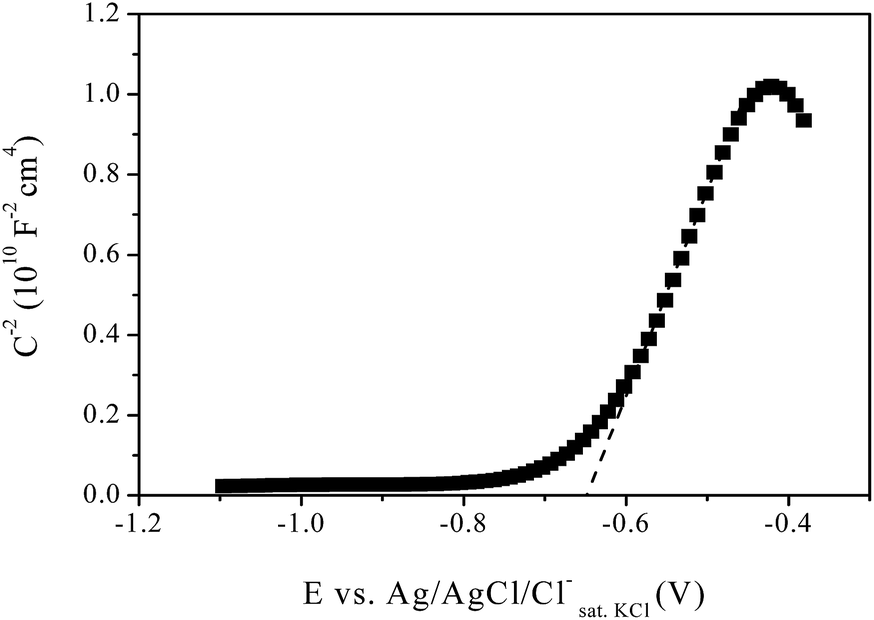 | ||
| Fig. 6 Mott–Schottky graph for the 1GLR film performed in NaNO3 0.1 mol L−1 by applying a sinusoidal excitation of 0.01 Vrms with frequency of 1 kHz. | ||
Based on the slope of the Mott–Schottky graph, it can be proven that all obtained films were n-type semiconductors, since the slope was positive in all cases.28–30 This behaviour is expected for In-rich CIGSe films, as observed by Djellal et al.31 Their films also showed Efb and ND values of −0.74 V vs. Ag/AgCl/Cl(sat. KCl)− and 2.73 × 10¹⁹, respectively. As can be seen in Table 2, the 1GLR film showed Efb values closer to those reported, i.e., this film had electronic structure closer to the films obtained by that good quality method. The high ND observed for these electrodeposited films can be related to small clusters observed by SEM on the film surface. These structures can be constituted by CuxSe crystals and increase the defects density on the surface, causing the high ND values observed, as similarly argued by Valdés and et al.32 Since the Mott–Schottky plot describes predominantly the electronic behaviour on the surface,33 the films that had fewer surface defects were 0.1GLR and 1GLR. The 10GLR showed an extremely higher number of surface defects than other films.
Fig. 7 illustrates the photocurrent chronoamperograms curve of the deposited CIGSe film. This figure exhibits a cathodic photocurrent, which is a characteristic of a semiconductor with p-type conductivity opposite to that seen by the Mott–Schottky plot. The same behaviour was observed by Sebastian et al.33 where the existence of p–n junction at CIGSe surface was considered with an empirical model for superficial and bulk conductivity. Thereby, photocurrent measurement is due to the conduction effect in the bulk of the film, and Mott–Schottky data is relative to superficial conduction. In other words, it is correct to say that the film is p-type conducting in the bulk. Further analysing Fig. 7, we can see that the highest and lowest values of the photocurrent intensity were obtained when the samples were obtained from the electrodeposition bath containing 1GLR and 10GLR, respectively. Thus, increasing grain boundary and superficial defects will increase charge recombination and the photocurrent will decrease. We can also conclude that when the secondary phase is present in the film, there is a higher probability of recombination of charge, and the photocurrent decreases. The results are in agreement with data DRX, SEM and Mott–Schottky data. Therefore, the optimal crystal size and pure phase of the semiconductor thin films is very important for photovoltaic system application.
 | ||
| Fig. 7 Chronoamperograms of the photocurrent study (light 30 s on/off) in NaNO3 0.1 mol L−1, applying a potential of −0.30 V. The light intensity incident on the electrode was adjusted to 100 mW cm−2 and the solar spectra was simulated with an AM 1.5G lens. | ||
Summarizing all previous characterizations, the NADT and 0.1GLR films present a greater amount of secondary phases and lower bulk crystallinity, which justifies its high surface defects level (identified by the value of ND) and the Efb being so different from the other films (see Table 1). In contrast, the optimised condition of electrodeposition was achieved with the used of 1 mM GLR in electrolytic bath, providing the reduction of the number of surface defects, secondary phases and the increase of the size of crystallographic coherence dominium as well as the crystallinity of the CIGSe film.
4. Conclusions
A simple addition of non-ionic and non-complexing additive can change the film morphology/microstructure, causing interesting effects in its electronics properties. All characterizations led to the conclusion that, compared to CIGSe film obtained without addition of the additive, the presence of 1 mM Glycerol provides a reduction in the number of surface defects, of secondary phases and improves the bulk crystallinity of the electrodeposited CIGSe films.Acknowledgements
We wish to thank the São Paulo Research Foundation (FAPESP), grant 2012/10947-2, 2013/07296-2 and INCTMN 2008/57872-1 CNPq 573636/2008-7.References
- D. Lincot, J. F. Guillemoles, S. Taunier, D. Guimard, J. Sicx-Kurdi, A. Chaumont, O. Roussel, O. Ramdani, C. Hubert, J. P. Fauvarque, N. Bodereau, L. Parissi, P. Panheleux, P. Fanouillere, N. Naghavi, P. P. Grand, M. Benfarah, P. Mogensen and O. Kerrec, Sol. Energy, 2004, 77, 725–737 CrossRef CAS PubMed
.
- V. S. Saji, I.-H. Choi and C.-W. Lee, Sol. Energy, 2011, 85, 2666–2678 CrossRef CAS PubMed
- F. Roux, S. Amtablian, M. Anton, G. Besnard, L. Bilhaut, P. Bommersbach, J. Braillon, C. Cayron, A. Disdier, H. Fournier, J. Garnier, A. Jannaud, J. Jouhannaud, A. Kaminski, N. Karst, S. Noël, S. Perraud, O. Poncelet, O. Raccurt, D. Rapisarda, A. Ricaud, D. Rouchon, M. Roumanie, E. Rouviere, O. Sicardy, F. Sonier, K. Tarasov, F. Tardif, M. Tomassini and J. Villanova, Sol. Energy Mater. Sol. Cells, 2013, 115, 86–92 CrossRef CAS PubMed
- K. G. Deepa, N. Lakshmi Shruthi, M. Anantha Sunil and J. Nagaraju, Thin Solid Films, 2014, 551, 1–7 CrossRef CAS PubMed
- S. Hamrouni, M. S. AlKhalifah, M. F. Boujmil and K. Ben Saad, Appl. Surf. Sci., 2014, 292, 231–236 CrossRef CAS PubMed
- F. Kang, J. P. Ao, G. Z. Sun, Q. He and Y. Sun, Mater. Chem. Phys., 2009, 115, 516–520 CrossRef CAS PubMed
- N. P. Klochko, G. S. Khrypunov, N. D. Volkova, V. R. Kopach, a. V. Momotenko and V. N. Lyubov, Semiconductors, 2014, 48, 521–530 CrossRef CAS
- Y. Wang, H. Nie and S. Guo, Rare Met., 2010, 29, 519–523 CrossRef CAS
- X. Wang, G. Wang, B. Tian, S. Wan and Z. Du, Chin. Sci. Bull., 2010, 55, 1854–1858 CrossRef CAS PubMed
- R. N. Bhattacharya, W. Batchelor, J. F. Hiltner and J. R. Sites, Appl. Phys. Lett., 1999, 75, 1431–1433 CrossRef CAS PubMed
- O. Meglali, N. Attaf, a. Bouraiou, J. Bougdira, M. S. Aida and G. Medjahdi, J. Alloys Compd., 2014, 587, 303–307 CrossRef CAS PubMed
- H. Lee, H. Yoon, C. Ji, D. Lee, J.-H. Lee, J.-H. Yun and Y. Kim, J. Electron. Mater., 2012, 41, 3375–3381 CrossRef CAS PubMed
- M. Valdés and M. Vázquez, J. Solid State Electrochem., 2012, 16, 3825–3835 CrossRef PubMed
- S. I. Bocharova, M. V. Gapanovich, D. N. Voilov, I. N. Odin and G. F. Novikov, Nanotechnol. Russ., 2013, 8, 292–296 CrossRef
- G. A. G. Pedroza, C. A. C. de Souza, I. A. Carlos and L. R. P. de Andrade Lima, Surf. Coat. Technol., 2012, 206, 2927–2932 CrossRef CAS PubMed
- N. S. Gonçalves, J. A. Carvalho, Z. M. Lima and J. M. Sasaki, Mater. Lett., 2012, 72, 36–38 CrossRef PubMed
- R. A. Young, The Rietveld method, Oxford University Press, London, 1995 Search PubMed
- A. C. Larson and R. B. Von Dreele, General Structure Analysis System (GSAS), 1994, vol. 748 Search PubMed
- Inorganic Crystal Structure Database, available at, http://www.fiz-karlsruhe.de/icsd.html.
- J. Liu, F. Liu, Y. Lai, Z. Zhang, J. Li and Y. Liu, J. Electroanal. Chem., 2011, 651, 191–196 CrossRef CAS PubMed
- Y. Li, S. S. Shaikh and S. Menezes, Thin Solid Films, 2012, 524, 20–25 CrossRef CAS PubMed
- F. W. d. S. Lucas, A. R. F. Lima and L. H. Mascaro, Electrochim. Acta, 2014, 147, 47–53 CrossRef CAS PubMed
- A. Bhatia, H. Meadows, W. M. Hlaing Oo, P. J. Dale and M. A. Scarpulla, Thin Solid Films, 2013, 531, 566–571 CrossRef CAS PubMed
- O. Ramdani, J. F. Guillemoles, D. Lincot, P. P. Grand, E. Chassaing, O. Kerrec and E. Rzepka, Thin Solid Films, 2007, 515, 5909–5912 CrossRef CAS PubMed
- Y.-H. Su, T.-W. Chang, W.-H. Lee and B.-H. Tseng, Thin Solid Films, 2013, 535, 343–347 CrossRef CAS PubMed
- M. Valdés, M. Mollar, M. Vázquez and B. Marí, J. Appl. Electrochem., 2013, 43, 619–628 CrossRef
- M. Nowak, B. Kauch and P. Szperlich, Rev. Sci. Instrum., 2009, 80, 046107 CrossRef CAS PubMed
- K. Gelderman, L. Lee and S. W. Donne, J. Chem. Educ., 2007, 84, 685–688 CrossRef CAS
- W. J. Albery, G. J. O'Shea and A. L. Smith, J. Chem. Soc., Faraday Trans., 1996, 92, 4083–4085 RSC
- A. W. Bott, Curr. Sep., 1998, 17, 87–91 CAS
- L. Djellal, M. Doulache and M. Trari, Semicond. Sci. Technol., 2011, 26, 085034 CrossRef
- M. H. Valdés and M. Vázquez, Electrochim. Acta, 2011, 56, 6866–6873 CrossRef PubMed
- P. Sebastian, M. Calixto, R. Bhattacharya and R. Noufi, Sol. Energy Mater. Sol. Cells, 1999, 59, 125–135 CrossRef CAS
| This journal is © The Royal Society of Chemistry 2015 |