DOI:
10.1039/C4RA16311G
(Paper)
RSC Adv., 2015,
5, 40283-40296
Simplistic construction of cadmium sulfoselenide thin films via a hybrid chemical process for enhanced photoelectrochemical performance†
Received
13th December 2014
, Accepted 13th April 2015
First published on 13th April 2015
Abstract
We have successfully synthesized cadmium sulfoselenide (Cd(S1−xSex)) thin films via a simplistic and promising self-organized chemical growth process for photoelectrochemical (PEC) application. The effects of bath composition on the optical, structural, morphological, and electrical properties and the photoelectrochemical performance of (Cd(S1−xSex)) thin films have been investigated. Deposited thin films were characterized using UV-Vis spectrophotometry, X-ray diffraction (XRD), high-resolution transmission electron microscopy (HRTEM) with a selected area electron diffraction (SAED) pattern, field-emission scanning electron microscopy (FESEM) coupled with energy dispersive X-ray spectroscopy (EDS), X-ray photoelectron spectroscopy (XPS), electrical conductivity (EC) and thermoelectric power (TEP) measurement techniques. An optical absorption study showed that the maximum light absorption in the 630–720 nm wavelength range and the linear nature of absorption plots indicate that the transition is a direct allowed type. The optical band gap energy decreased from 2.13 to 1.71 eV with varying bath composition. The XRD study illustrated that deposited thin films are in the pure phase with a nanocrystalline nature. HRTEM images highlight the formation of clearly-defined, interconnected particle, which aggregated to form a well-grown custard apple-like morphology over the entire substrate and are in good accordance with FESEM micrographs. The SAED pattern shows a ring pattern indicating the nanocrystalline nature of the deposited thin film. The FESEM study demonstrated that the developed surface morphology is favorable for effectual light absorption in the solar spectrum. The XPS analysis specified the presence of Cd2+, S2− and Se2− elements in the deposited thin film. The EDS spectrum confirmed that thin film deposition occurs in a stoichiometric manner. From the EC measurement study, it was observed that electrical conductivity increases correspondingly for all thin films, indicating semiconducting behavior. TEP measurements established that Cd(S1−xSex) thin films are n-type in nature. Finally, the deposited thin films were tested for photoelectrochemical (PEC) application. The PEC study illustrated that (Cd(S0.2Se0.8)) thin film showed the highest power conversion efficiency (η) of 1.02% among reported values.
1. Introduction
The environmental benign, cost effective and alternative energy sources are global need.1 An extreme reliance on various non-renewable energy sources brings not only an economical problem but also affects the globe economy and civilization.2,3 Considering these facts, it is necessary to develop cost effective and efficient solar cell devices.4 Commonly, energy conversion and storage devices include solar cells,5,6 fuel cells,7 photoelectrochemical water splitting cells,8 Li-ion batteries and supercapacitors.9 The performance of such energy devices is dependent on the different properties of the nanostructured metal chalcogenide.1 Progressive fabrications of novel nanostructures with different sizes and new morphologies offer wide applicability of metal chalcogenide thin films. As the size of metal chalcogenides is reduced to the nanometer-scale, synergetic chemical and physical properties emerge owing to the well-known quantum size effect.10 Also, nanostructured metal chalcogenides can provide a higher effective surface area compared to bulk counterparts, which is beneficial for power conversion efficiency.11
Nanocrystalline materials possess typical chemical and physical properties that are relevant for the development of promising devices.12 Recently, the IIB–VIA semiconducting groups of ternary, quaternary and multinary thin films have attracted immense attention because of their tremendous use in opto-electronic devices.13 IIB–VIA semiconductors are generally characterized by a direct optical band gap covering the entire visible region of the solar spectrum from infrared to ultraviolet.13–16 Among the IIB–VIA group semiconducting chalcogenides, ternary Cd(S1−xSex) thin films are pseudo binary compounds of CdS and CdSe.16 Ternary Cd(S1−xSex) thin films are widely used due to their important properties such as a high absorption coefficient, high efficiency of radiative recombination and nearly well-matched optical band gap with the visible region of the solar spectrum (1.0–3.0 eV).17 CdSe (1.7 eV) and CdS (2.4 eV) belong to the IIB–VIA group, and they are most widely used semiconductor materials for CdTe/CdSe and CdTe/CdS hetero-junction photovoltaic devices.18 They also act as a window layer in copper indium disulfide (CIS)19 as well as copper indium gallium sulfide (CIGS).20,21 Ternary Cd(S1−xSex) materials have promising properties in solar cell application.22 The incorporation of selenium in cadmium sulfide thin films lowers the band gap energy and enhances absorption and spectral sensitivity, which are beneficial for light harvesting in the visible region of the solar spectrum.23,24
Cd(S1−xSex) ternary thin films have been prepared by using various techniques, such as chemical bath deposition (CBD),25,26 the metal catalyzed vapor liquid method,27 screen printing followed by sintering,28 hot wall epitaxy,29 pulse printing,30 a solvothermal route31 and sputtering.32 Conversely, these methods require harsh experimental conditions, a toxic reducing agent, organic surface directing agents, solvents and highly sophisticated instruments. In the present investigation, we have used the arrested precipitation technique (APT) for the deposition of ternary Cd(S1−xSex) thin films. The APT is a self-organized, facile, cost effective method for large area thin film deposition and does not require sophisticated instruments unlike other chemical techniques. Also, APT is hybrid chemical process of CBD and the controlled chemical growth process (CCGP).33,34 To date, Cd(S1−xSex) ternary thin films have been used in various fields of applications such as photoelectrochemical solar cells,22 photovoltaics,35 visible light-emitting diodes, lasers,36 environmental sensors and photo-detectors.37 Taking into account the extensive significance of ternary Cd(S1−xSex) thin films, we have synthesized ternary Cd(S1−xSex) thin films using triethanolamine (TEA) as a complexing agent with varying bath composition via APT.
In our previous report, we successfully developed pure phase nanocrystalline Cd(SSe) thin films by using a self-organized APT method. In this attempt, we have deposited Cd(SSe) thin films at different deposition times using TEA as a complexing agent. The results clearly indicate that deposition time plays a crucial role in the growth process as well as the fabrication of good-quality thin films. An overall literature survey highlights that varying the bath composition is important for optimization of properties and construction of high-efficiency thin films. Hence, in the present investigation, we tried to vary bath composition to obtain high-efficiency Cd(S1−xSex) thin films.
To the best of our knowledge and the literature survey, there is no single report available on the development of unique surface morphologies of Cd(S1−xSex) thin films achieved by varying the bath composition via APT. The main aim of this report is to optimize and construct a morphological growth pathway by varying bath compositions for maximum light absorption capability. Also, we have checked the PEC performance with the highest conversion efficiency 1.02%. The detailed growth mechanism and PEC working mechanism of Cd(S1−xSex) thin films are presented in this article.
2. Experimental
2.1 Materials and methods
All chemicals were analytical reagent (AR) grade and used without further purification. Cadmium sulfate monohydrate (CdSO4·H2O; 98%, s-d Fine Chem.), thiourea (H2N–CS–NH2; 99%, s-d Fine Chem.), selenium metal powder (99.5%, Sigma Aldrich), sodium sulfite (Na2SO3; 96%, s-d Fine Chem.), liquor ammonia (NH3; 28–30% Thomas Baker), and triethanolamine (N(CH2–CH2–OH)3; 99%, Merck) were used as precursors and the complexing agent. For measurement of PEC properties, we have used sulfide/polysulfide redox electrolyte (0.5 M) prepared from sodium sulfide (Na2S; Thomas Baker), sodium hydroxide pellets (NaOH; 99%, s-d Fine Chem.) and sulfur powder (99%, s-d Fine Chem.), etc. Indium-tin oxide (ITO)-coated glass substrates were ultrasonically cleaned using detergent followed by methanol treatment and finally cleaned with acetone and deionized water.
2.2 Thin film synthesis
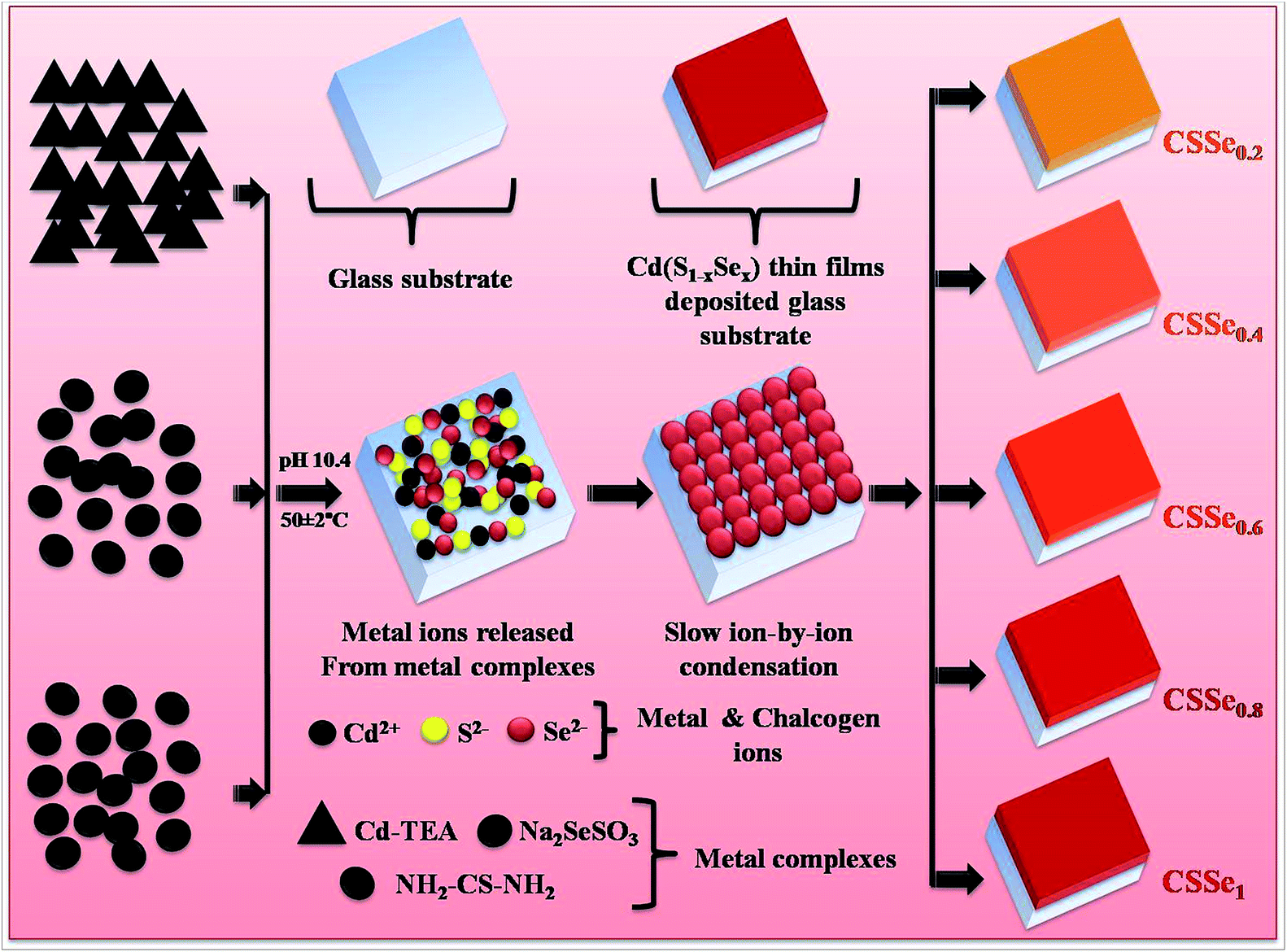
In the typical synthesis process, a solution of 0.05 M Cd–TEA complex was used as a source of Cd2+ ions, where CdSO4·H2O was triturated with TEA as a complexing agent for 6 h to form a clear solution of the Cd–TEA complex. Sodium selenosulfite (Na2SeSO3) was prepared by refluxing selenium metal powder with anhydrous sodium sulfite at 90 °C for 8 h. Cd–TEA complex was reacted with S2− and Se2− ions, which are released slowly by ion-by-ion condensation from the dissociation of H2N–CS–NH2 and Na2SeSO3 at alkaline pH 10.4 and 50 ± 2 °C.
Nucleation and thin film formation depend on various preparative parameters such as the complexing agent, precursor concentration, pH, deposition time and bath temperature. These parameters were optimized during the initiative stage of thin film deposition. Precursor concentration was kept invariable as 0.05 M, and bath composition varied from Cd(S0.8Se0.2), Cd(S0.6Se0.4), Cd(S0.4Se0.6), Cd(S0.2Se0.8) and Cd(S0.0Se1.0) at the optimized deposition time of 2.30 h. At the terminal growth phase, all the deposited thin films were yellowish, yellowish orange, light red and dark red in colour (Scheme 1), respectively, and well adherent to the substrates. The deposited films were correspondingly designated as, CSSe0.2, CSSe0.4, CSSe0.6, CSSe0.8 and CSSe1.0, respectively. The optimized preparative and compositional parameters were tabulated in Table 1.
 |
| | Scheme 1 Probable growth mechanism of Cd(S1−xSex) thin films formed via the APT method. | |
Table 1 Optimized preparative parameters for the synthesis of Cd(S1−xSex) thin films
| Sample code |
Bath composition |
Volume of ‘Cd’ precursor (mL) |
Volume of ‘S’ precursor (mL) |
Volume of ‘Se’ precursor (mL) |
| CSSe0.2 |
CdS0.8Se0.2 |
20 |
16 |
04 |
| CSSe0.4 |
CdS0.6Se0.4 |
20 |
12 |
08 |
| CSSe0.6 |
CdS0.4Se0.6 |
20 |
08 |
12 |
| CSSe0.8 |
CdS0.2Se0.8 |
20 |
04 |
16 |
| CSSe1.0 |
CdS0.0Se1.0 |
20 |
00 |
20 |
2.3 Characterization of thin films
The thickness of deposited thin films was measured using a surface profiler (AMBIOS XP-1). The optical absorption was measured using a UV-Vis spectrophotometer (Shimadzu, UV-1800). Structural properties were studied by using an X-ray diffractometer (Bruker AXS, D8) using Cu Kα (λ = 1.5418 Å) radiation for 2θ ranging from 20° to 70°. The structural and morphological analysis was carried out using high resolution-transmission electron microscopy (HRTEM). The surface morphology and elemental composition of the deposited thin films were assessed by field-emission scanning electron microscopy (FESEM) using a microscope equipped with an energy dispersive X-ray spectroscopy (EDS) analyzer [S-4700, Hitachi]. Elemental information concerning the deposited thin films was analyzed by using an X-ray photoelectron spectrometer (XPS, Thermo Scientific, Multilab-2000) with a multi-channel detector, which can endure high photon energies from 0.1–3 keV. The electrical conductivity (EC) of the deposited thin films was measured by a two-probe method. Thermoelectric power (TEP) measurements were taken under conditions of maximum temperature difference and minimum contact resistance using a C-T meter (Teleph-France) apparatus. PEC performance was carried out using a semiconductor parameter analyzer (Keithley SCS-4200 Semiconductor) characterization unit in dark and under illumination using a 500 W tungsten filament lamp (intensity of 30 mW cm−2) in 0.5 M sulfide/polysulfide redox electrolyte. A PEC cell was fabricated using the standard two-electrode configuration and comprised a glass-ITO/Cd(S1−xSex) (active surface area 1 cm2) photoelectrode and a graphite rod as the counter electrode. All measurements were taken at room temperature (300 K).
3. Results and discussion
3.1 Growth mechanism of thin film formation
In arrested precipitation, metal ions are arrested by using TEA as a complexing agent and metal ions released at the optimized precursor concentration, pH and temperature. Aqueous ammonia was used to optimize the pH, which is a method to increase the concentration of OH− ions and increase the relative molecular area and solubility of S2− and Se2− ions in the reaction bath.31
The temperature of bath solution was also optimized (2.30 h), for the reason that at a higher temperature more metal ions are released and the reaction rate gets faster, which results in bulk precipitation rather than the desired thin film formation.32 To achieve high-quality, pin-hole free thin films, we have optimized the precursor concentrations, pH, temperature and deposition time as 0.05 M, 10.4, 50 °C and 2.30 h, respectively.
APT is based on the Ostwald ripening law.38 According to this law, the rate of reaction between metal ions along with chalcogen ions can be controlled by using stable TEA as a complexing agent. Smaller nuclei or embryos come toward each other and form a large crystal. With increased deposition time, additional metal ions will be released as well as dissolution of smaller particles, and well-grown large crystals are obtained. Creation of Cd(S1−xSex) thin film occurs when the ionic product (Kp) exceeds the solubility product (Ksp) of metal ions and a multi-nucleation process occurs next to ion-by-ion condensation of metal and chalcogen ions onto the substrate surface39. A detailed growth mechanism of Cd(S1−xSex) thin film formation and the effect of bath composition is provided in Scheme 1.
A detailed proposed possible reaction mechanism for cadmium sulfoselenide thin films was recently discussed.33 Finally, deposited Cd(S1−xSex) thin films were well adherent to the bare and ITO-coated glass substrates.
3.2 Optical absorption data
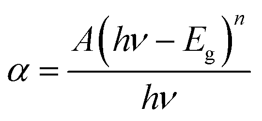
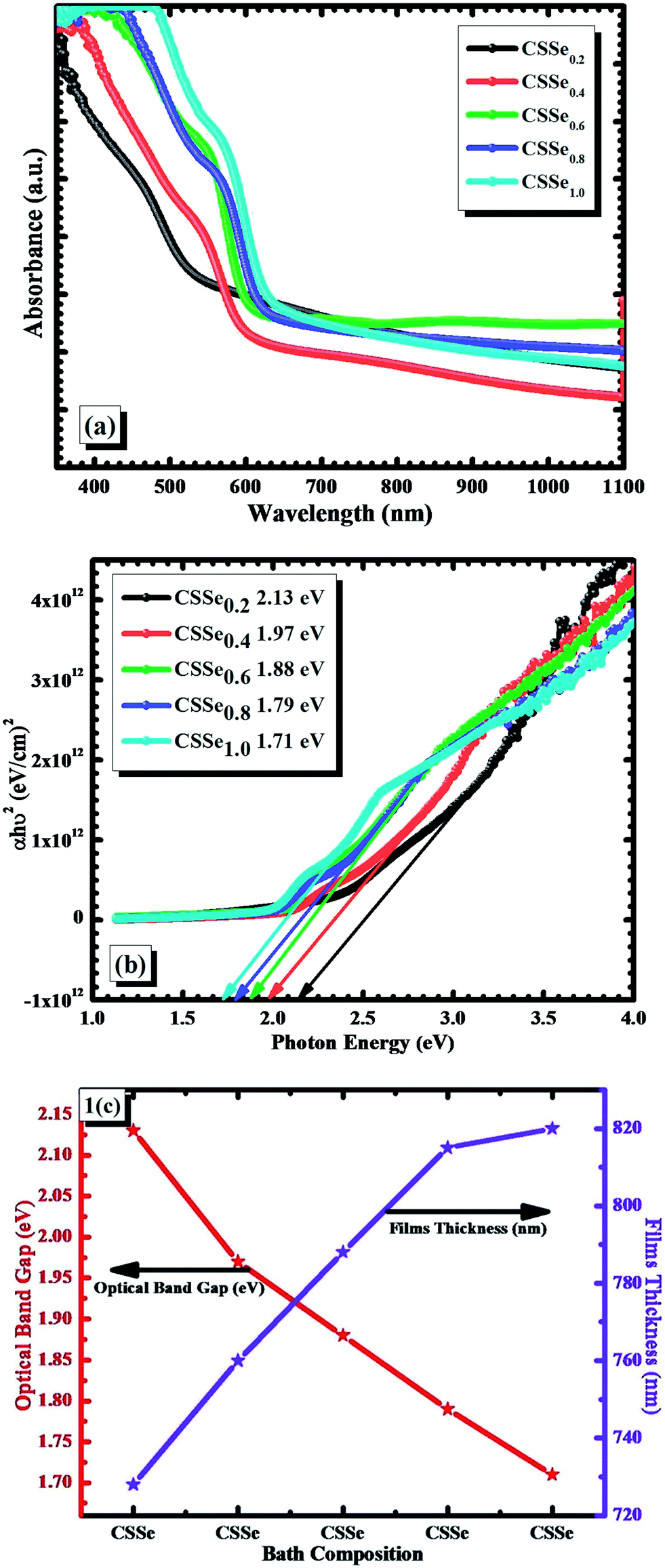
The optical absorption spectra of deposited thin films were recorded in a wavelength range of 350–1100 nm as shown in Fig. 1(a). The absorption coefficients for all samples were found to be on the order of 106 cm−1. Red shifts in the absorption spectra confirm the effective deposition of all samples with enhancement in crystallinity.33 Fundamental absorption, which corresponds to electron excitation from a valance band to conduction band, can be used to determine the optical band gap energy. Optical data were processed by using the following eqn (1),33| |
 | (1) |
where ‘A’ is a parameter that depends on transition probability, h is Planck's constant, ‘Eg’ is the optical band gap energy of the material, and exponent ‘n’ depends on the type of transition. The values of ‘n’ for direct allowed, indirect allowed, and direct forbidden transition are 1/2, 2, and 3/2, respectively. The optical band gap energy values of deposited thin films were obtained by plotting graphs of (αhν)2 vs. photon energy (hν), as shown in Fig. 1(b).
 |
| | Fig. 1 (a) Optical absorption spectra of Cd(S1−xSex) thin films. (b) Plots of (αhν2) (eV cm−1)2 vs. photon energy (hν, eV). (c) Plot of optical band gap energy and film thickness as a function of bath composition. | |
The linear nature of the plots suggest the direct allowed type of transition. The optical band gap energy was obtained by extrapolating the straight line portion of the graph of (αhν)2 vs. photon energy (hν) at α = 0 to the energy axis from 2.13–1.71 eV with varying bath composition, which is summarized in Table 2. Such a modification of the optical band gap energy is due to the quantum confinement effect.40 Generally, for semiconducting materials, electronic excitation occurs through loosely bound electron–hole pairs that delocalize over a length much longer than the lattice constant.40 The quantum confinement effect was recently discussed in detail by the authors.40
Table 2 Thickness, optical band gap (Eg), crystallite size (D), dislocation density (δ) and micro-strain (ε) data of all thin films
| Samples code |
Thickness (nm) |
Band gap (eV) |
Crystallite size (nm) |
Dislocation density (δ) 10−4 (lines m−2) |
Micro-strain (ε) 10−4 (lines−2 m−4) |
| CSSe0.2 |
728 |
2.13 |
55 |
3.3 |
6.4 |
| CSSe0.4 |
760 |
1.97 |
63 |
2.5 |
5.9 |
| CSSe0.6 |
788 |
1.88 |
71 |
1.9 |
5.1 |
| CSSe0.8 |
815 |
1.79 |
79 |
1.6 |
4.5 |
| CSSe1.0 |
820 |
1.71 |
82 |
1.4 |
3.8 |
3.3 Thickness measurement
The thickness of deposited thin films was assessed from 728 to 820 nm with varying bath composition. All thickness values are summarized in Table 2. It was observed that the thickness increases with varying bath composition and the formation of more compact, well adherent films over entire substrate surface. Generally, the slow release of ions from bound complexes results in the formation of compact and good quality thin films. Generally, a decrease in the required amounts of metal and chalcogen ions in the bath solution (2.30 h) causes the thickness to remain constant. Generally, decrement in the required amounts of metal and chalcogen ions in the bath solution causes termination of reaction process. Therefore after this (2.30 h in the present case) reaction time, the thickness of sample remains constant.33 Fig. 1(c) shows that plot of optical band gap energy and films thickness as function of bath composition.
Fig. 1(c) clearly reveals that as the bath composition increases from CSSe0.2 to CSSe1.0 the films thickness increases and the optical band gap energy decreases.
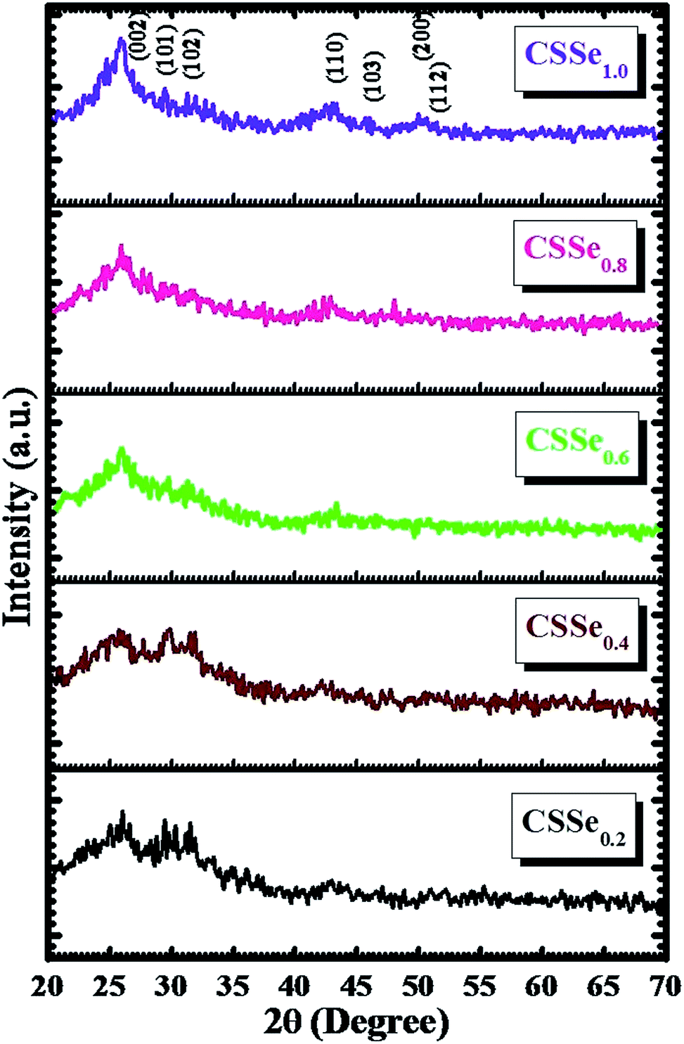
3.4 X-ray diffraction studies
The phase formation and crystallite size of deposited thin films have been studied by using X-ray diffraction (XRD) patterns. Fig. 2 shows XRD patterns of Cd(S1−xSex) thin films at the 20–70° 2θ range. The XRD patterns clearly show that all diffraction peaks are broad and sharp, confirming the nanocrystalline nature of the deposited thin films41 (Fig. 2). Seven diffraction peaks correspond to (002), (101), (102), (110), (103), (200) and (112) at 2θ 26.02°, 28.40°, 31.13°, 42.80°, 44.93°, 50.89° and 52.07° of the pure hexagonal crystal structure. All diffraction peak positions are consistent with other reported data,42,43 confirming the formation of a pure phase material. The observed d-values are in good agreement with standard d-values from the JCPDS data card (49-1459) (Table 3). No other impurity peaks are observed in any of the XRD patterns. Also, the highest intense peaks of the (002) plane slightly shifted towards larger 2θ values with increasing ‘x’ (x = 0.2–1.0) composition. This confirms the formation of pure phase thin films of IIA–VIB group semiconductor materials.42,43 This slight shifting of diffraction peaks indicates that ‘Se’ ions are effectively incorporated into the ternary system.42
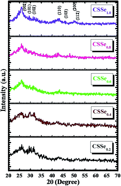 |
| | Fig. 2 X-ray diffraction patterns of deposited Cd(S1−xSex) thin films. | |
Table 3 X-ray diffraction parameters of synthesized thin films
| Sr. no. |
2θ |
(hkl) |
dJCPDS (Å) |
dExp. (Å) |
| 1 |
26.02 |
(002) |
3.389 |
3.420 |
| 2 |
28.40 |
(101) |
3.185 |
3.142 |
| 3 |
31.13 |
(102) |
2.470 |
2.501 |
| 4 |
42.80 |
(110) |
2.088 |
2.110 |
| 5 |
44.93 |
(103) |
1.920 |
2.005 |
| 6 |
50.89 |
(200) |
1.809 |
1.792 |
| 7 |
52.09 |
(112) |
1.780 |
1.754 |
Crystallite size (D) is calculated by using the well-known Scherrer formula.33 Crystallite size was found to range from 55 to 82 nm (Table 2).
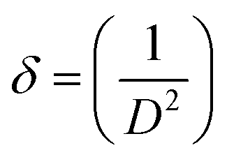
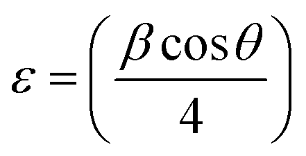
These improved crystallite sizes are beneficial for enhancement of photoconversion efficiency due to lower interfacial energy.44,45 From the calculated crystallite size, the dislocation density (δ) and micro-strain (ε) for all thin films were calculated by using eqn (2) and (3),
| |
 | (2) |
| |
 | (3) |
where
D is crystallite size,
β is the full-width-at-half-maximum (FWHM) in radian, and
θ is Bragg's angle.
The values of δ and ε for all thin films are tabulated in Table 2. Table 2 clearly indicates a decrease in values of δ and ε with varying bath composition. Thus, this decrease in values confirm a lower level of lattice imperfections and the formation of good quality thin films.33,34 Such a lower level of lattice imperfection and the formation of pure material with good quality are beneficial for photoelectrochemical application.33
3.5 High-resolution transmission electron microscopy (HRTEM)
HRTEM and SAED pattern analysis was carried out as a detailed study of crystallinity and to gain more insight into the micro-structures of deposited thin film.40 Fig. 3 displays the transmission electron microscopy (TEM), high-resolution transmission electron microscopy (HRTEM) and selected area electron diffraction (SAED) pattern results for Cd(S0.2Se0.8) thin films. Fig. 3(a and b) shows clear distinct TEM images. It shows formation of a custard apple-like surface morphology through the assembly and aggregation of smaller nanospheres over all of the surface. Such nanospheres form a compact and well covered surface containing a large number of custard apple-like structures. These TEM images match well with obtained FESEM micrographs.
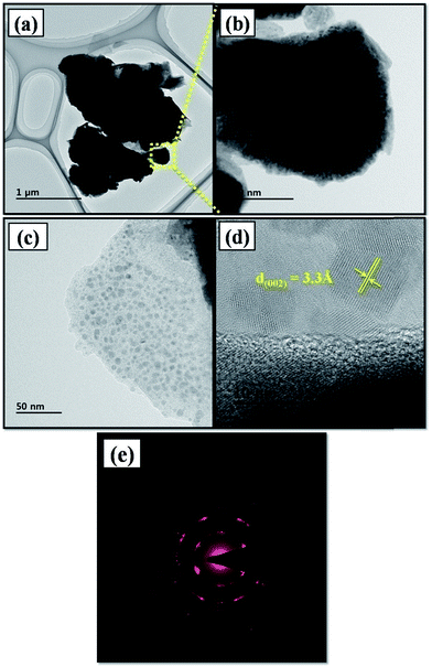 |
| | Fig. 3 (a and b) Transmission electron microscopy images, (c and d) high-resolution transmission electron microscopy images and (e) selected area electron diffraction pattern of Cd(S0.2Se0.8) thin film. | |
HRTEM images at different magnifications are shown in Fig. 3(c and d). The HRTEM image of Fig. 3(c) indicates that nanospheres grew more compact and well-interconnected to each other to form a custard apple-like morphology. Fig. 3(d) demonstrates the good crystallinity of the sample and the lattice fringe of d(002) = 0.33 Å. Such an observed lattice fringe is well consistent with the XRD results.
Furthermore, the SAED pattern in Fig. 3(e) consists of a clearly distinct ring pattern, which confirms the nanocrystalline nature of the deposited thin film.40 The SAED pattern-indicated nanocrystalline nature is in accordance with the results of the XRD study. Overall, the TEM, HRTEM and SAED pattern observations matched well with the obtained XRD and FESEM analysis results.
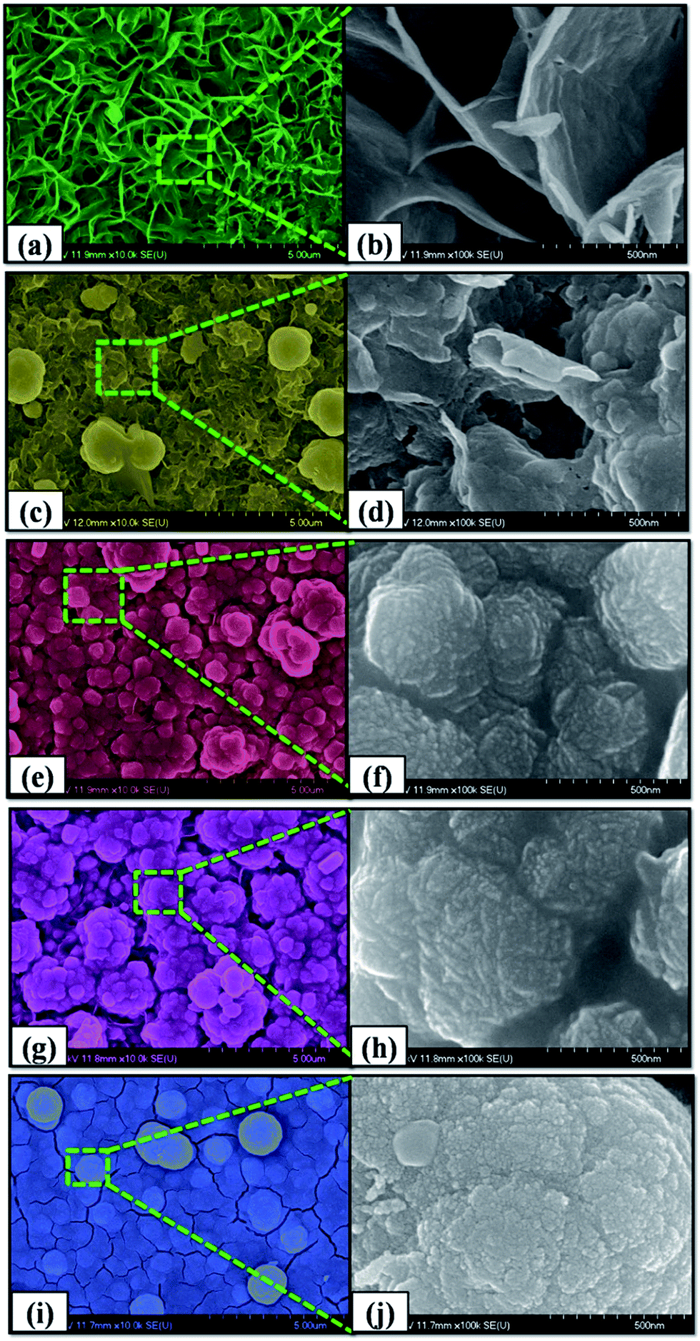
3.6 Surface morphology study
The surface morphology of all thin films was characterized by using FESEM analysis. Fig. 4 shows low and high resolution FESEM images of deposited Cd(S1−xSex) thin films with x = 0.2, 0.4, 0.6, 0.8 and 1.0, respectively. All FESEM images clearly confirm the uniformity of the thin films throughout the substrate surface with well-adherent and clearly defined grains. Fig. 3(a and b) (Cd(S0.8Se0.2)) clearly demonstrates that a nest-like surface morphology is obtained. Such morphology was formed by a large number of densely grown nanowalls over the entire substrate surface interconnected to each other to form a nest-like surface morphology. With a further increase in selenium content (Cd(S0.6Se0.4)), such nest-like morphology is twisted and aggregated to form a compact nest-like surface morphology (Fig. 4(c)). The high-resolution image in Fig. 4(d) clearly shows more aggregation and twisting of the nest over the entire surface and the development of a compact nest-like surface morphology. The low-resolution FESEM image in Fig. 4(e) indicates that with an increase in selenium content (Cd(S0.4Se0.6)), the nest-like surface morphology was disturbed and a nanospherical surface morphology was formed. Fig. 4(f) confirms that smaller nanoparticles are interconnected with aggregation to form this nanospherical morphology on the substrate surface.
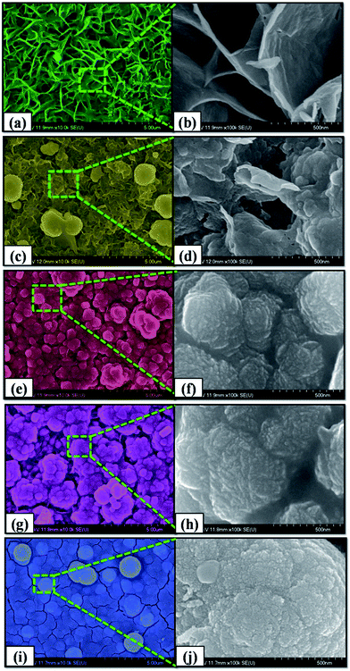 |
| | Fig. 4 Field emission scanning electron microscopy (FESEM) micrographs of Cd(S1−xSex) (x = 0.2–1.0) thin films. | |
The Cd(S0.2Se0.8) thin film in Fig. 4(g) shows the development of the custard apple-like surface morphology. Such morphology is formed by consistent aggregation of nanospheres, which is clearly seen in the high-resolution FESEM image in Fig. 4(h). The assembling number of such small nanospheres to each other results in formation of a single custard apple-like morphology. Such a custard apple-like surface morphology has a large surface area for effectual light absorption.46 Therefore, such a custard apple-like morphology is suitable for photoelectrochemical applications.33,46
Fig. 4(i and j) show low- and high-resolution FESEM images of the Cd(S0.0Se1.0) thin film. The low-resolution FESEM image shows large aggregation and more compactness of the custard apple-like morphology. The high-resolution FESEM image in Fig. 4(j) indicates that a homogeneous bead-like surface morphology is obtained due to more aggregation. The beaded surface morphology contains a type of trough on the upper surface area. These troughs might be due to compact aggregation, faster growth and effective deposition over the entire substrate surface.46 Comparatively, such a homogenous beaded surface morphology containing these troughs, which have a low surface area for light absorption and effective scattering, shows a decrease in the power conversion efficiency.33,46 Overall, the surface analysis study indicates that the obtained surface morphology is promising for effective light absorption for photoelectrochemical application. Such a developed novel surface morphology (custard apple-like) may be suitable for effective light absorption over a large surface area.
3.7 Compositional analysis
X-ray photoelectron spectroscopy (XPS). XPS analysis was performed to determine the chemical state and composition of the Cd(S0.2Se0.8) thin film. Fig. 5(a) shows a survey spectrum of the Cd(S0.2Se0.8) thin film, which clearly shows the presence of cadmium (Cd), sulphur (S), selenium (Se), carbon (C) and oxygen (O) elements in the deposited thin film. The binding energies recorded in the XPS analysis were corrected to take into account specimen charging, setting C1s to 285.02 eV. The presence of a small amount of oxygen in the deposited thin film might be due to extrinsic contamination such as CO2, O2 and H2O on the film surface from atmospheric contamination.34 From the spin–orbital coupling interaction in Cd(3d), two distinct core level spectrums are separated as Cd3d5/2 at a binding energy of 404.78 eV and Cd3d3/2 at a binding energy of 411.67 eV (Fig. 5(b)). The high-resolution core level spectrum of S(2p) in Fig. 5(c) shows a single peak for S(2p) at a binding energy of 160.01 eV. Fig. 5(d) shows the high-resolution core level spectrum for Se(3d). The Se(3d) spectrum shows a single peak at a binding energy of 53.61 eV. All of the observed binding energies at their respective state confirm that Cd2+, S2− and Se2− ions are present in the deposited thin film.33
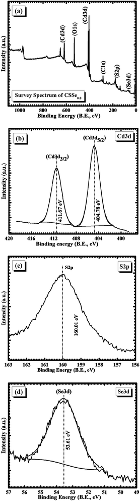 |
| | Fig. 5 (a) XPS survey spectrum of the Cd(S0.2Se0.8) thin film, (b) high-resolution core level XPS spectrum of Cd, (c) high-resolution core level XPS spectrum of S, and (d) high-resolution core level XPS spectrum of Se. | |
Energy dispersive X-ray spectroscopy (EDS). EDS analysis was carried out to determine the presence of elements and the stoichiometric ratio of elements in the deposited thin film. Fig. 6 shows the EDS spectrum of deposited Cd(S0.2Se0.8) thin film. The inset table in Fig. 6 provides tabulated data for the theoretical and actual atomic percentages of Cd, S and Se elements. Fig. 6 shows peaks at 3.13, 2.50 and 1.38 keV, confirming the presence of Cd, S and Se elements, respectively, in the Cd(S0.2Se0.8) thin film. Also, the inset table in Fig. 6 shows a small amount of deviation between the actual atomic percentage from theoretical atomic percentage. Such deviation in the atomic percentage could be due to the absorption and inclusion of oxygen (O) in the film from atmospheric contamination and during transfer of the film.33,47,48 Overall, the EDS analysis study confirms that the actual atomic percentages are in good agreement with theoretical atomic percentages of respective elements.
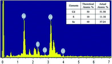 |
| | Fig. 6 EDS pattern of Cd(S0.2Se0.8) thin film, inset table: theoretical and actual atomic percentages of Cd, S and Se elements. | |
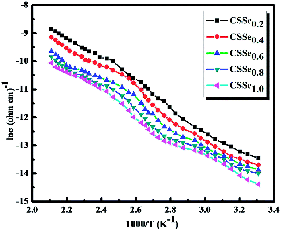
3.8 Electrical studies
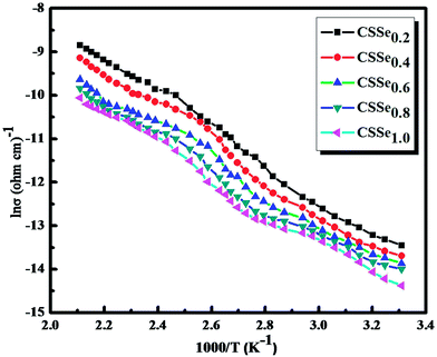
Electrical conductivity (EC) study. Conductivity is essential to study the electrical transport properties of synthesized materials. Fig. 7 shows plot of ln![[thin space (1/6-em)]](https://www.rsc.org/images/entities/char_2009.gif) σ vs. 1000/T for Cd(S1−xSex) thin films. From the graph, it is observed that the conductivity increases correspondingly for all samples, which indicates the semiconducting behavior of Cd(S1−xSex) thin films. The activation energy was estimated by using eqn (4) as follows,where σ is the conductivity of the sample, σ0 is the temperature independent part of the conductivity, Ea is the activation energy, k is the Boltzmann constant, and T is the temperature in Kelvin. A decrease in activation energy with varying bath composition indicates the semiconducting nature of the deposited thin films.34 Table 4 summarizes the values of activation energy for all samples.
σ vs. 1000/T for Cd(S1−xSex) thin films. From the graph, it is observed that the conductivity increases correspondingly for all samples, which indicates the semiconducting behavior of Cd(S1−xSex) thin films. The activation energy was estimated by using eqn (4) as follows,where σ is the conductivity of the sample, σ0 is the temperature independent part of the conductivity, Ea is the activation energy, k is the Boltzmann constant, and T is the temperature in Kelvin. A decrease in activation energy with varying bath composition indicates the semiconducting nature of the deposited thin films.34 Table 4 summarizes the values of activation energy for all samples.
 |
| | Fig. 7 Electrical conductivity (EC) measurement plots for Cd(S1−xSex) (x = 0.2–1.0) thin films. | |
Table 4 Electrical properties of Cd(S1−xSex) thin films
| Sr. no. |
Sample code |
Activation energy 10−3 (Ea, eV) |
Carrier concentration 1019 (cm−3) |
Mobility 10−7 (cm−2 V−1 S−1) |
| 1 |
CSSe0.2 |
0.056 |
3.410 |
12.904 |
| 2 |
CSSe0.4 |
0.054 |
3.452 |
7.115 |
| 3 |
CSSe0.6 |
0.049 |
3.477 |
4.883 |
| 4 |
CSSe0.8 |
0.045 |
3.539 |
4.552 |
| 5 |
CSSe1.0 |
0.044 |
3.557 |
4.417 |
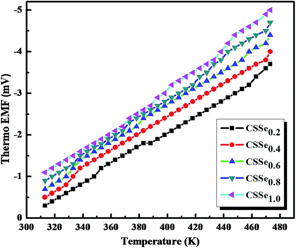
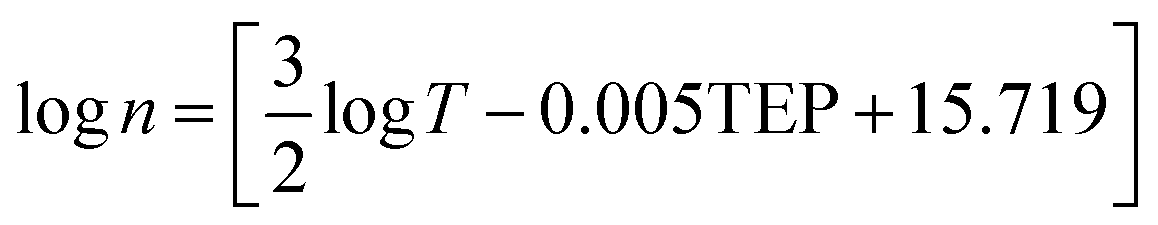
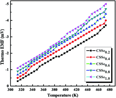
Thermoelectric power (TEP) measurement study. TEP measurements are used to assess differences between thermally generated voltage and the temperature differences across hot and cold ends of semiconducting materials.33,49 The negative polarity of thermo emf indicates that Cd(S1−xSex) thin films are n-type semiconductors.49,50 The plot of thermo emf (mV) vs. temperature (K) for Cd(S1−xSex) thin films is shown in Fig. 8.
 |
| | Fig. 8 Thermoelectric power measurement (TEP) plots of Cd(S1−xSex) (x = 0.2–1.0) thin films. | |
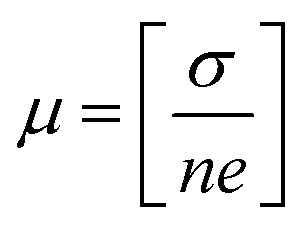
The carrier concentration and mobility for all samples were calculated by eqn (5) and (6) as follows,
| |
 | (5) |
| |
 | (6) |
where
μ is the mobility,
n is the carrier concentration, and
e is the electronic charge. The carrier concentration increased exponentially and mobility decreased with varying bath composition in the deposited thin films due to low values of anti-structural defects in the deposited thin films.
50 The carrier concentration and mobility are specified in
Table 4.
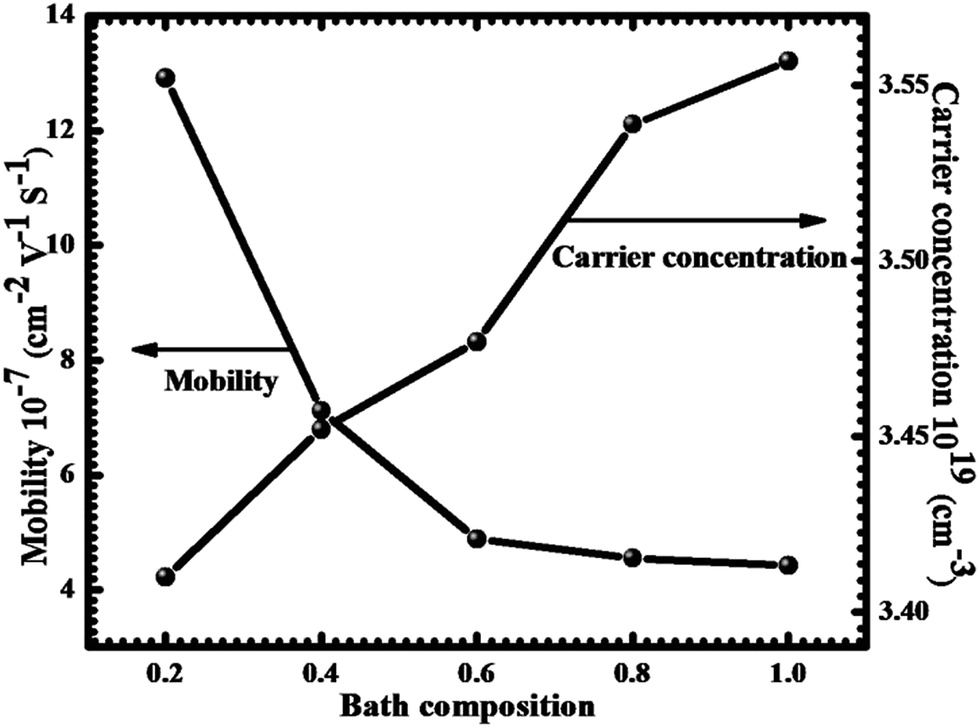
Fig. 9 shows a plot of carrier concentration and mobility as a function of bath composition. It is observed that as the bath composition increases, the carrier concentration increases, which affects the mobility of charge carriers.
 |
| | Fig. 9 Plots of mobility and carrier concentration as a function of varying bath composition. | |
3.9 Photoelectrochemical (PEC) properties
PEC solar cells convert solar energy into electrical energy. PEC solar cells have gained extensive application due to easy junction formation, simple handling and cost effective fabrication.51 They are based on the formation of a junction between a photoelectrode and a suitable redox electrolyte solution. Actually, the electrolyte plays a vital role in solar cells for charge transfer through the photoelectrode and counter electrode.50
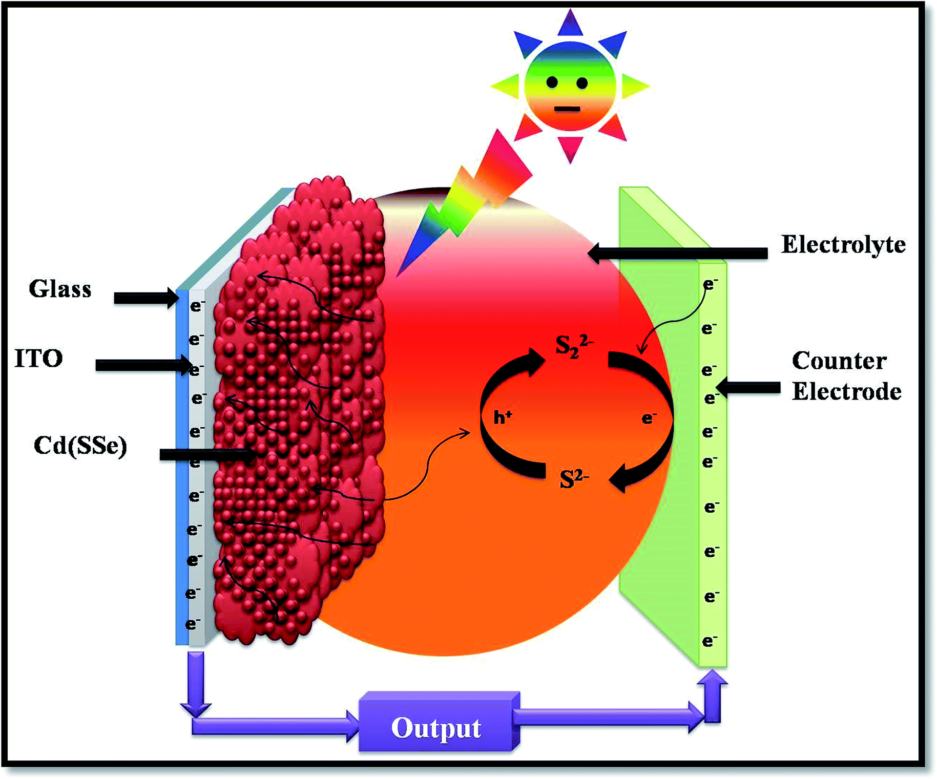
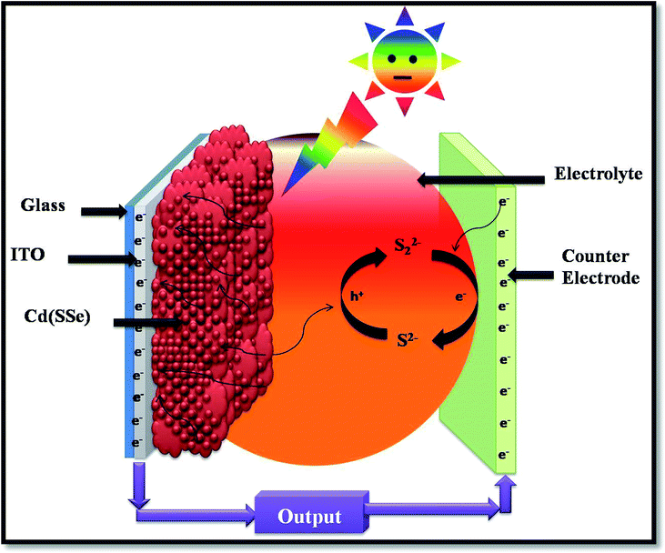
The working principle of PEC solar cells can be methodically related to the electrochemical behavior of the photoactive electrode. It consists of electronically excited charge carriers through irradiation by light in the presence of a suitable redox electrolyte.52 In general, upon illumination, absorption of photons by an active semiconductor photoelectrode causes promotion of electrons from the valence band to conduction band. This results into electron–hole pair formation in the excited state region. After this fast separation of two charge carriers occurs, electrons (majority carrier) are forced towards the inner region of the semiconductor and holes (minority carrier) towards the electrolyte interface.53 With a suitable redox electrolyte, the holes cause oxidation of the reduced species of the redox couple. Separated electrons are collected in the back contact of an active semiconductor (ITO) and transferred towards the counter electrode (graphite) through an external circuit. Further, the oxidized species get reduced to complete this reaction.54 This overall working principle for photoelectrochemical solar cells is schematically illustrated in Scheme 2.
 |
| | Scheme 2 Schematic illustration of the PEC cell working process of a Cd(S1−xSex) thin film photoelectrode deposited via the APT method. | |
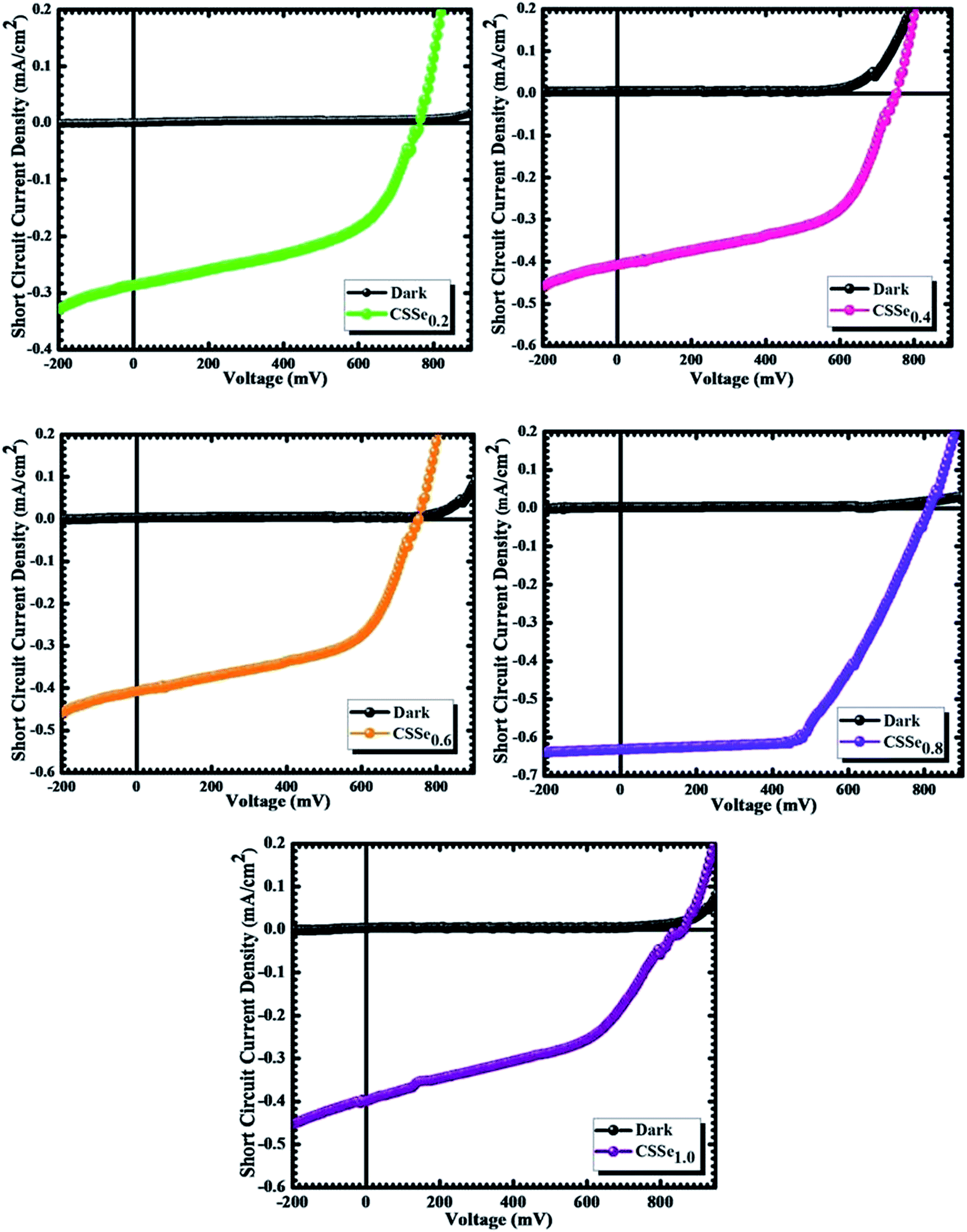
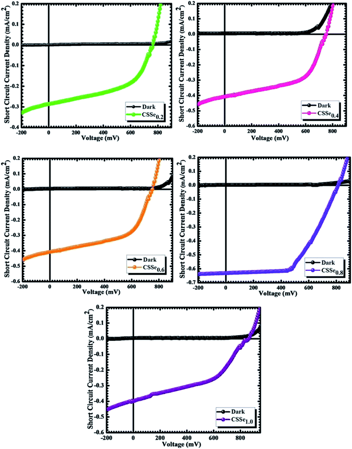
The PEC performance of all deposited thin films was measured with a standard two electrode configuration. Fig. 10 show J–V curves of PEC cells formed with Cd(S1−xSex) thin films as the working electrode and a graphite rod (G) as the counter electrode. J–V measurements were done under illumination of light using a 500 W tungsten filament lamp (intensity of 30 mW cm−2) in 0.5 M sulfide/polysulfide redox electrolyte. In the dark, J–V characteristics show a diode-like rectifying behavior. Upon illumination, the curves are shifted to the fourth quadrant, indicating the generation of a photocurrent, which is a typical PEC characteristic.33 Also, for all samples, the increase in the magnitude of the photocurrent by way of the negative polarity region demonstrates that the material is n-type semiconductor,34,55 which is in agreement with the TEP results. The photoresponses of all samples were assessed by forming the following cell configuration, glass-ITO/Cd(S1−xSex)/polysulfide electrolyte, (Na2S–NaOH–S)aq./G.
 |
| | Fig. 10 J–V plots of Cd(S1−xSex) (x = 0.2–1.0) thin films. | |
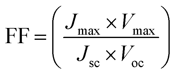
The output parameters of the PEC cell, such as the fill factor (FF) and conversion efficiency (η%), were calculated using relations (7) and (8) as follows,34
| |
 | (7) |
| |
 | (8) |
where
Jmax and
Vmax are the maximum short circuit current density and maximum voltage, respectively,
Pin is the input light intensity (30 mW cm
−2),
Jsc is the short circuit current density, and
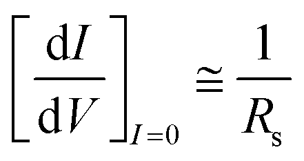
Voc is the open circuit voltage. The values of series resistance (
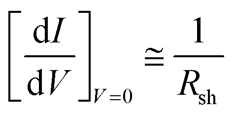
Rs) and shunt resistance (
Rsh) for all samples were calculated from the slope of the power output characteristics using
eqn (9) and
(10),
| |
 | (9) |
| |
 | (10) |
Rs decreased from 1217 Ω to 347 Ω from samples CSSe0.2 to CSSe1.0 respectively. At the same time, the shunt resistance for sample CSSe1.0 (Rsh) is 12430 Ω, and that of sample CSSe0.2 is 5200 Ω. Rs is based on the resistance of metal contact, ohmic contact and junction depth, and Rsh is due to crystal defects. Ideally, Rs and Rsh should be 0 Ω and infinity, respectively.33 Rs, Rsh, and FF respective to the conversion efficiency (η%) of all samples are tabulated in Table 5.
Table 5 Solar cell parameters of Cd(S1−xSex) thin films
| Code |
Eg (eV) |
Jsc (mA cm−2) |
Voc (mV) |
Jmax (mA cm−2) |
Vmax (mV) |
Rs (Ω) |
Rsh (Ω) |
FF |
η (%) |
| CSSe0.2 |
2.13 |
0.288 |
765 |
0.184 |
603 |
1217 |
5200 |
0.50 |
0.37 |
| CSSe0.4 |
1.97 |
0.409 |
767 |
0.299 |
560 |
1184 |
5437 |
0.51 |
0.55 |
| CSSe0.6 |
1.88 |
0.410 |
754 |
0.360 |
518 |
580 |
5625 |
0.60 |
0.61 |
| CSSe0.8 |
1.79 |
0.630 |
810 |
0.544 |
554 |
343 |
6221 |
0.60 |
1.02 |
| CSSe1.0 |
1.71 |
0.415 |
863 |
0.260 |
579 |
1355 |
4946 |
0.42 |
0.50 |
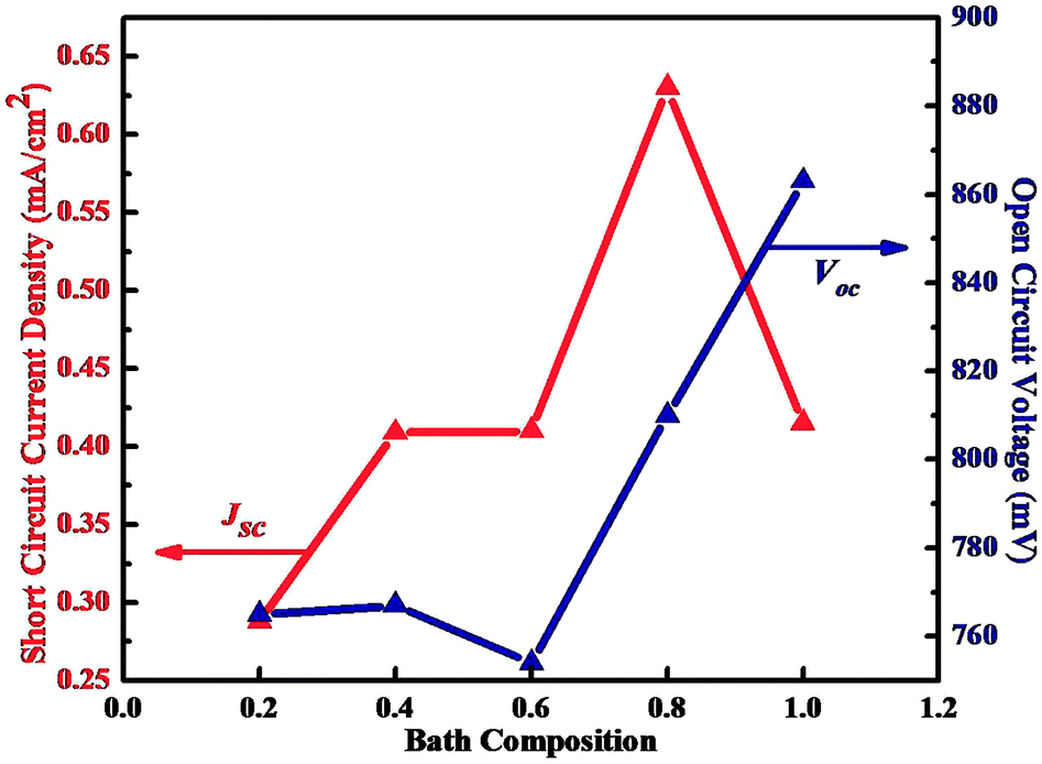
From J–V measurements, the obtained values of Jsc for samples CSSe0.2, CSSe0.4, CSSe0.6, CSSe0.8 and CSSe1.0 were 0.288, 0.409, 0.410, 0.630 and 0.415 mA cm−2 and the corresponding values of Voc were 765, 767, 754, 810 and 863 mV, respectively. The highest conversion efficiency obtained was 1.02% for sample CSSe0.8.
Fig. 11 shows plots of the short circuit current density (JSC) and open circuit voltage (Voc) as a function of bath composition. Fig. 11 demonstrates that the short circuit current density and open circuit voltage are co-related to each other in photoelectrochemical application. It is observed that the values of Jsc and Voc are highest for sample CSSe0.8, which can be attributed to the custard apple-like surface morphology that provides a high surface area and maximum light scattering pathway.40 Fig. 12 shows plots of the conversion efficiency (η%) and fill factor (FF%) as a function of bath composition. The data in Fig. 12 noticeably confirm that varying bath composition and fill factor play imperative roles in achieving an enhanced power conversion efficiency. Such factors are extremely reliant on different preparative parameters of high-efficiency thin films.
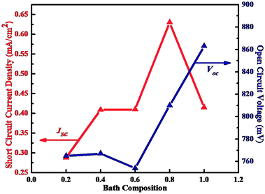 |
| | Fig. 11 Current density (JSC) and open circuit voltage (Voc) as a function of varying bath composition. | |
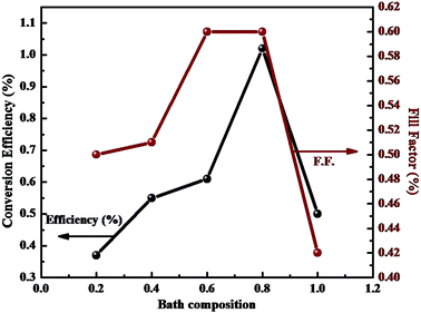 |
| | Fig. 12 Conversion efficiency (%) and fill factor as a function of varying bath composition. | |
From a literature survey on Cd(S1−xSex) thin films, the obtained 1.02% power conversion efficiency is highest. These results are considerably better than those for Cd(SSe) thin films deposited by sophisticated techniques.
4. Conclusions
We have successfully deposited Cd(S1−xSex) thin films using a self-organized hybrid aqueous chemical method. The developed distinctive morphology demonstrated the highest power conversion efficiency (1.02%) reported to date. The observed structural, morphological and electronic properties indicate that Cd(S1−xSex) thin films have great potential for solar cell application. Maximum light absorption is observed in the visible region of the solar spectrum over the 620–750 nm wavelength range. The absorption coefficients for all samples were found to be on the order of 106 cm−1, and the linear nature of absorption plots confirm the direct allowed type of transition. The thickness of deposited thin films increases from 728–820 nm and the band gap energy decreases from 2.13–1.71 eV with varying bath composition. The XRD patterns confirm the formation of pure phase films. The crystallite size was found to be in the range of 55–82 nm with a decrease in the dislocation density and micro-strain of the deposited thin films. HRTEM images illustrated that a compact and crystalline thin film was deposited on the substrate surface. The SAED pattern confirmed the nanocrystalline nature of the thin film. FESEM micrographs highlighted effective, homogenous and well-adherent deposition over all of the substrate surface. XPS analysis indicated binding energies for Cd2+, S2− and Se2− elements that are in their respective positions. The formation of thin films in a stoichiometric ratio was confirmed by EDS analysis. EC measurements showed that the deposited films are semiconducting in nature. The n-type conductivity was verified by TEP analysis. J–V measurements showed that the highest conversion efficiency is 1.02% for the custard apple-like Cd(S0.2Se0.8) thin film. Such a high conversion efficiency might be due to the large surface area and improved crystallinity with lower values of dislocation density and micro-strain.
Overall, the observed results reveal that deposition of Cd(S1−xSex) thin films using hybrid technique is constructive for the invention of new mixed metal chalcogenide-based thin films, particularly for solar cell application.
Acknowledgements
One of the authors, Mr Kishorkumar V. Khot, is very much thankful to the Department of Science and Technology (DST), New Delhi for providing DST-INSPIRE fellowship for financial support (Registration no. IF130751). This research was supported by the Basic Science Research Program through the National Research Foundation of Korea (NRF) funded by the Ministry of Education (NRF-2009-0094055) and NRF-2014R1A2054051
Notes and references
- M. R. Gao, Y. F. Xu and S. H. Yu, Chem. Soc. Rev., 2013, 42, 2986 RSC.
- M. Winter and R. J. Brodd, Chem. Rev., 2004, 104, 4245 CrossRef CAS.
- A. S. AricO, P. Bruce, B. Scrosati, J. M. Tarascon and W. V. Schalkwijk, Nat. Mater., 2005, 4, 366 CrossRef CAS PubMed.
- A. Kudo and Y. Miseki, Chem. Soc. Rev., 2009, 38, 253 RSC.
- Y. J. Wang, D. P. Wilkinson and J. J. Zhang, Chem. Rev., 2011, 111, 7625 CrossRef CAS PubMed.
- R. R. Adzic, J. Zhang, K. Sasaki, M. B. Vukmirovic, M. Shao, J. X. Wang, A. U. Nilekar, M. Marvikakis, J. A. Valerio and F. Uribe, Top. Catal., 2007, 46, 249 CrossRef CAS.
- S. E. Habas, H. A. S. Platt, F. A. M. Van Hest and D. S. Ginley, Chem. Rev., 2010, 110, 6571 CrossRef CAS PubMed.
- M. G. Walter, E. L. Warren, J. R. Mckone, S. W. Boettcher, Q. X. Mi, E. A. Santori and N. S. Lewis, Chem. Rev., 2010, 110, 6446 CrossRef CAS PubMed.
- P. Simon and Y. Gogotsi, Nat. Mater., 2008, 7, 845 CrossRef CAS PubMed.
- C. Burda, X. B. Chen, R. Narayanan and M. A. EI-Sayed, Chem. Rev., 2005, 105, 1025 CrossRef CAS PubMed.
- C. H. Lai, M. Y. Lu and L. J. Chen, J. Mater. Chem., 2012, 22, 19 RSC.
- C. N. R. Rao, G. U. Kulkarni, P. J. Thomas and P. P. Edwards, Chem.–Eur. J., 2000, 8, 29 Search PubMed.
- P. V. Kamat, J. Phys. Chem. C, 2007, 111, 2834 CAS.
- P. V. Kamat, K. Tvrdy, D. R. Baker and J. G. Radich, Chem. Rev., 2010, 110, 6664 CrossRef CAS PubMed.
- T. Otto, M. Müller, P. Mundra, V. Lesnyak, H. Demir, V. N. Gaponik and A. Eychmüller, Nano Lett., 2012, 12, 5348–5354 CrossRef CAS PubMed.
- B. O. Dabbousi, M. G. Bawendi, O. Onitsuka and M. F. Rubner, Appl. Phys. Lett., 1995, 66, 1316 CrossRef CAS PubMed.
- V. Kumar, S. K. Sharma and D. K. Dwivedi, J. Alloys Compd., 2012, 512, 351 CrossRef CAS PubMed.
- T. Gruszecki and B. Holmstorm, Sol. Energy Mater. Sol. Cells, 1993, 31, 227 CrossRef CAS.
- J. Heo, H. Ahn, R. Lee, Y. Han and D. Kim, Sol. Energy Mater. Sol. Cells, 2003, 75, 193 CrossRef CAS.
- C. J. Hibberd, K. Ernits, M. Kaelin, U. Muller and A. N. Tiwari, Prog. Photovoltaics, 2008, 16, 585 CAS.
- A. A. Yadav and E. U. Masumdar, Sol. Energy, 2010, 84, 1445 CrossRef CAS PubMed.
- M. Hussain, B. P. Singh, S. Kumar, T. P. Sharma and P. J. Sebastian, Sol. Energy Mater. Sol. Cells, 2003, 76, 399 CrossRef.
- R. S. Mane and C. D. Lokhande, Thin Solid Films, 1997, 304, 56 CrossRef CAS.
- D. Bhattacharya, S. Mohanty and S. N. Sahu, Proceedings of Solid State Physics Symposium, 36-C, BARC, Bombay, 1993, vol. 537, p. 27 Search PubMed.
- F. Y. Siddiqui, S. U. Shaikh, D. J. Desale, D. S. Upadhye, S. V. Mahajan, A. V. Ghule, P. Varshney, S. H. Han and R. Sharma, Mater. Sci. Semicond. Process., 2014, 27, 404 CrossRef CAS PubMed.
- S. R. Gosavi, N. G. Deshpande, Y. G. Gudage and R. Sharma, J. Alloys Compd., 2008, 448, 344 CrossRef CAS PubMed.
- J. C. Blake, P. S. Eldridge and L. Gundlach, Chem. Phys., 2014, 442, 128 CrossRef CAS PubMed.
- M. H. Badwi, S. Aboul-Enein, M. Ghali and G. Hasan, Renewable Energy, 1998, 14, 107 CrossRef.
- H. Fujiyasu, Y. Takeuchi, K. Hikida, K. Masuo, Y. Gotou, T. Kiichi, K. Ishino and A. Ishida, Appl. Surf. Sci., 1993, 65, 455 CrossRef.
- C. D. Lokhande, Mater. Chem. Phys., 1991, 1, 27 Search PubMed.
- S. Bhushan and S. Shrivastava, Opt. Mater., 2006, 28, 1334 CrossRef CAS PubMed.
- T. Chandra and S. Bhushan, J. Mater. Sci., 2004, 39, 6303 CrossRef CAS.
- K. V. Khot, S. S. Mali, N. B. Pawar, R. R. Kharade, R. M. Mane, V. V. Kondalkar, P. B. Patil, P. S. Patil, C. K. Hong, J. H. Kim, J. Heo and P. N. Bhosale, New J. Chem., 2014, 38, 5964 RSC.
- K. V. Khot, S. S. Mali, R. R. Kharade, R. M. Mane, P. S. Patil, C. K. Hong, J. H. Kim, J. Heo and P. N. Bhosale, J. Mater. Sci.: Mater. Electron., 2014, 25, 5606 CrossRef CAS.
- A. E. Tsurkan, T. D. Shemyakova and S. P. Medvetskii, Sol. Energy Mater., 1988, 18, 61 CrossRef CAS.
- A. Pan, H. Yang, R. Yu and B. Zou, Nanotechnology, 2006, 17, 1083 CrossRef CAS PubMed.
- C. Yang, X. Zhou, L. Wang, X. Tian, Y. Wang and Z. Pi, J. Mater. Sci, 2009, 44, 3015 CrossRef CAS PubMed.
- W. Ostwald, Lehrbuch der Allgemeinen Chemie, Leipzig, Germany, 1896, vol. 1, p. 2 Search PubMed.
- R. M. Mane, S. R. Mane, R. R. Kharade and P. N. Bhosale, J. Alloys Compd., 2011, 491, 321 CrossRef PubMed.
- K. V. Khot, S. S. Mali, N. B. Pawar, R. M. Mane, V. V. Kondalkar, V. B. Ghanwat, P. S. Patil, C. K. Hong, J. H. Kim, J. Heo and P. N. Bhosale, J. Mater. Sci.: Mater. Electron., 2014, 25, 3762 CrossRef CAS PubMed.
- M. M. Salunkhe, K. V. Khot, P. S. Patil, T. M. Bhave and P. N. Bhosale, New J. Chem., 2015 10.1039/c4nj01790k.
- S. Muthukumaran and M. Muthusamy, J. Mater. Sci.: Mater. Electron., 2012, 23, 1647 CrossRef CAS PubMed.
- J. B. Chaudhari, N. G. Deshpande, Y. G. Gudage, A. Ghosh, V. B. Huse and R. Sharma, Appl. Surf. Sci., 2008, 254, 6810 CrossRef CAS PubMed.
- S. Min, O. Joo, R. S. Mane, K. Jung, C. D. Lokhande and S. Han, J. Photochem. Photobiol., A, 2007, 187, 133 CrossRef CAS PubMed.
- N. Revathi, R. P. Prathap, R. W. Miles and K. T. R. Reddy, Sol. Energy Mater. Sol. Cells, 2010, 94, 1487 CrossRef CAS PubMed.
- A. I. Inamdar, S. H. Mujawar, V. Ganesan and P. S. Patil, Nanotechnology, 2008, 19, 325706 CrossRef CAS PubMed.
- R. M. Mane, V. B. Ghanwat, V. V. Kondalkar, K. V. Khot, S. R. Mane, P. S. Patil and P. N. Bhosale, Procedia Mater. Sci., 2014, 6, 1285 CrossRef CAS PubMed.
- C. Garza, S. Shaji, A. Arato, E. P. Tijerina, G. A. Castillo, T. K. D. Roy and B. Krishnan, Sol. Energy Mater. Sol. Cells, 2001, 95, 2011 Search PubMed.
- M. M. Salunkhe, N. B. Pawar, K. V. Khot, P. S. Patil, T. M. Bhave and P. N. Bhosale, J. Mater. Sci.: Mater. Electron., 2015, 26, 2921 CrossRef CAS.
- N. B. Pawar, S. S. Mali, S. D. Kharade, M. G. Gang, P. S. Patil, J. H. Kim, C. K. Hong and P. N. Bhosale, Curr. Appl. Phys., 2014, 14, 508 CrossRef PubMed.
- N. L. Tarwal, R. S. Devan, Y. R. Ma, R. S. Patil, M. M. Karanjkar and P. S. Patil, Electrochim. Acta, 2012, 72, 32 CrossRef CAS PubMed.
- J. Poppe, S. G. Hickey and A. Eychmüller, J. Phys. Chem. C, 2014, 118, 17123 CAS.
- S. S. Mali, H. Kim, P. S. Patil and C. K. Hong, Dalton Trans., 2013, 42, 16961 RSC.
- S. S. Mali, H. Kim, C. S. Shim, W. R. Bae, N. L. Tarwal, S. B. Sadale, P. S. Patil, J. H. Kim and C. K. Hong, CrystEngComm, 2013, 15, 5660 RSC.
- R. C. Pawar, J. S. Shaikh, N. L. Tarwal, M. M. Karanjkar and P. S. Patil, J. Mater. Sci.: Mater. Electron., 2012, 23, 349 CrossRef CAS.
Footnote |
| † Electronic supplementary information (ESI) available: The detail information about thin films deposition assembly (APT) and their associated accessories with their respective cross sectional views. See DOI: 10.1039/c4ra16311g |
|
| This journal is © The Royal Society of Chemistry 2015 |
Click here to see how this site uses Cookies. View our privacy policy here.