XANES, EXAFS and photocatalytic investigations on copper oxide nanoparticles and nanocomposites

Aditya Sharma *a, Mayora Varshney a, Jaehun Park a, Tae-Kyun Ha a, Keun-Hwa Chae b and Hyun-Joon Shin *a
aPohang Accelerator Laboratory, POSTECH, Pohang 790-784, South Korea. E-mail: shj001@postech.ac.kr; adityaiuac@gmail.com
bAdvanced Analysis Center, Korea Institute of Science and Technology, Seoul 136-791, South Korea

Received 11th December 2014 , Accepted 16th February 2015

First published on 16th February 2015


Abstract

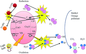
CuO nanoparticles (NPs) and Cu2O/CuO and CuO/TiO2 nanocomposites (NCs) have been synthesized by using a modified co-precipitation method with three different schemes of synthesis. The crystal structures and morphologies of the samples have been investigated using synchrotron X-ray diffraction and transmission electron microscopy, respectively. The detailed local electronic structures of the NPs and NCs have been determined using X-ray absorption near edge structure (XANES) and extended X-ray absorption fine structure (EXAFS) spectroscopy. O K-, Cu K- and Cu L-edge XANES spectra revealed a dominant +2 valence state of Cu in the case of the CuO NPs and CuO/TiO2 NCs, although Cu+1 was dominant in the Cu2O/CuO NCs. A comparison of the local atomic structure around the Cu sites revealed shorter Cu–O bond distances in the as-synthesized samples with respect to the bulk CuO or Cu2O. The Ti K-edge EXAFS fittings for the CuO/TiO2 NCs revealed that the local anatase TiO2 phase was formed, with a Ti–O bond distance of 1.98 Å. We further demonstrated that the CuO NPs, and Cu2O/CuO and CuO/TiO2 NCs can serve as effective photocatalysts towards the degradation of two novel water pollutants, (i) methyl orange (MO) and (ii) potassium dichromate (PD), under visible light irradiation. It was found that the Cu2O/CuO NCs exhibit a higher photocatalytic activity towards the degradation of MO and PD than the CuO NPs or CuO/TiO2 NCs. The mechanism of the photodegradation of MO and PD is also discussed in terms of possible chemical reactions, along with the electronic structure and surface properties of the samples.


1. Introduction

Recently, nanostructures of TiO2, SnO2 and ZnO have been reported for their photocatalytic properties towards the degradation of water pollutants by generating electron–hole pairs under light irradiation.1,2 These metal oxides are known as n-type transparent conducting oxides (TCOs) and have been utilized in gas sensing,3 electrodes for Li ion batteries,4 dye-sensitized solar cells5 and medicinal applications.6 Most of these TCOs have a large energy band gap (>3 eV), which lies in the ultraviolet (UV) range of the solar spectrum. Therefore, it is hard to generate electron–hole pairs from these materials under visible light irradiation. This limits the photocatalytic efficiency of such TCOs under solar light. Hence, there is a thirst to develop new photocatalyst materials with low energy band gaps and high photocatalytic efficiencies under visible light irradiation.

Copper oxides (CuO and Cu2O) are known as important p-type semiconductor materials having direct energy band gaps and unique optical and magnetic properties.7–9 In CuO, the lattice has monoclinic symmetry (m-CuO; space group-C2/c) and each atom of this compound has four nearest neighbors of their kind. The Cu atoms are at the centre of an O rectangle and the O atoms are at the centre of a distorted tetrahedron of Cu.10 The crystallographic structure of Cu2O is highly symmetric (space group-Pn[3 with combining macron]m) with six atoms per unit cell. The O atoms form a body-centered cubic lattice, and the Cu atoms are situated on the vertices of a tetrahedron around each O atom.10 CuO has an open Cu3d configuration (3d9) and is known to be an antiferromagnetic semiconductor with an energy band gap of ∼1.7 eV. However, Cu2O has an essentially full Cu3d shell (3d10) and presents a larger energy band gap ∼2.1 eV.11

Due to the low band gap energy and easy accessibility of copper oxides, there are efforts to degrade water pollutants (methyl orange (MO), potassium dichromate (PD), phenoxazin-3-one, etc.) by using copper oxide as a sensitizer in a composite photocatalyst, such as CuO/ZnO,12 CuO/zeolite,13 CuO/BiVO4[thin space (1/6-em)]14 and CuO/Cu core–shell nanostructures.15 In these studies, the photocatalytic activity was not satisfactory when CuO or Cu2O NPs alone were used as the photocatalyst. Few recent reports are available on the photocatalytic properties of CuO nanostructures with unusual morphologies under UV light irradiation.16–20 The preparation of unusual morphologies requires sophisticated synthesis procedures and high operational temperatures/pressures. Besides this, the Cu metallic phases are also formed in such synthesis methods, which affects the photocatalytic performance of the products.17 Therefore, it is desirable to develop stable catalyst materials with low cost synthesis methods and high efficiencies. It is expected that the catalytic properties of copper oxide may be tailored by modifying its electronic structure (either by adding foreign elements or by making mixed polymorphs).

To understand the role of copper oxide in the catalytic reactions, it is advantageous to establish a relationship between the electronic structure and catalytic activity of compounds. In most of the previous reports, X-ray photoelectron spectroscopy (XPS) has been employed to determine the oxidation state of copper.18–22 Although this technique often provides information regarding the oxidation state of copper in certain thin samples, (i) it is mainly a surface probing technique and (ii) it generally involves cumbersome fitting procedures because the Cu2p XPS peaks of Cu+, Cu+2 and metallic Cu all appear within a very narrow energy range. Therefore, other element specific techniques like X-ray absorption spectroscopy (XAS), within low and high energy ranges, may be favorable for the investigation of the local atomic structure, coordination number, valence state and hybridization of the probed atoms. In this study, we employed a modified co-precipitation synthesis for the preparation of stable CuO NPs and Cu2O/CuO and CuO/TiO2 NCs. Comprehensive electronic structure studies using XAS and photocatalytic investigations suggest that the as prepared materials can serve as effective photocatalysts for the degradation of MO and PD under visible light irradiation.

2. Experimental

2.1 Synthesis of CuO NPs, and CuO/Cu2O and CuO/TiO2 NCs

For the synthesis of the copper oxide photocatalyst materials, we applied a previously established co-precipitation method23,24 with a modified strategy. There were three major synthesis schemes used in the present work: (a) in the first scheme, 5 g of Cu(CH3COO)3·5H2O (Aldrich, 99.9 purity) was mixed into 200 mL of double distilled (DI) water with constant stirring for 45 minutes at room temperature. (b) In the second scheme, 1.5 g of PVA was dissolved into 25 mL DI water and then added, with stirring, into a similar previously prepared Cu(CH3COO)3·5H2O solution. (c) In the third scheme, clear solutions of Cu(CH3COO)3·5H2O and TiCl4·5H2O were prepared according to their molar ratio (10 mol% of Ti was taken with respect to Cu) and then mixed together with stirring. In each scheme of the synthesis, when the chemicals had been fairly dissolved, a diluted NH4OH solution was added drop-wise under constant stirring until the solution reached pH ∼ 9. The brown-blue colored precipitates so formed were washed several times with DI water and then dried at 100 °C in air. The dark brown/blue colored samples were crushed in a mortar–pestle and the finely powdered samples were carefully collected. The samples, synthesized by the different schemes, are named as S1 (CuO NPs), S2 (Cu2O/CuO NCs) and S3 (CuO/TiO2 NCs), respectively. The synthesis schemes, chemicals used, sample names and compositions of the samples are summarised in the Table 1.
Table 1 Summary of synthesis schemes of the samples, sample names, particle sizes calculated using XRD and TEM, and details of the compounds
Preparation method Chemicals/materials used Sample name Particle size (nm) Product detail
XRD TEM
Co-precipitation (Scheme 1) Cu(CH3COO)3·5H2O + DI water + NH4OH S1 8.5 4.8–8.1 CuO
Co-precipitation (Scheme 2) Cu(CH3COO)3·5H2O + DI water + PVA + NH4OH S2 6.2 (Cu2O) 4–6.8 Cu2O + CuO
3.4 (CuO)
Co-precipitation (Scheme 3) Cu(CH3COO)3·5H2O + TiCl4·5H2O + DI water + NH4OH S3 8.2 (CuO) 5.5–8 CuO + TiO2
5.6 (TiO2)


2.2 Photocatalytic experiments

The evaluation of the photocatalytic activities of the as-synthesized samples were performed at room temperature by monitoring the degradation of aqueous solutions of MO and PD. The procedure was as follows: (i) 0.2 g L−1 aqueous solutions of MO and PD were prepared in the dark and stirred for 45 minutes. (ii) 0.1 g of the as-synthesized samples were dispersed into 50 mL of the previously prepared MO and PD aqueous solutions and stirred for 30 minutes in the dark to ensure the adsorption of MO and PD onto the catalyst surface. (iii) A commercial 150 W tungsten-filament bulb was used as a light irradiation source. To avoid thermal effects, the bulb was kept ∼20 inches above the beaker, the beaker was placed on a cold water plate and the water was changed every 15 minutes. (iv) At regular intervals (30 min), 10 mL of the suspensions were sampled and the NPs and NCs were separated by centrifugation for 10 min. (v) Changes in the MO and PD concentrations with irradiation time were monitored by measuring the UV-visible absorption spectra.

2.3 Characterization

The crystal structures and phases of the as-prepared samples were characterized using synchrotron X-ray diffraction (λ = 1.240 Å) performed at an X-ray scattering beam line (3D beam line of Pohang Accelerator laboratory (PAL), South Korea). The morphologies and crystallite sizes were studied using high resolution transmission electron microscopy (HR-TEM) with a JOEL-JEM-2200FS microscope, accompanied with selected area electron diffraction (SAED). To prepare the samples for the HR-TEM measurements, the powder samples were dispersed in an ethanol solution using a sonicator and then the suspended powders were loaded drop-wise on carbon-coated Cu grids. X-ray absorption near edge structure (XANES) spectra at the O K-edge, Cu L-edge and Ti L-edge were collected in the total electron yield (TEY) mode at the 10D (PAL-KIST) beam line. The photon energy resolution of this beam line was better than 0.6 eV (at the O K-edge). The extended X-ray absorption fine structure (EXAFS) measurements at the Cu K-edge and Ti K-edge were performed at the 1D (PAL-KIST) beam line. This beam line utilizes a Si (311) double crystal monochromator and the higher harmonics were effectively removed by detuning the crystals to 70% of the maximum intensity. Ionization chambers, filled with Ar gas, were used to record the intensity of the incident and the transmitted X-rays (the sample is placed between the first and second ionization chamber). The UV-visible absorption spectra of the catalyst samples were collected by using a Varian Cary-100 UV-visible spectrophotometer.

3. Results

3.1 XRD results

Fig. 1 shows the XRD patterns of the as-synthesized samples. All of the XRD spectra were analyzed using the Powder X software. The diffraction patterns of sample S1 fairly resemble the monoclinic phase of CuO (space group-C2/c, lattice parameters: a = 4.689 Å, b = 3.426 Å, c = 5.132 Å, α = γ = 90°, β = 99.653°). The high intensity peak at 2θ = 29.2° and another low intensity peak at 2θ = 33.7° in sample S2 fairly resemble cubic Cu2O (space group-Pn[3 with combining macron]m, lattice parameters: a = b = c = 4.2696 Å, α = β = γ = 90°). However, some other low intensity diffraction peaks at 28.3°, 39.8° and 48.6° match monoclinic CuO. Thus, sample S2 reveals the formation of composite Cu2O/CuO phases. The diffraction peaks of sample S3 fairly match the CuO phase, while the peaks at 25.5° and 31.6° were roughly fitted with either the Ti2O3 rhombohedral phase or the TiO2 anatase phase. Since the rhombohedral Ti2O3 is known to be an unstable phase of titanium oxide, the XRD patterns of sample S3 suggest the formation of copper oxide and titanium oxide composite phases. The average grain size was calculated using the Scherrer relation: D = 0.9λ/β[thin space (1/6-em)]cos[thin space (1/6-em)]θ (D is the grain size, λ is the wavelength of the X-rays used and β is the full width at half maximum of the diffraction peak). The estimated grain sizes of all three samples are tabulated in Table 1.
image file: c4ra16217j-f1.tif
Fig. 1 X-ray diffraction patterns of samples S1 (CuO NPs), S2 (Cu2O/CuO NCs) and S3 (CuO/TiO2 NCs).

3.2 TEM-SAED results

Fig. 2(a)–(c) show the TEM images of samples S1, S2 and S3, respectively. The left and right insets in each image show the size distribution histograms and SAED patterns, respectively. The size distribution of the nanoparticles is tabulated in Table 1. The encircled areas in the TEM images show the closer view of the particles and crystallographic planes. The ring patterns in the SAED images are convincing of the crystalline nature of the samples. However, aggregation of the NPs is visible in all of the TEM images. Such aggregation is expected in the wet chemically synthesized samples due to the marginal presence of hydroxyl groups on the NP surface.23,24
image file: c4ra16217j-f2.tif
Fig. 2 TEM images of (a) sample S1 (CuO NPs), (b) sample S2 (Cu2O/CuO NCs) and (c) sample S3 (CuO/TiO2 NCs) (left and right insets show the histograms of size distribution and SAED patterns, respectively).

3.3 O K-edge XANES

XANES measurements probe the density of states of empty/partially filled electronic states by considering the excitation of an inner shell electron to those states that are allowed by dipole selection rules.25,26 The major feature in the O K-edge spectra of various transition metal oxide compounds can be rationalized using the molecular orbital theory.26 According to this, O K-edge XANES features are the result of the transition of a O1s electron to the various partially occupied and unoccupied molecular orbitals of the oxide, taking into account the crystal-field splitting effects. In the case of cubic or monoclinic type compounds (i.e., CeO2, ZrO2, CuO, Cu2O, etc.) the metal dxy, dxz and dyz orbitals point towards the oxygen atoms, while the dx2y2 and dz2orbitals point between the ligands. As a result, the eg (group of dx2y2 and dz2) orbital is lowered in energy and the t2g orbital (group of dxy, dxz, and dyz) is risen in energy.26 The energy difference between eg and t2g is called the crystal-field splitting parameter and is represented by 10 Dq. Fig. 3 presents the feature-rich O K-edge XANES spectra of the as-synthesized samples. There are four major peaks present in the O K-edge spectra of sample S1 at 531.8 eV, 536.5 eV, 540.6 eV and 545.3 eV. The first peak in the spectrum of sample S1 can be assigned to a 1s → 3eg transition of CuO.27 The 3eg orbital is partially filled because of the d9 configuration of Cu+2 in CuO and is formed by the hybridization of the O2p and Cu3d states.27 The rest of the peaks at higher energies are due to the transitions to the hybridized orbitals of O (2p and 3p) and Cu (4s and 4p).27 The energy separation of the first two peaks (∼4.6 eV) is consistent with previous reports25,27 and supported the formation of the dominant CuO phase in the first synthesis scheme. Interesting variations have been observed in the spectrum of sample S2, with the presence of a peak like feature at ∼534.4 eV (marked by an asterisk). Previous reports have shown that Cu2O exhibits the 1s → eg transition at a higher energy (∼2.7 eV) than that of CuO.27 In the present study, too, this peak is ∼2.6 eV higher in energy over the 1s → 3eg transition peak (at 531.8 eV) of the CuO polymorphs, suggesting the formation of mixed Cu2O and CuO phases in sample S2. The intensity of the first peak (at 531.8 eV) is lower in sample S2, indicating a low concentration of the CuO phase in this sample. Sample S3 also exhibits remarkable changes in its O K-edge features (marked by downward-pointing arrows). Except for the four sharp features of the CuO phase, there are two more features present at 533.2 eV and 537.9 eV. These spectral features did not match with the spectral features of the CuO and Cu2O phases and may arise due to the hybridization of O2p orbitals with titanium d orbitals. The appearance of such features is intriguing and requires detailed investigations. In this regard, we have collected Ti L-edge and Ti K-edge XANES and Ti K-edge EXAFS spectra from this sample, and these shall be discussed in the following sections of the paper.
image file: c4ra16217j-f3.tif
Fig. 3 O K-edge XANES spectra of samples S1 (CuO NPs), S2 (Cu2O/CuO NCs) and S3 (CuO/TiO2 NCs). The spectra are vertically displaced for clarity.

3.4 Cu K-edge XANES

To further investigate the structural and electronic structure differences in the as synthesized samples, Cu K-edge XANES spectra were collected and have been presented in the Fig. 4. It is clear from Fig. 4 that sample S1 shows an intense white line peak at 8995.6 eV, a shakedown like feature at 8986.1 eV and a weak absorption pre-edge feature at 8972 eV, which are attributed to the 1s → 4p (continuum), the 1s → 4pz features of CuO (Cu in +2 valence state) and 1s → 3d transition, respectively.28,29 The 1s → 3d is a forbidden transition by the dipole selection rules, and thus the 1s → 3d pre-edge feature is attributed to the 3d + 4p orbital mixing as well as vibronic coupling and direct quadrupole coupling.29 In previous reports, this dipole–forbidden transition is considered as an identifier of the +2 valence state of Cu, because this pre-edge feature is not observed in the compounds of Cu+1.30 In the Cu+1 compounds, the 1s → 3d transition does not exist because of the d10 closed shell configuration. Closer examination of the pre-edge feature (see the inset of Fig. 4) revealed that this feature is present in the S1 and S3 samples and is absent in the case of the S2 sample, indicating the dominant +2 valence state of Cu in the S1 and S3 samples. Interesting variations in the spectral features and peak positions have been observed in the XANES spectrum of sample S2. The white line position shifts to a lower photon energy (8993.2 eV) and an apparent shoulder ∼8979.3 eV is also present in the spectrum. The Cu K-edge position has been reported to shifts towards a lower energy as the oxidation state of Cu decreases and the Cu2O presents a remarkable shoulder at ∼9 eV beneath the white line peak.28 Here, the intense white line peak and the dominant shoulder in sample S2 can be assigned to the 1s → 4p (continuum) and 1s → 4px,ypz transition of Cu2O (Cu in +1 valence state), respectively.28 Therefore, the Cu K-edge structural features of sample S2 validate the formation of a dominant Cu2O phase in the second scheme of synthesis, as evidenced by the XRD results. The pre-edge, shakedown feature and white line peak positions of sample S3 fairly match the spectral features of sample S1. Furthermore, we could not observe significant variations in the Cu K-edge spectral features of this sample due to the presence of titanium oxide phases, as they were observed in the XRD spectra. This signifies the dominating local CuO structure and minor titanium oxide phases in sample S3. To further probe the valence state of Cu in the as-synthesized samples, systematic Cu L3,2-edge XANES measurements were performed and shall be discussed in the following section.
image file: c4ra16217j-f4.tif
Fig. 4 Cu K-edge XANES spectra of samples S1 (CuO NPs), S2 (Cu2O/CuO NCs) and S3 (CuO/TiO2). The inset shows that the pre-edge features are present in samples S1 and S3 and absent in the S2 sample.

3.5 Cu L-edge, Ti L-edge, and Ti K-edge XANES

Since the Cu L-edge XANES spectrum represents the dipole transitions of Cu2p3/2 and 2p1/2 electrons into empty d-states,27,31,32 in order to probe the 3d character of Cu in the as-synthesized samples the Cu L3,2-edge XANES spectra were collected from all three samples and are presented in the Fig. 5. It is clear from Fig. 5 that sample S1 shows two distinct peaks at 935.4 eV and 955.3 eV. These two features are assigned to the transitions of Cu2p3/2 (L3) and 2p1/2 (L2) electrons into the empty d-states, respectively.27,31,32 The presence of a bump-like feature at ∼943.1 eV and the energy separation between the L3 and L2 edges (19.9 eV) are consistent with reported values27 and thus signify the formation of the CuO phase (Cu in +2 valence state) in this sample. Noticeable changes in the spectral features can be seen in sample S2. There are three major differences in the L edge spectra between samples S1 and S2: (i) the peak positions of the Cu L-edge features of sample S2 appear at higher energy than those of sample S1, (ii) the energy separation between the L3 and L2 features, which is determined by the spin–orbit coupling and is known to be dependent on the oxidation state of Cu,27 is less in the case of sample S1 and (iii) a post-edge peak at ∼938.8 eV appears in sample S2 (marked by an asterisk). The spectral features and energy separation between the L3 and L2 edges of sample S2 are quite similar to those of reported Cu2O thin films27 and thus suggest the formation of Cu2O phases (Cu in +1 valence state) in this sample. The spectral features and energy separation between the L3 and L2 edges of sample S3 resemble those of sample S1, indicating that the valence state of Cu remains as +2 in this sample. Our XRD results have shown titanium oxide phases in sample S3 and the O K-edge spectra show some intriguing features. Therefore, in order to study the valence state of Ti and the local electronic structure surrounding the Ti atoms in sample S3, the Ti L-edge and Ti K-edge XANES spectra were also collected and are presented in Fig. 6. Fig. 6(a) shows the Ti L-edge XANES spectrum of sample S3 along with the spectra of rutile phase TiO2 (R-TiO2) and anatase phase TiO2 (A-TiO2) reference samples. The Ti L-edge spectrum of sample S3 demonstrates four sharp features at 459.4 eV, 461.2 eV, 464.8 eV and 467.1 eV, namely i, j, k, and l, respectively. The first two features constitute the L3 edge and the last two features contribute to the L2 edge.33 Interestingly, the pre-edge peak (i′) and L3 second white line split peak (j′) have also appeared in the spectrum of R-TiO2 and A-TiO2. However, the feature j′ appears at a low energy in the case of R-TiO2 and at a higher energy for A-TiO2.33 The 10 Dq value and the spectral features of sample S3 fairly resemble that of A-TiO2 (Ti in +4 valence state)33 and suggest the formation of a local A-TiO2 phase in sample S3. The peak l of sample S3 shows an unusually strong intensity. This is due to the overlap of Ti L2 edge features with the second diffraction order of the Cu L3 edge. Fig. 6(b) shows the Ti K-edge XANES spectrum of sample S3. The spectrum is mainly divided into two regions: (i) pre-edge region (4940 to 4970 eV) and (ii) above threshold region (4970 to 5050 eV). Within the pre-edge region there are two low intensity features (m and n) and a sharp pre-edge (o). Above the threshold there are three multiple scattering (MS) resonance features (p, q, and r) of the excited photoelectrons, scattered by neighbor atoms. According to recent investigations, peak m is purely quadrupolar t2g; n is dipolar in nature but also includes a minor eg quadrupolar component, while o is a pure dipolar feature.34,35 From the MS calculations,35 features n and o may be associated with the transition to unoccupied states made up by the mixing of Ti4p orbitals and higher-shell Ti3d orbitals. The spectral features p, q, and r are mainly due to the MS contribution of the ejected photoelectron from higher-shell neighboring atoms.34,35 The Ti K-edge XANES spectrum of A-TiO2, above the threshold, exhibits a sharp q peak and broad/splitting r peak while R-TiO2 shows a split q peak and intense r peak.36,37 Thus the Ti K-edge spectral features of sample S3 coincide with the spectral features of A-TiO2 and support the formation of A-TiO2 in this sample, as demonstrated by the XRD and Ti L-edge XANES spectra. Further, local atomic investigations may be advantageous for probing the different phases, coordination numbers and bond distances between the atoms by using EXAFS analysis. The EXAFS analysis along with the Fourier transform (FT) data shall be discussed in the following section.
image file: c4ra16217j-f5.tif
Fig. 5 Cu L3,2-edge XANES spectra of samples S1 (CuO NPs), S2 (Cu2O/CuO NCs) and S3 (CuO/TiO2).

image file: c4ra16217j-f6.tif
Fig. 6 (a) Ti L3,2-edge XANES spectra of sample S3, R-TiO2 and A-TiO2. (b) Ti K-edge XANES spectrum of sample S3.

3.6 Cu K-edge and Ti K-edge EXAFS

To study the coordination number of the metal atoms and the bond distances between metal–metal and metal–oxygen atoms, we performed EXAFS analysis at the Cu K-edge and Ti K-edge. Normalization of the raw data and background noise correction were performed using the Athena-Artemis program package.38 To determine the relative bond length and local atomic structure with respect to the absorbing atom, the EXAFS data were Fourier transformed to the r-space. To simulate the FT data (in the r-space), the systematic theoretical structure of CuO was generated using the ATOM and FEFF codes.39 The data range taken for the transformation was 2–13.5 Å−1 in the k-space. Structural parameters were obtained, without the phase corrections, by fitting the data in the r-space, within the interval of 1–4 Å. The FT of k3-weighted χ(k), along with the fit, for the Cu K-edge EXAFS of the as-synthesized samples are shown in Fig. 7(a)–(d). The shell parameters [bond-distance (R), coordination number (N) and Debye–Waller factor (σ2)] are presented in Table 2. The first and second shells in the FTs arise from the single scattering paths of cation–oxygen and cation–cation, respectively.28 The third and other higher shells originate from the single and MS contributions from a variety of paths and thus larger uncertainties in the third shell fitted parameters have been reported.40 Here, we first focus on the Cu–O and Cu–Cu shells of all three samples. It is clear from the Fourier transformed EXAFS oscillations of sample S1 that a sharp feature at 1.5 Å has appeared, followed by another intense feature at 2.4 Å. The first feature corresponds to Cu–O bonds and the second feature represents the Cu–Cu bonds of CuO.28,41 The Fourier transformed EXAFS oscillation features of sample S2 are quite different to those of sample S1. There are mainly three spectral features in sample S2 at 1.2 Å, 1.5 Å and 2.4 Å. To simulate these spectral features, we generated the theoretical structures of CuO and Cu2O for the same sample (S2). It is clear from Fig. 7b that the spectral feature at 1.5 Å was better simulated for the theoretical CuO structure; however, the peaks at ∼1.2 Å and 2.4 Å fairly resembled the theoretical Cu2O structure (see Fig. 7(c)). Previous EXAFS studies have shown that the Cu–O and Cu–Cu bond distances were lower in the Cu2O compound because of the highly symmetric cubic structure of Cu2O and octahedral environment of Cu in Cu2O.41 Therefore, the first peak in the FT oscillations of sample S2 is the signature of the Cu–O bonds from the Cu2O phase and the second peak represents the Cu–O bonds from the CuO phase. To further probe the local atomic structure around Cu in sample S3, the Cu K-edge EXAFS data were simulated with the theoretical CuO structure and are presented in Fig. 7(d). It is clear from Fig. 7(d) that the Cu–O shell is well fitted, but the Cu–Cu and other higher scattering paths are not fitted by the theoretical CuO structure, which may be due the co-existence of TiO2 phases in this sample. Similar scarcely fitted EXAFS oscillations have also been reported in CuO/TiO2 nanorod systems.28 To examine the TiO2 phase and Ti coordination with O in sample S3, Ti K-edge EXAFS data were collected and the theoretical A-TiO2 structure was generated using the Athena-Artemis program package with the same parameters (k and r-ranges) as applied to simulate the Cu K-edge. It is clear from Fig. 7(e) that the A-TiO2 structure is fairly simulated for the Ti K-edge EXAFS for sample S3, and supported the formation of the A-TiO2 phase in this sample. The Ti–O and Ti–Ti bond distances and coordination numbers (without phase correction) obtained from this fitting are listed in Table 2. It can be noticed from Table 2 that the Debye–Waller factor is higher and the Cu–O and Cu–Cu bond lengths are shorter in the case of sample S2. The Debye–Waller factor represents the structural perturbations in the material and has been reported with higher values for small sized NPs.40 Therefore, the large Debye–Waller factor in sample S2 may indicate the structural constraints because of the coexistence of small sized CuO and Cu2O polymorphs. Further, small sized NPs possess a rather high surface free energy (or large surface area) which results in a contraction of the cell parameters of the NPs.40 Thus, in the present case of sample S2, lower Cu–O or Cu–Cu bond lengths in comparison to the reported bulk CuO or Cu2O may be due to the size effect.
image file: c4ra16217j-f7.tif
Fig. 7 Magnitude of FT along with fittings of; (a) sample S1 witted with the theoretical structure of CuO, (b) sample S2 fitted with theoretical structure of CuO, (c) sample S2 fitted with the theoretical structure of Cu2O, (d) sample S3 fitted with the theoretical structure of CuO, (e) sample S3 fitted with the theoretical structure of anatase TiO2.
Table 2 Structural parameters (obtained from the fittings of Cu K-edge and Ti K-edge EXAFS data) of the first two coordination shells around the Cu and Ti atoms
Sample name Bond(compound) R (Å) CN σ 22)
S1 Cu–O(CuO) 1.91 ± 0.015 3.81 ± 0.2 0.002
Cu–Cu(CuO) 2.89 ± 0.02 3.92 ± 0.5 0.015
S2 Cu–O(CuO) 1.90 ± 0.015 3.22 ± 0.5 0.125
Cu–Cu(CuO) 2.85 ± 0.02 3.31 ± 0.5 0.183
Cu–O(Cu2O) 1.84 ± 0.015 1.72 ± 0.2 0.148
Cu–Cu(Cu2O) 2.74 ± 0.02 4.21 ± 0.5 0.191
S3 Cu–O(CuO) 1.92 ± 0.02 3.80 ± 0.5 0.154
Cu–Cu(CuO) 2.85 ± 0.02 3.96 ± 0.5 0.178
Ti–O(TiO2) 1.98 ± 0.01 4.6 ± 0.5 0.002
Ti–Ti(TiO2) 3.13 ± 0.02 3.2 ± 0.5 0.041
CuO Cu–O(CuO) 1.95 Ref. 42  
Cu2O Cu–O(Cu2O) 1.86 Ref. 42  


3.7 Photocatalytic activity

As a demonstration of the application of the as-synthesized samples, MO and PD were chosen as model organic dyestuffs to evaluate the photocatalytic performance. Fig. 8(a)–(d) and 9(a)–(d) show the photocatalytic performance of all three samples towards the degradation of MO and PD, respectively. Control experiments, without any catalyst materials, were also performed for MO and PD under the same light irradiation conditions. It is clear from Fig. 8a that the UV-vis absorption spectra of MO exhibit a strong absorption peak at ∼465 nm and a less intense peak at ∼270 nm. These two absorption peaks are the typical absorptions of the azobenzene of MO dye.43 Similarly, the two major absorption peaks in the aqueous PD solution (see Fig. 9(a)) appeared at ∼360 nm and ∼260 nm and were attributed to the absorption of Cr2O7 ligands.44 Interestingly, there is no measureable change in the absorption spectra of aqueous MO and PD solutions under light irradiation when no catalyst was added. This is in accordance with previous reports where no degradation of MO and PD could be detected under light irradiation.16–19 Fig. 8(b)–(d) and Fig. 9(b)–(d) show that the photodegradation of MO and PD has been established under the presence of all three photocatalyst samples.
image file: c4ra16217j-f8.tif
Fig. 8 UV-visible absorption spectra, taken at different time intervals, of (a) MO solution without catalyst, (b) MO solution with sample S1 (CuO NPs), (c) MO solution with sample S2 (Cu2O/CuO NCs) and (d) MO solution with sample S3 (CuO/TiO2 NCs).

image file: c4ra16217j-f9.tif
Fig. 9 UV-visible absorption spectra, taken at different time intervals, of (a) PD solution without catalyst, (b) PD solution with sample S1 (CuO NPs), (c) PD solution with sample S2 (Cu2O/CuO NCs) and (d) PD solution with sample S3 (CuO/TiO2 NCs).

To understand the photocatalytic response of the samples, we first establish the working mechanism of photocatalysis, which involves several key processes.15,18,19 In the first step of the photocatalysis process, significant adsorption of the pollutant dye (MO and PD in the present case) is expected to take place on the surface of the used catalyst materials. In the second step, the excitation of electrons takes place from the valance band (VB) to the conduction band (CB) of the photocatalyst material under the light irradiation (see eqn (1)). The photoelectrons are expected to be scavenged by molecular oxygen (O2) to create the superoxide radical anion (O2) (eqn (2)) and hydrogen-peroxide (H2O2) (eqn (3)):

 
hv (light irradiation) + Photocatalyst sample → e + h+(1)
 
O2 + e → O2(2)
 
2H+ + O2 + 2e → H2O2(3)

Either the holes or the intermediate products produced in reactions (1)–(3), or both, participate in the generation of hydroxyl radicals [(OH) and (˙OH)] in the solution as follows (eqn (4)–(5));

 
H2O + Photocatalyst sample (h+) → ˙OH + H+(4)
 
O2 + H2O2 → O2 + OH + ˙OH(5)

The ˙OH radicals work as a powerful oxidizing agent and degrade most of the water pollutant dyes.18,19,45 The reactive oxygen species and holes contribute to the oxidative pathways in the degradation of organic pollutants45 as follows;

 
Organic pollutants + O2 → CO2 + H2O(6)
 
Organic pollutant + h+ → CO2 + H2O(7)

On the other hand, the electrons in the conduction band may reduce the Cr2O72− ligands via the following reaction:

 
n(Cr2O72−) + n(OH) + nenCr+3 + n(H2O)(8)

In reaction (8), the n is a non-zero and arbitrary number. We further calculated the degradation rate of MO and PD by considering the intensity of the absorbance peaks as a function of light irradiation time using the following relation;

 
image file: c4ra16217j-t1.tif(9)
where the Dt (%) is the degradation rate of the aqueous MO and PD dyes at an irradiation time of t minutes, A0 is the initial absorbance and At is the absorbance at an irradiation time of t minutes. Fig. 10(a) and (b) represent the photodegradation rates of the MO and PD dyes, respectively, for all three catalyst samples as a function of light irradiation time. It is clear from Fig. 10 that the photo degradation rates of sample S1 and sample S3 are quite comparable and sample S2 exhibits superior photodegradation rates for the MO and PD dyes under the same light irradiation conditions. The higher degradation rates of sample S2 could be understood as follows.


image file: c4ra16217j-f10.tif
Fig. 10 Degradation rates (%) of MO and PD for samples S1 (CuO NPs), S2 (Cu2O/CuO NCs) and S3 (CuO/TiO2 NCs) as a function of light irradiation time.

The smaller sized NPs possess a higher surface area and offer extensive adsorption reactions of the pollutants.18,45 Furthermore, higher migration rates of photo-generated charge carriers, towards the surface have also been observed in the case of smaller sized NPs.46 Our XRD and TEM results have confirmed the formation of smaller sized (4–6 nm) Cu2O/CuO NCs in sample S2, resulting in a high Debye–Waller factor and shorter Cu–O bond distances in the EXAFS analysis. Such smaller sized Cu2O/CuO NCs may offer adequate adsorption and oxidation/reduction reactions on their surface and a resulting high photocatalyic performance. The schemes of the photocatalysis for all three samples are presented in Fig. 11(a)–(c). In Fig. 11(b), we demonstrate that the CuO and Cu2O both work as electron–hole generation centers and thus effectively degrade the pollutants via oxidation and reduction processes. On the other hand, sample S3 encloses TiO2 crystallites along with CuO NPs but the energy of the visible light photons is not sufficient to generate the electron–hole pairs from the TiO2 NPs because of the large energy band gap (∼3.2 eV) of TiO2. Therefore, only CuO serves as an electron–hole production center in samples S1 and S3 (see Fig. 11(a) and (c)) and hence lower degradation rates of MO and PD were achieved for samples S1 and S3.


image file: c4ra16217j-f11.tif
Fig. 11 Schematic of the generation of electron–hole pairs and the degradation of MO and PD pollutants, via oxidation and reduction reactions, of (a) sample S1, (b) sample S2 and (c) sample S3.

4. Conclusions

We have reported a modified co-precipitation method for the synthesis of CuO NPs, and Cu2O/CuO and CuO/TiO2 NCs. XRD and TEM results illustrate the formation of crystalline NPs of disparate sizes. We adequately applied XANES and EXAFS techniques to probe the local electronic/atomic structure of the as-synthesized samples. The spectral features and 10 Dq values in the XANES analysis indicate the formation of a typical m-CuO phase in sample S1, while the XANES spectral features at the O K-edge, Cu L-edge and Cu K-edge of sample S2 authenticate the cubic Cu2O phase in sample S2. The Cu K-edge EXAFS spectra of sample S1 were better fitted by the monoclinic CuO structure (with a Cu–O bond distance of 1.91 Å and coordination number 3.8); however, partial CuO and Cu2O theoretical structures could be produced for sample S2 (with a short bond distance of 1.84 Å and coordination number 1.72 for the Cu2O phase), indicating single phase CuO formation in sample S1 and mixed CuO and Cu2O phases in sample S2. Fourier transformed spectra of the Cu K-edge EXAFS and Ti K-edge EXAFS validate the formation of m-CuO and A-TiO2 phases in sample S3 and support our XANES investigations. All of the samples exhibited excellent photocatalytic properties and significantly degraded the MO and PD dye pollutants under visible light irradiation. It is expected that increased adsorption reactions of MO and PD take place on the surface of smaller sized NPs (sample S2) and the generation of plenty of electron–hole pairs from the CuO and Cu2O centers enhances the photocatalysis reaction under light irradiation. In the mechanism of the photocatalystic reaction, we believe that the destruction of organic dyes under visible light irradiation by the photocatalyst material is initiated mainly through hydroxyl radicals, and the resultant water molecules.

Acknowledgements

Aditya Sharma, Mayora Varshney and Hyun-Joon Shin would like to acknowledge the financial support by the Basic Science Research Program (no. 2008-0062606, CELA-NCRC) through the National Research Foundation of Korea (NRF) and by the Converging Research Center Program (NRF-2014M3C1A8048817) through the Ministry of Science, ICT and Future Planning, Korea. Authors are also thankful to Dr Nam-Suk Lee (NINT-POSTECH) and Dr Taeyeol Jeon (3D beam line PAL) for their help in the TEM and XRD measurements.

References

  1. C. Cheng, A. Amini, C. Zhu, Z. Xu, H. Song and N. Wang, Sci. Rep., 2014, 4, 4181–4185 Search PubMed .
  2. W. Zhao, M. Zhang, Z. Ai, Y. Yang, H. Xi, Q. Shi, X. Xu and H. Shi, J. Phys. Chem. C, 2014, 118, 23117–23125 CAS .
  3. L. Mei, Y. Chen and J. Ma, Sci. Rep., 2014, 4, 6028–6036 Search PubMed .
  4. X. Liu, J. Zhang, W. Si, L. Xi, S. Oswald, C. Yan and O. G. Schmidt, Nanoscale, 2015, 7, 282–288 RSC .
  5. J. Liang, G. Zhang, Y. Yang and J. Zhang, J. Mater. Chem. A, 2014, 2, 19841–19847 CAS .
  6. K. R. Raghupathi, R. T. Koodali and A. C. Manna, Langmuir, 2011, 27, 4020–4028 CrossRef CAS PubMed .
  7. X. Y. Chen, H. Cui, P. Liu and G. W. Yang, Appl. Phys. Lett., 2007, 90, 183118–183120 CrossRef PubMed .
  8. T. Kimura, Y. Sekio, H. Nakamura, T. Siegrist and A. P. Ramirez, Nat. Mater., 2008, 7, 291–294 CrossRef CAS PubMed .
  9. C. Chen, L. He, L. Lai, H. Zhang, J. Lu, L. Guo and Y. Li, J. Phys.: Condens. Matter, 2009, 21, 145601–145608 CrossRef PubMed .
  10. J. Ghijsen, L. H. Tjeng, J. van Elp, H. Eskes, J. Westerink and G. A. Sawatzky, Phys. Rev. B: Condens. Matter Mater. Phys., 1988, 38, 11322–11330 CrossRef CAS .
  11. P. Wang, Y. H. Ng and R. Amal, Nanoscale, 2013, 5, 2952–2958 RSC .
  12. J. Yu, S. Zhuang, X. Xu, W. Zhu, B. Feng and J. Hu, J. Mater. Chem. A, 2015, 3, 1199–1207 CAS .
  13. A. N. Ejhieh and S. Hushmandrad, Appl. Catal., A, 2010, 388, 149–159 CrossRef PubMed .
  14. W. Wang, J. Wang, Z. Wang, X. Wei, L. Liu, Q. Ren, W. Gao, Y. Lianga and H. Shia, Dalton Trans., 2014, 43, 6735–6743 RSC .
  15. T. Kou, C. Jin, C. Zhang, J. Sun and Z. Zhang, RSC Adv., 2012, 2, 12636–12643 RSC .
  16. R. Li, X. Yan, L. Yu, Z. Zhang, Q. Tang and Y. Pan, CrystEngComm, 2013, 15, 10049 RSC .
  17. S. L. Wang, P. G. Li, H. W. Zhu and W. H. Tang, Powder Technol., 2012, 230, 48–53 CrossRef CAS PubMed .
  18. Z. Zheng, B. Huang, Z. wang, M. Guo, X. Qin, X. Zhang, P. Wang and Y. Dai, J. Phys. Chem. C, 2009, 113, 14448–14453 CAS .
  19. L. Huang, F. Peng, H. Yu and H. Wang, Solid State Sci., 2009, 11, 129–138 CrossRef CAS PubMed .
  20. A. S. Ethiraj and D. J. Kang, Nanoscale Res. Lett., 2012, 7, 70–75 CrossRef PubMed .
  21. Y. Mao, J. He, X. Sun, W. Li, X. Lu, J. Gan, Z. Liu, L. Gong, J. Chen, P. Liu and Y. Tong, Electrochim. Acta, 2012, 62, 1–7 CrossRef CAS PubMed .
  22. C. Zhu, A. Osherov and M. J. Panzer, Electrochim. Acta, 2013, 111, 771–778 CrossRef CAS PubMed .
  23. A. Sharma, A. P. Singh, P. Thakur, N. B. Brookes, S. Kumar, C. G. Lee, R. J. Choudhary, K. D. Verma and R. Kumar, J. Appl. Phys., 2010, 107, 093918–093925 CrossRef PubMed .
  24. A. Sharma, M. Varshney, H. J. Shin, Y. J. Park, M. G. Kim, T. K. Ha, K. H. Chae and S. Gautam, Phys. Chem. Chem. Phys., 2014, 16, 19909–19916 RSC .
  25. F. M. de Groot, M. Grioni, C. Fuggle, J. Ghijsen, G. A. Sawatzky and H. Petersen, Phys. Rev. B: Condens. Matter Mater. Phys., 1989, 40, 5715–5723 CrossRef CAS .
  26. J. G. Chen, Surf. Sci. Rep., 1997, 30, 1–152 CrossRef CAS .
  27. A. B. Gurevich, B. E. Bent, A. V. Teplyakov and J. G. Chen, Surf. Sci., 1999, 442, L971–L976 CrossRef CAS .
  28. P. Khemthong, P. Photai and N. Grisdanurak, Int. J. Hydrogen Energy, 2013, 38, 15992–16001 CrossRef CAS PubMed .
  29. J. N. Nian, S. A. Chen, C. C. Tsai and H. Teng, J. Phys. Chem. B, 2006, 110, 25817–25824 CrossRef CAS PubMed .
  30. M. Vaseem, A. Umar, Y. B. Hahn, D. H. Kim, K. S. Lee, J. S. Jang and J. S. Lee, Catal. Commun., 2008, 10, 11–16 CrossRef CAS PubMed .
  31. M. Grioni, J. B. Geodkoop, R. Schoorl, F. M. de Groot, J. C. Fuggle, F. Schafers, E. E. Koch, G. Rossi, J. M. Esteva and R. Karnatak, Phys. Rev. B: Condens. Matter Mater. Phys., 1989, 39, 1541–1545 CrossRef CAS .
  32. M. Grioni, J. F. van Acker, M. T. Czyzyk and J. C. Fuggle, Phys. Rev. B: Condens. Matter Mater. Phys., 1992, 45, 3309–3318 CrossRef CAS .
  33. E. Stoyanov, F. Langenhorst and G. S. Neumann, Am. Mineral., 2007, 92, 577–586 CrossRef CAS .
  34. Z. Y. Wu, G. Ouvrard, P. Gressier and C. R. Natoli, Phys. Rev. B: Condens. Matter Mater. Phys., 1997, 55, 10382–10391 CrossRef CAS .
  35. Y. Joly, D. Cabaret, H. Renevier and C. R. Natoli, Phys. Rev. Lett., 1999, 82, 2398–2401 CrossRef CAS .
  36. M. S. P. Francisco, V. R. Mastelaro, A. O. Florentino and D. Bazin, Top. Catal., 2002, 18, 105–111 CrossRef CAS .
  37. G. A. Waychunas, Am. Mineral., 1987, 72, 89–101 CAS .
  38. B. Ravel and M. Newville, J. Synchrotron Radiat., 2005, 12, 537–541 CrossRef CAS PubMed .
  39. A. L. Ankudinov and J. J. Rehr, Phys. Rev. B: Condens. Matter Mater. Phys., 1997, 56, R1712–R1715 CrossRef CAS .
  40. J.-F. Lee, M.-T. Tang, W. C. Shin and R. S. Liu, Mater. Res. Bull., 2002, 37, 555–562 CrossRef CAS .
  41. Y. Tanizawa, T. Shido, W. J. Chun, K. Asakura, M. Nomura and Y. Iwasawa, J. Phys. Chem. B, 2003, 107, 12917–12929 CrossRef CAS .
  42. M. C. Hsiao, H. P. Wang and Y. W. Yang, Environ. Sci. Technol., 2001, 35, 2532–2535 CrossRef CAS .
  43. J. Oakes and P. Gratton, J. Chem. Soc., Perkin Trans. 2, 1998, 2, 2563–2568 RSC .
  44. S. K. Li, X. Guo, Y. Wang, F. Z. Huang, Y. H. Shen, X. M. Wang and A. J. Xie, Dalton Trans., 2011, 6745–6750 RSC .
  45. L. Pan, X. Liu, Z. Sun and C. Q. Sun, J. Mater. Chem. A, 2013, 1, 8299–8326 CAS .
  46. A. Hagfeldt and M. Gratzel, Chem. Rev., 1995, 95, 49–68 CrossRef CAS .

This journal is © The Royal Society of Chemistry 2015
Click here to see how this site uses Cookies. View our privacy policy here.