DOI:
10.1039/C4RA15820B
(Paper)
RSC Adv., 2015,
5, 13544-13549
TiO2/Bi2S3 core–shell nanowire arrays for photoelectrochemical hydrogen generation†
Received
5th December 2014
, Accepted 20th January 2015
First published on 22nd January 2015
Abstract
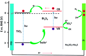
A facile and effective procedure for the synthesis of quasi-vertically aligned TiO2/Bi2S3 core–shell nanowire arrays (NWAs) is reported. The nontoxic and earth abundant Bi2S3 was assembled onto the hydrothermal pre-grown TiO2 NWAs via a successive ionic layer adsorption and reaction (SILAR) method. The morphologies, microstructures, and optical properties of the pristine TiO2 and composite TiO2/Bi2S3 with different SILAR circles were characterized in detail. For photoelectrochemical (PEC) measurements, the TiO2/Bi2S3 core–shell NWAs exhibited not only an enhanced photocurrent density (2.8 times higher than that of pristine TiO2), but also a negatively shifted onset potential from 0.067 to −0.072 V vs. RHE, as compared to the TiO2. This better PEC performance results from the broadened light absorption and the improved charge carrier separation efficiency. Our results provide a green photoelectrode for PEC hydrogen generation.
Introduction
Since the seminal work of Fujishima and Honda,1 titanium dioxide (TiO2) has been widely investigated as a photoanode material for photoelectrochemical (PEC) hydrogen production owing to its excellent chemical stability, low cost, nontoxicity and environment-friendly features.2–7 Among various nanostructured TiO2, the one dimensional TiO2 nanowire arrays (NWAs) on transparent FTO substrates have attracted considerable interest due to their facile fabrication, good oriented charge-transport properties, and large specific surfaces for light trapping.8–14 Despite these advantages, the photoconversion efficiencies of TiO2 NWA photoanodes are extremely depressed due to the large energy band gap (3.0 eV for rutile TiO2).15,16 This large energy band gap restricts their solar energy utilization only in the ultraviolet region. Therefore, considerable efforts have been made to enhance their visible light harvesting ability.17–23 For example, Wang et al. reported that the transition-metal doped TiO2 NWAs exhibited dramatically improved visible light absorptions and photocatalytic properties in comparison to the pristine TiO2 samples.24 Moreover, using morphology controlling strategies to design novel architectures is also explored to enhance the light utilization ability of TiO2, such as the branched TiO2 nanorod array electrode reported by Cho et al.25
Sensitizing TiO2 NWAs with short band gap semiconductors is another approach to extend the working spectrum into the visible range. In this case, the type-II heterostructure NWAs is integrated, and the light absorption can be extended by the narrower band gap sensitizers. In addition, the charge separation efficiency can also be largely improved due to the build-in space electric field. The conventional II–VI semiconductors such as CdS and CdSe, have exhibited considerable PEC performance improvement as sensitizers for TiO2 NWAs. However, their fatal toxicity is a worrying issue when used for practical applications. Recently, Bi2S3 has been emerging to be an effective, inexpensive and environmentally friendly light absorber material for wide band gap semiconductors.26 For example, Gao et al. reported the Bi2S3-coated BiVO4 discoids by in situ transform the surface BiVO4 into Bi2S3.27 The heterostructured BiVO4/Bi2S3 exhibited superior photocurrent response and photocatalytic activity for the reduction of CrVI under visible light illumination. Besides, Lin et al. demonstrated that the Bi2S3 quantum dots sensitized SnO2 porous film photoelectrode achieved a high photocurrent density of 0.9 mA cm−2 under 0.109 sun illumination.28 Also, there has been several reports on the hybridization of TiO2 with Bi2S3 for PEC application.29–31 For example, Zumeta-Dubé et al. reported the Bi2S3 quantum dots (QDs) sensitized TiO2-P25 with PEC conversion efficiency of 0.84%.32
In this paper, we report the heterostructured TiO2/Bi2S3 core–shell NWAs synthesized by successive ionic layer adsorption and reaction of Bi2S3 onto the pre-grown TiO2 NWAs for solar-light-driven PEC hydrogen generation. This hybrid TiO2/Bi2S3 outstands itself from the early reported TiO2/Bi2S3 composites by its one dimensional morphology. Comparing to the conventional II–VI semiconductors (such as CdS and CdSe) sensitized TiO2, this composite TiO2/Bi2S3 is environment-friendly and low-cost. The as-obtained photoanode exhibits strong absorption in the visible spectrum up to 800 nm. With light illumination, the optimized photoanode yields a photocurrent of ∼0.97 mA cm−2 at 0.2671 V vs. RHE, which is 2.8 times of that of pure TiO2 samples. Moreover, the TiO2/Bi2S3 composite photoanodes induce a cathodic shift of the photocurrent onset potential. The excellent PEC properties of our photoanodes show that the hybridization of Bi2S3 on the TiO2 NWAs has potential applications in QDs sensitized solar cells, PEC hydrogen generation and photocatalysis.
Experimental details
Preparation of TiO2 NWAs by hydrothermal method
TiO2 NWAs were grown onto fluorine-doped tin oxide (FTO) substrates using a hydrothermal method reported previously.33 Briefly, 0.45 ml titanium n-butoxide and 0.6 g NaCl were added into the 30 ml diluted hydrochloric acid (mass fraction 18.25–19%) and stirred until the mixture became clear. After that, the above precursor was transferred into a 100 ml Teflon-lined stainless steel autoclave in which the FTO substrates were placed with an angle against the in-wall with the conductive side facing down. The hydrothermal process was conducted in an electric oven at 150 °C for 8 h. After cooling, the resultant samples were removed and rinsed with water to get rid of any residual reactants and dried in air at 80 °C.
Preparation of Bi2S3-sensitized TiO2 NWAs by SILAR
For Bi2S3 sensitization, the as-synthesized TiO2 NWAs were successively immersed into two different solutions for 1 min each, first in 0.05 M Bi(NO3)3 solution and then in 0.1 M Na2S in aqueous solution. The Bi(NO3)3 solution was ultrasonic dissolved with the pH adjusted to 1–2 by concentrated nitric acid. Following each immersion, the electrodes were rinsed with deionized water and dried with a nitrogen stream to remove excess precursors before the next dipping. The two-step dipping procedure was called one SILAR cycle. Sample that went through n SILAR cycles is referred to as TiO2/Bi2S3(n). Finally, the as-prepared TiO2/Bi2S3 hybrid electrodes and the bare TiO2 electrode were annealed at 250 °C in Ar atmosphere for 1 hour.
Structural and optical characterizations
The morphology and microstructure of the samples were characterized using the field emission scanning electron microscope (NOVA NANOSEM 450, FEI, USA) equipped with an energy-dispersive X-ray spectroscopy (EDS) and transmission electron microscopy (TEM, JEM2010-HR, 200 kV). Raman spectra of the as-obtained samples were recorded on a Renishaw InVia system with a laser operating at λ = 532 nm as the excitation source. The crystal structure was characterized by a Rigaku Dmax 2500 X-ray diffractometer with Cu Kα radiation. The light absorption was recorded by UV-vis spectrophotometer (UV-2500, Shimadzu, Japan).
PEC measurements
The PEC properties of the photoelectrodes were studied on an electrochemical workstation (CH Instruments, model CHI660E). The three-electrode system was used with the TiO2 or TiO2/Bi2S3 NWAs on FTO substrates as the working electrodes, a Pt foil as counter electrode and Ag/AgCl as reference electrode. A mixture aqueous solution of 0.24 M Na2S and 0.35 M Na2SO3 (pH = 11.5) was used as the electrolyte and sacrificial reagent for all PEC measurements. A 150 W Xe lamp was used as the light source. Before test, the incident light intensity was calibrated to 100 mW cm−2 with a digital power meter. The photocurrent densities vs. measured potential (i–v curves) measurements were carried out at a scan rate of 25 mV s−1. The i–t curves were measured with a chopped light illumination at −0.6 V bias vs. Ag/AgCl. Electrochemical impedance spectroscopy (EIS) was measured under light at the open-circuit potential, with frequency range from 0.01 Hz to 100 kHz and the modulation amplitude of 5 mV. Mott–Schottky plots were measured in the dark at an AC frequency of 1.0 kHz. For all PEC measurements, the active area of the working electrodes was strictly kept within 1 cm2. Hereafter, the electrode potential versus the Ag/AgCl is converted to the reversible hydrogen electrode (RHE) potential according to the Nernst equation34
ERHE = EAg/AgCl + 0.059pH + EθAg/AgCl |
where ERHE is the converted potential vs. RHE, EθAg/AgCl = 0.1976 V at 25 °C, and EAg/AgCl is the experimental potential measured against the Ag/AgCl reference electrode.
Results and discussion
Fig. 1a shows the typical top view SEM image of the bare TiO2 NWAs. As seen, the TiO2 NWAs are uniformly grown on the entire substrate with diameter around 75 nm, and the rod exhibits a regular tetragonal growth. For composite photoanodes, we synthesized three TiO2/Bi2S3 core–shell NWAs samples with 10, 20 and 30 SILAR circles, and referred to them as TiO2/Bi2S3(10), TiO2/Bi2S3(20) and TiO2/Bi2S3(30), respectively. After the deposition of Bi2S3 layer, the surfaces of the TiO2 NW become rough. Fig. 1b shows the low magnification SEM image of the TiO2/Bi2S3 NWAs with 20 SILAR deposition circles. Compare to Fig. 1a, Bi2S3 modified TiO2 shows similar NWA feature but the image is slightly bright, suggest that the Bi2S3 sensitizers make the surfaces more conductive. Fig. 1c shows the morphology of the TiO2/Bi2S3(20) sample under higher magnification. As can be seen from Fig. 1c, Bi2S3 is uniformly deposited onto the TiO2 NW surfaces and the diameter TiO2/Bi2S3(20) is increased to approximately 100 nm. Hence, the Bi2S3 deposition thickness is approximately 13 nm. These observations indicate the successful synthesis of core–shell TiO2/Bi2S3 NWA heterostructures. The morphologies of the composite TiO2/Bi2S3 NWAs with different SILAR circles are also exhibited in Fig. S1(a)–(c) (see ESI†). With increasing of SILAR circles, a larger diameter and rougher surface of TiO2/Bi2S3 composite NWAs are displayed. In addition, some overdosed Bi2S3 nanoparticles are blocked at the interspaces of NWAs when the SILAR circles increased up to 30. This overloading of Bi2S3 is detrimental for PEC performance of TiO2/Bi2S3 photoelectrode which will be discussed later. The TEM images of the Fig. S1(d)–(f)† give a more straight-forward observation of the thickness of the Bi2S3 layer with different SILAR circles, from which we can also reckon the particle-initiated growth behavior of the Bi2S3 layer. When the SILAR circle is 10, only a few separated Bi2S3 particles are decorated on the TiO2 NW, the average diameter of the Bi2S3 particles is 20 nm. Increasing the SILAR circle up to 20, more Bi2S3 particles are loaded on the TiO2 NW (dark dot in Fig. S1e†), and the particles tend to interlink to each other resulting in an overall covering of the TiO2 NW surface. The 30 SILAR circles make a ∼25 nm thickness shell on the TiO2 NW (inset in Fig. S1f†), and the particle-stacked Bi2S3 shell can be directly seen. Fig. 1d displays the EDS spectrum of the TiO2/Bi2S3 NWAs, the atomic ratio of Bi
:
S is found to be ∼2
:
3, showing that the samples are in even stoichiometric. The other peaks of Ti, Si, Sn, Ca, and O are attributed to the chemical components of TiO2 NWAs and the FTO glass substrate. Fig. 1e shows the TEM image of TiO2/Bi2S3(20) core–shell NWs, it can be observed that the 1D TiO2 NW is sheathed by the Bi2S3 nanoparticles throughout the length. Fig. 1f is the HRTEM image taken from the red square in Fig. 1e. The observed interplanar spacing of 0.397 nm corresponds to the (220) plane of orthorhombic Bi2S3, which is agree with the result observed by XRD below.
 |
| Fig. 1 SEM images of bare TiO2 (a) and TiO2/Bi2S3(20) (b) NWAs, respectively. (c) Magnified SEM image of TiO2/Bi2S3(20) NWAs. (d) EDS of TiO2/Bi2S3(20) NWAs. TEM (e) and HRTEM (f) images of TiO2/Bi2S3(20) NWAs, respectively. | |
The XRD patterns of the as-obtained samples were collected to character their crystallographic phases (Fig. 2a). The pattern of the pristine TiO2 NWAs (black line in Fig. 2a) reveal that the TiO2 have a rutile structure (JPCDS 21-1276). Apart from the peaks of TiO2 and FTO substrate (JPCDS 77-0448), the additional diffraction peaks (red line in Fig. 2a) can be readily indexed to the orthorhombic phase of Bi2S3 (JCPDS 17-0320) for TiO2/Bi2S3 composite electrode. The main peaks at 2θ of 23.7, 24.9, 25.2, 28.6, and 31.76 are corresponding to the (101), (130), (310), (211) and (221) planes of orthorhombic Bi2S3, respectively. Fig. 2b shows the Raman spectra of the TiO2 and TiO2/Bi2S3 NWAs photoanodes. The pristine TiO2 exhibits two sharp peaks at 447 and 608 cm−1, which can be attributed to the Eg and A1g mode in rutile TiO2 as reported by Portq et al.35 The broad peak at 239 cm−1 is of a complex nature, which is relevant to the second-order scattering and disorder effects. The coating of Bi2S3 layer weakens characteristic peaks of the TiO2 and three new peaks at 237, 261 and 187 cm−1 are emerged. The added peaks can be attributed to the Ag, Bg1 and Ag mode of the Bi2S3,36,37 which indicates the crystalline character of Bi2S3 layer in the TiO2/Bi2S3 composite NWAs.
 |
| Fig. 2 (a) XRD patterns and (b) Raman scattering spectra of the pristine TiO2 and composite TiO2/Bi2S3 NWAs on FTO substrates. | |
The optical absorption properties of the TiO2 and TiO2/Bi2S3 were characterized by absorption spectra, as shown in Fig. 3. We can see that the absorption wavelength of TiO2 NWAs is less than 410 nm. In the case of the composite TiO2/Bi2S3 NWAs, its absorption extends to cover the whole visible light range and even beyond 800 nm. In addition, UV-vis absorption spectra show that as the SILAR deposition circle increases the light absorption ability also increases. The relationship between the incident photon energy and the absorption coefficient is given by the following equation: (αhν)2 = A(hν − Eg), where α, h, ν and Eg are the optical absorption coefficient, Planck constant, the photon frequency and band gap of semiconductor, respectively. A is a constant. The band-gap values of TiO2 and TiO2/Bi2S3(20) are derived to be 3.02 and 1.6 eV, respectively. This enhancement of light trapping effect for TiO2/Bi2S3(20) is beneficial for the PEC hydrogen generation application.
 |
| Fig. 3 Normalized UV-vis absorption spectra of TiO2 and TiO2/Bi2S3 core–shell NWAs on FTO substrates. | |
To evaluate the Bi2S3 sensitization effect on PEC performance of TiO2, Fig. 4a shows the i–v curves of the bare TiO2 and the TiO2/Bi2S3 core–shell NWAs with 10, 20 and 30 SILAR circles. By analyzing the experimental data in Fig. 4a, three conclusions can be reached. First, for all of the TiO2/Bi2S3 NWAs photoanodes, the saturate photocurrent densities are much higher than that of the pristine TiO2. The TiO2/Bi2S3(20) sample achieved a value of 0.98 mA cm−2 at 0.2671 V vs. RHE (−0.6 V vs. Ag/AgCl), which is higher than that of the bare TiO2 (0.35 mA cm−2) and other composite photoanodes (0.8 mA cm−2 for TiO2/Bi2S3(10) and 0.95 mA cm−2 for TiO2/Bi2S3(30)). It confirms that the coating of Bi2S3 is a simple but effective method for enhancing the PEC performance of TiO2. Second, as compared to TiO2, the onset potential of TiO2/Bi2S3 is much negatively shifted and leads to the photocurrent saturation at a more negative potential. Typically, the photocurrent increases from the onset potential around −0.072 V vs. RHE and approaches a plateau at 0.05 V vs. RHE for TiO2/Bi2S3(20) sample, whereas the photocurrent plateau in the bare TiO2 photoanode is 0.3 V vs. RHE. Achieving the saturated photocurrent level at a more negative potential is significantly important because it reduces the applied external bias, and thus increases the overall efficiency of the PEC cells.22 Third, the TiO2/Bi2S3(20) overmatches the one with 10 or 30 SILAR circles deposition. As the Bi2S3 deposition increasing, the light absorption of TiO2/Bi2S3 is also increased (see Fig. 3). However, too much Bi2S3 deposition blocks the porous structure of the electrodes (see SEM images of Fig. S1 in ESI†) and lengthens the electron diffusion path from Bi2S3 to TiO2. In this case, a more positive external bias is needed to separate the photo-induced charge efficiently for TiO2/Bi2S3(30), which can explain the smaller photocurrent between 0 and 0.3 V vs. RHE but similar photocurrent when the potential exceeds 0.35 V vs. RHE in comparison with TiO2/Bi2S3(20). Fig. 4b shows the i–t curves of the TiO2 and the TiO2/Bi2S3 core–shell NWAs photoelectrodes at 0.2671 bias vs. RHE under chopped light irradiation. Upon illumination, the photocurrent of TiO2/Bi2S3 flashily rise to a high level, and decay to a relatively steady-state after a few second, displaying a series of spikes in the photoresponse. This behavior might be attributed to the charge carrier accumulation at the electrode–electrolyte interface due to the slow oxygen evolution kinetics or oxidization of trap states on the surface and in the bulk by charge carriers.38 And when the light is cut off, the photocurrent densities drop to nearly zero instantaneously. Such fast rise and fall of the photocurrents indicates that carrier transport in the heterojunction material proceeds very quickly.
 |
| Fig. 4 (a) i–v curves under AM 1.5G in the dark and at 100 mW cm−2 illumination for pristine TiO2 NWAs and TiO2/Bi2S3 core–shell NWAs with different circles SILAR. (b) Amperometric i–t curves of the TiO2/Bi2S3(10, 20, 30) core–shell NWAs at 0.2761 V versus RHE with light on/off cycles. | |
Fig. 5a shows the Mott–Schottky (M–S) plots, in which the flat band potential at the electrode–electrolyte interface can be estimated by the M–S equation39
1/C2 = (2/εε0eNdA2)[(V − VFB) − kT/e0] |
where
C is the specific capacity,
ε is the dielectric constant of Bi
2S
3 or TiO
2,
ε0 is the electric permittivity of vacuum,
Nd is the carrier density,
A is the area,
V is the applied potential,
VFB is the flat band potential,
k is the Boltzmann constant,
T is the absolute temperature, and
e0 is the electron charge. The
VFB values of the TiO
2/Bi
2S
3 and TiO
2 NWAs are determined to be 0.07 V and 0.26 V
vs. RHE by extrapolating the
X-intercepts of the linear region in the M–S plot, respectively. Such a negative shift of the flat band for the TiO
2/Bi
2S
3 electrode suggests a higher carrier concentration and lower charge recombination in the TiO
2/Bi
2S
3 electrode in comparison with the pristine TiO
2. In addition, the positive slope indicates that the TiO
2/Bi
2S
3 NWA is an n-type semiconductor. The TiO
2/Bi
2S
3 shows substantially smaller M–S plot slope compared to the TiO
2, suggesting an increase of donor density in the TiO
2/Bi
2S
3.
9 Using the resulted
VFB and band gap values of the TiO
2/Bi
2S
3 and TiO
2, the energy band level aliments can be estimated as displayed in
Fig. 5b.
40 The charge transfer and hydrogen production mechanism in the TiO
2/Bi
2S
3 PEC cell is proposed. When the TiO
2/Bi
2S
3 heterojunction is irradiated by solar light, electrons are excited to the conduction band (CB) of Bi
2S
3 and TiO
2. Subsequently, electrons migrate from Bi
2S
3 to TiO
2 and finally to the counter electrode to produce H
2. At the same time, the holes are transported to the valence band (VB) of Bi
2S
3 and then scavenged by the sacrificial reagents at the electrode–electrolyte interface. Thus, the photogenerated charge separation efficiency is improved because of the formation of type-II heterojunction interface in the TiO
2/Bi
2S
3 electrode, which is also responsible for its high photocurrent density.
 |
| Fig. 5 (a) Mott–Schottky plots of pristine TiO2 and TiO2/Bi2S3(20) core–shell NWAs. (b) Schematic of energy band level aliment and carrier transferring mechanism in TiO2/Bi2S3 core–shell NWAs. (c) Nyquist plots and (d) Bode plots of the impedance spectra measured at open circuit condition under 1 sun illumination. | |
To further examine the intrinsic electronic properties of the TiO2/Bi2S3 NWAs, the EIS were collected and shown in Fig. 5c. Normally, the smaller the radius in Nyquist plot, the lower the charge transfer impedance at the electrode–electrolyte interface for corresponding electrode.41 The TiO2/Bi2S3 composite electrodes represent much smaller radius than the pristine TiO2 electrode, implying its more effective charge carrier separations compared to the pristine TiO2. The inset in the Nyquist plots is the equivalent circuit model of the PEC cell, where the Rs is the series resistance of the electrochemical device, R and C represent the resistance and capacitance of space charge region, respectively, including charge transfer across the FTO/TiO2–Bi2S3 interface and the TiO2–Bi2S3/electrolyte interface, RPt and CPt are the resistance and capacitance of the Pt cathode, respectively. By fitting the experimental data (dot points) into solid line using the equivalent circuit model, a more quantitative approach to compare the interface charge transfer impedance of TiO2 and TiO2/Bi2S3 is reached. As a result, the determined value of R is 3270 and 735 Ω for pristine TiO2 and composite TiO2/Bi2S3 photoelectrodes, respectively. Correspondingly, the TiO2/Bi2S3 heterojunction shows a lower characteristic peak frequency in the Bode phase plot in Fig. 5d, implying the longer electron lifetime than that of the pristine TiO2 electrode.42 The enhanced charge separation and prolonged electron lifetime in the TiO2/Bi2S3 composite is also responsible for the improved PEC performance for TiO2.
Conclusions
In summary, we have successfully synthesized the TiO2/Bi2S3 core–shell NWAs as photoelectrode for PEC hydrogen generation. The coating of Bi2S3 layer achieves a remarkable enhancement of photocurrent density in the TiO2 NWAs photoanode. Moreover, the onset potential of the composite photoanode is also largely shifted to a negative direction. The broadened light absorption and improved charge carrier separation efficiency in the type-II TiO2/Bi2S3 core–shell NWAs are responsible for the PEC performance enhancement. The present work provides a new photoelectrode with non-toxicity, low cost and easy fabrication, which may have potential application in PEC hydrogen generation and photocatalysis.
Acknowledgements
We thank the financial support of the National Natural Science Foundation of China (Grant no. 51202208, 51172191, and 11274264), The Project supported by Scientific Research Fund of Hunan Provincial Education Department (Grant no. 12B129), National Basic Research Program of China (no. 2012CB921303) and the Program for Changjiang Scholars and Innovative Research Team in University (IRT13093).
References
- A. Fujishima and K. Honda, Nature, 1972, 238, 37–38 CrossRef CAS.
- S. U. M. Khan, Science, 2002, 297, 2243–2245 CrossRef CAS PubMed.
- I. Mora-Seró, T. L. Villarreal, J. Bisquert, Á. Pitarch, R. Gómez and P. Salvador, J. Phys. Chem. B, 2005, 109, 3371–3380 CrossRef PubMed.
- P. R. Mishra, P. K. Shukla and O. N. Srivastava, Int. J. Hydrogen Energy, 2007, 32, 1680–1685 CrossRef CAS PubMed.
- J. H. Pan, X. Z. Wang, Q. Huang, C. Shen, Z. Y. Koh, Q. Wang, A. Engel and D. W. Bahnemann, Adv. Funct. Mater., 2014, 24, 95–104 CrossRef CAS.
- H. Cui, W. Zhao, C. Yang, H. Yin, T. Lin, Y. Shan, Y. Xie, H. Gu and F. Huang, J. Mater. Chem. A, 2014, 2, 8612 CAS.
- X. Zhang and Z. Chen, RSC Adv., 2015, 5, 9482–9488 RSC.
- Q. Dong, H. Yu, Z. Jiao, G. Lu and Y. Bi, RSC Adv., 2014, 4, 59114–59117 RSC.
- Q. Kang, J. Cao, Y. Zhang, L. Liu, H. Xu and J. Ye, J. Mater. Chem. A, 2013, 1, 5766 CAS.
- W. Wu, B. Lei, H. Rao, Y. Xu, Y. Wang, C. Su and D. Kuang, Sci. Rep., 2013, 3, 1352, DOI:10.1038/srep01352.
- P. Roy, D. Kim, K. Lee, E. Spiecker and P. Schmuki, Nanoscale, 2010, 2, 45 RSC.
- B. Liu and E. S. Aydil, J. Am. Chem. Soc., 2009, 131, 3985–3990 CrossRef CAS PubMed.
- A. Wolcott, W. A. Smith, T. R. Kuykendall, Y. Zhao and J. Z. Zhang, Small, 2009, 5, 104–111 CrossRef CAS PubMed.
- K. Hara, K. Sayama, H. Arakawa, Y. Ohga, A. Shinpo and S. Suga, Chem. Commun., 2001, 569–570 RSC.
- N. Jain, Y. Zhu, D. Maurya, R. Varghese, S. Priya and M. K. Hudait, J. Appl. Phys., 2014, 115, 24303 CrossRef PubMed.
- D. O. Scanlon, C. W. Dunnill, J. Buckeridge, S. A. Shevlin, A. J. Logsdail, S. M. Woodley, C. R. A. Catlow, M. J. Powell, R. G. Palgrave, I. P. Parkin, G. W. Watson, T. W. Keal, P. Sherwood, A. Walsh and A. A. Sokol, Nat. Mater., 2013, 12, 798–801 CrossRef CAS PubMed.
- Q. Liu, H. Lu, Z. Shi, F. Wu, J. Guo, K. Deng and L. Li, ACS Appl. Mater. Interfaces, 2014, 6, 17200–17207 CAS.
- M. Khan, P. Jiang, J. Li and W. Cao, J. Appl. Phys., 2014, 115, 153103 CrossRef PubMed.
- C. Dette, M. A. Pérez-Osorio, C. S. Kley, P. Punke, C. E. Patrick, P. Jacobson, F. Giustino, S. J. Jung and K. Kern, Nano Lett., 2014, 14, 6533–6538 CrossRef CAS PubMed.
- Y. Li, W. Wu, P. Dai, L. Zhang, Z. Sun, G. Li, M. Wu, X. Chen and C. Chen, RSC Adv., 2014, 4, 23831 RSC.
- S. Kurian, H. Seo and H. Jeon, J. Phys. Chem. C, 2013, 117, 16811–16819 CAS.
- G. Wang, H. Wang, Y. Ling, Y. Tang, X. Yang, R. C. Fitzmorris, C. Wang, J. Z. Zhang and Y. Li, Nano Lett., 2011, 11, 3026–3033 CrossRef CAS PubMed.
- B. Liu, H. M. Chen, C. Liu, S. C. Andrews, C. Hahn and P. Yang, J. Am. Chem. Soc., 2013, 135, 9995–9998 CrossRef CAS PubMed.
- C. Wang, Z. Chen, H. Jin, C. Cao, J. Li and Z. Mi, J. Mater. Chem. A, 2014, 2, 17820–17827 CAS.
- I. S. Cho, Z. Chen, A. J. Forman, D. R. Kim, P. M. Rao, T. F. Jaramillo and X. Zheng, Nano Lett., 2011, 11, 4978–4984 CrossRef CAS PubMed.
- T. Wu, X. Zhou, H. Zhang and X. Zhong, Nano Res., 2010, 3, 379–386 CrossRef CAS PubMed.
- X. Gao, H. B. Wu, L. Zheng, Y. Zhong, Y. Hu and X. W. D. Lou, Angew. Chem., Int. Ed., 2014, 53, 5917–5921 CrossRef CAS PubMed.
- Y. C. Lin and M. W. Lee, J. Electrochem. Soc., 2013, 161, H1–H5 CrossRef PubMed.
- J. Kim and M. Kang, Int. J. Hydrogen Energy, 2012, 37, 8249–8256 CrossRef CAS PubMed.
- R. Brahimi, Y. Bessekhouad, A. Bouguelia and M. Trari, Catal. Today, 2007, 122, 62–65 CrossRef CAS PubMed.
- L. M. Peter, K. G. U. Wijayantha, D. J. Riley and J. P. Waggett, J. Phys. Chem. B, 2003, 107, 8378–8381 CrossRef CAS.
- I. Zumeta-Dubé, V. Ruiz-Ruiz, D. Díaz, S. Rodil-Posadas and A. Zeinert, J. Phys. Chem. C, 2014, 118, 11495–11504 Search PubMed.
- G. Ai, R. Mo, H. Xu, Q. Chen, S. Yang, H. Li and J. Zhong, J. Appl. Phys., 2014, 116, 174306 CrossRef PubMed.
- M. Gratzel, Nature, 2001, 414, 338–344 CrossRef CAS PubMed.
- S. P. S. Portq, P. A. Fleury and T. C. Damen, Phys. Rev., 1967, 154, 522 CrossRef.
- T. Lutz, A. MacLachlan, A. Sudlow, J. Nelson, M. S. Hill, K. C. Molloy and S. A. Haque, Phys. Chem. Chem. Phys., 2012, 14, 16192 RSC.
- Y. Zhao, K. T. E. Chua, C. K. Gan, J. Zhang, B. Peng, Z. Peng and X. Qihua, Phys. Rev. B: Condens. Matter Mater. Phys., 2011, 84, 205330 CrossRef.
- S. K. Pilli, T. E. Furtak, L. D. Brown, T. G. Deutsch, J. A. Turner and A. M. Herring, Energy Environ. Sci., 2011, 4, 5028 CAS.
- T. Majumder, J. J. L. Hmar, K. Debnath, N. Gogurla, J. N. Roy, S. K. Ray and S. P. Mondal, J. Appl. Phys., 2014, 116, 34311 CrossRef PubMed.
- A. B. Ellis, S. W. Kaiser, J. M. Bolts and M. S. Wrighton, J. Am. Chem. Soc., 1977, 99, 2839–2848 CrossRef CAS.
- Y. Hou, F. Zuo, A. Dagg and P. Feng, Angew. Chem., 2013, 125, 1286–1290 CrossRef.
- Q. Liu, H. Lu, Z. Shi, F. Wu, J. Guo, K. Deng and L. Li, ACS Appl. Mater. Interfaces, 2014, 6, 17200–17207 CAS.
Footnote |
† Electronic supplementary information (ESI) available. See DOI: 10.1039/c4ra15820b |
|
This journal is © The Royal Society of Chemistry 2015 |
Click here to see how this site uses Cookies. View our privacy policy here.