A nanopoint Schottky-gate array device: surface defect application and molecular detection

Chun-Han Sung, Tzu-Chiao Chien, Chih-Ming Chang, Chien-Min Chang and Ping-Hung Yeh*
Department of Physics, Tamkang University, Tamsui, New Taipei City, 25137, Taiwan. E-mail: phyeh331@mail.tku.edu.tw

Received 4th December 2014 , Accepted 7th January 2015

First published on 7th January 2015


Abstract

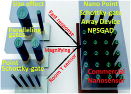
We have demonstrated a nanopoint Schottky-gate array device (NPSGAD) which can enhance the sensitivity, the signal current output level and the distinguishability by placing numerous ZnO point Schottky-gates in parallel gigantically. By using NPSGADs, we can improve the current output to the order of mA and enhance the CO sensor detection ability to room temperature detection. NPSGADs can achieve the above-mentioned properties based on several designs, e.g. point Schottky-gate can enhance detection response, parallel Schottky-gate can enhance the gas monitor levels and Schottky-gate array can reduce the total resistance for high signal current output. For UV light detection, NPSGADs can achieve a signal current of 8 mA. For room temperature detection of CO, the signal current can be enhanced above 0.25 mA. Note that these signal levels can already be used for commercial application. The gas detection signal also can be improved by increasing the operating temperature; moreover, the current variation averages of CO detection of the NPSGAD are 1.7 mA, 10.1 mA and 14.9 mA at operating temperatures of 150 °C, 350 °C and 400 °C, respectively.


Introduction

Recently, there have been numerous studies about the considerable improvement of the photo, gas, and chemically-charged molecules detection using core/shell structure, Schottky-gate nanosensors (SGNS) and nanostructures.1–8 In regard to SGNS, high resistivity is a major hindrance for increasing the current output level for commercial application. To improve the current output, multi-channel devices were used in several research fields such as photodetectors,9,10 gas sensors,11,12 biomolecular detectors,13,14 nanogenerators15,16 and solar cells.17,18 The greatest advantage of multi-channel devices is that they can improve the current output level for commercial application by putting numerous nanowires in parallel. In addition, some researchers have also indicated that different electronic contacts also affect electronic transportation.19 Due to these reasons, multi-channel devices will play an essential role in future research. In this work, we demonstrated a nanopoint Schottky-gate array device to improve the detection ability of nanosensors. Despite the fact that using multi-channel devices to replace single nanowire devices is the way to increase the current level, there have been some unknown issues that should be clarified.

Results and discussion

ZnO NWs can be prepared by the standard solid-vapor process20,21 and hydrothermal growth.22 To investigate Schottky-gate size effect, a series of Schottky-gate devices (SGDs) can be fabricated using crystalline ZnO NWs, which were placed on Pt electrode patterns, and then Pt[thin space (1/6-em)]:[thin space (1/6-em)]Ga was deposited on the ZnO NWs to form ohmic contacts using a focus ion beam (FIB) system.4–6 For Schottky contacts, ZnO NWs were placed on a Pt electrode pattern, the natural contacts of which are mainly Schottky type. The current–voltage (IV) characteristic of the SGDs of different size (5 and 10 μm) are shown in Fig. 1(a); in this research work, we developed a nanopoint Schottky-gate (NPSG) device, whose IV characteristic output can be seen in Fig. 1(b). All these SGDs show great rectification ability. For gas detection, oxygen (O2) and carbon monoxide (CO) are the gases that deserve to be mentioned. For example, O2 is an oxidant for classical codices and famous paintings and CO is a toxic gas for human beings; thus, both need high sensitivity and fast response detection. Compared with the CO detection ability of these three SGDs, the response time of the NPSG (0.2 μm Schottky-gate areas) is faster than the other two SGDs (5 and 10 μm Schottky-gate areas, as shown in Fig. 1(c)). The response time of various Schottky-gate areas (10 μm, 5 μm and 0.2 μm) is around 800, 264 and 141 s. Oxygen absorption on the Schottky-gate can increase the Schottky barrier height (SBH) causing a low current, but carbon monoxide absorption on the Schottky-gate can decrease the SBH and produce a high current.4 The SBH variation (Δϕ) is equal to the summation of effective SBH and the O2/CO absorption changed barrier height (Δϕ = ϕS + ϕO2ϕCO), as shown in the inset of Fig. 1(d).
image file: c4ra15763j-f1.tif
Fig. 1 (a) and (b) represent the IV curves and schematic diagram of 5/10 μm and nanopoint Schottky-gate devices, respectively. (c) The CO sensing ability of Schottky-gate devices of different sizes under 250 °C. (d) Schematic of O2 and CO2 absorption relative to surface oxygen vacancy concentration. Small Schottky-gate sizes can be easily switched by gas molecules.

Reducing the Schottky-gate area can compel the NPSG to have a faster response; it just needs fewer gas molecules to switch the Schottky-gate. The density of surface oxygen vacancies should be consistent with those of the ZnO NWs (the ZnO NWs were synthesized in the same batch); thus, reducing the Schottky-gate area would have fewer oxygen vacancies on the surface and would only need less gas absorption to tune the SBH for switching the Schottky-gate, as illustrated in Fig. 1(d). However, the different CO levels cannot be monitored. On the contrary, the increasing Schottky-gate area would enhance gas absorption, and then differentiate the signal of various CO levels (Fig. S1). For different Schottky-gate size SGDs, we can also see that the current keeps increasing, as represented by the blue line in Fig. 1(c): the larger Schottky-gate area can detect more gas levels, but the response time will be longer to achieve saturation. The schematic is related to surface oxygen vacancy concentration for O2 and CO absorption as illustrated in Fig. 1(d). To solve above contradiction, we provide a design to enable faster monitoring speed and differentiate various gas levels.

To differentiate various gas levels, we need to find a solution to increase the Schottky-gate area, but still need to maintain a faster monitoring speed. For this purpose, we placed two SGDs (5 μm Schottky-gate areas) in parallel to double the Schottky-gate area. Both SEM image and schematic of ZnO NWs dual-SGDs are illustrated in Fig. 2(a). In this experiment, the total resistance also can be reduced by paralleling the Schottky-gates, namely, dual channel dual Schottky-gate device (DCDS). For ZnO NWs SGD, resistances, which include Schottky contact resistance (Rs), ohmic contact resistance (Ro) and nanowire resistance (Rw), are always the main issue that dominate the signal value of the sensor. Among these three types of resistance, Rs has the highest resistance, which is the main issue that limits the signal current output.23 Typical IV curves of SGDs indicate that each SGD performs well as an excellent diode and rectification under reverse bias. In the IV curves, the pink and light blue lines in the IV curve represent the individual single channel single Schottky-gate device (SCSS), as shown in Fig. 2(b). The output current level of the DCDS could be enhanced by decreasing the total resistance; however, whether decreasing the total resistance will affect the detection characteristics (sensitivity and reset time) of the ZnO SGD or not, which needs to be clarified. The DCDS and SCSS were operated under reverse bias (−1 V) and UV light sensing ability was measured, as shown in Fig. 2(c). The signal current output levels of the SCSS and DCDS are 90 nA and 174 nA, respectively; moreover, the signal current output level of DCDS is almost double that of SCSS. Based on Kirchhoff's circuit law, the current values of the DCDS are approximately equal to the sum of the current of the two individual SCSSs. The sensitivity of the SCSS and DCDS are 1394% and 1828%, respectively. From the electric measurement, the ideality factor and Schottky barrier height (SBH) can be calculated.23 Note that the ideality factors of the SCSS and DCDS are 1.46 and 1.62, respectively. There are several parameters that affect the ideality factor, such as interface state, thermionic-field emission (TFE), image force lowering, generation/recombination current and temperature. In our study, only interface state will be the parameter to vary the ideality factor for these SGDs. Note that the DCDS has much more interface state compared with the SCSS; thus, the ideality factor of the DCDS is higher than the SCSS. When ideality factor is between one and two, the electronic transportation behavior is dominated by TFE.24 Using thermionic-field emission as the electric transportation mechanism, the SBH would be the import parameter for SGD sensing. The SBHs formed by connecting ZnO NWs and Pt electrode of these nanodevices were found to be around 0.54 eV, which is close to the ideal SBH.25,26 By placing SGDs in parallel (such as DCDS), we can not only lower the total resistance to increase the signal current output level, but also increase the Schottky-gate area to enhance sensitivity. The stability of UV light measurement of the SCSS and DCDS is shown Fig. 2(d). Thus, reducing the total resistance by placing Schottky-gates in parallel will not degrade the detection characteristics (sensitivity and reset time) of ZnO SGD.


image file: c4ra15763j-f2.tif
Fig. 2 (a) and (b) show the schematic diagram/SEM image and the IV curves/basic circuits of Schottky-gate devices, respectively. Pink and light blue lines represent the individual current of each single channel single Schottky-gate device (SCSS), while the red line represents the current of the dual channel dual Schottky-gate device (DCDS). The scale bar of the inset is 5 μm. (c) The UV light detection signal of the DCDS (174 nA) is almost twice as high as the SCSS (90 nA). Inset: the schematic diagram/basic circuit of the SCSS and DCDS. (d) The stability of UV light measurement of the SCSS and DCDS is shown.

Furthermore, we should clarify if the various gas levels can be differentiated by increasing the Schottky-gate numbers (or area). First, the signal current outputs of these SGDs were measured in a vacuum; thus, the current in the vacuum can be seen as the base current before O2 and CO sensing. This step gives us a clean detection environment for O2 and CO sensing; and simplifies the detection condition without the effect of other gases. For CO sensing, the DCDS has improved both sensitivity and signal current output, compared with the SCSS. For both DCDS and SCSS, the signal current outputs increased with raising CO concentration, as shown in Fig. 3(a). The DCDS has faster response and enhances the sensitivity from 3000% to 6500% for 320 ppm CO concentration under 250 °C, compared with the SCSS. Based on the monitor data, the various CO levels can be differentiated using the DCDS. However, for the SCSS, the CO level cannot be differentiated when the CO concentration is above 80 ppm, as shown in Fig. 3(b). The reason why the DCDS can distinguish the gas concentration difference is that the DCDS has a larger detection area than the SCSS. Proposed mechanisms for the gas absorption of the SCSS and DCDS are indicated in Fig. 3(c) and (d). CO sensing mechanism of the DCDS is illustrated in Fig. 3(c), DCDS has twice Schottky-gate area to detect CO molecules. Once the device is operated in an O2 environment, many O2 molecules will be absorbed on the ZnO nanowire and become O2; this is the reason why the SBH is higher in oxygen than that in a vacuum environment.1,2 On the other hand, CO absorbs O2 on the surface of the ZnO nanowire and becomes carbon dioxide; thus, the SBH gets reduced. Thus, we observe that the sensitivity increases with the increasing concentration of CO, consistent with Scott's theory.27,28 Placing two SGDs in parallel to form the DCDS can not only improve the different gas levels monitoring ability but also enhance the signal current output level. The DCDS appears to have dual Schottky-gates to detect the gas and to control the current flow, as illustrated in Fig. 3(d). In a previous work and this work, the SCSS cannot differentiate gas concentrations over 100 ppm;4 but the different gas concentration detection ability of the DCDS is far greater than the SCSS.


image file: c4ra15763j-f3.tif
Fig. 3 (a) and (b) show that DCDS has rapid response and higher sensitivity than the SCSS for CO sensing. Proposed mechanisms of the SBH variation controlled SCD are indicated in (c) and (d). The DCDS seems to have dual Schottky-gates to detect the gas and to control the current flow. Here, only one Schottky-gate is activated and the other Schottky-gate is steady in (d), which illustrates the control ability of DCDS.

Based on the above-mentioned data, we need NPSGs to have fast response and multiple Schottky-gates for sensitivity and signal current level enhancement. Here, we demonstrated that the nanopoint Schottky-gate array device (NPSGAD) can achieve room temperature gas detection and enhance the signal output level to the order of mA (not laboratory level measurement, nA or μA). Note that these two enhancements can improve the commercial application of ZnO NW devices. A NPSGAD was designed with two ideas: (i) nanopoint Schottky-gate (NPSG) that can enhance the response time because the Schottky-gate can be easily switched if the contact surface is narrowed down to a nanopoint, and (ii) the signal output level would be amplified because NPSGAD places thousands of NPSG in parallel, which will increase the detection area and lower the total resistance to improve the gas monitor levels and signal current output, respectively, as illustrated in Fig. 4(a). The UV light signal current output of NPSGAD enhanced to the order of mA, which can considerably improve the commercial potential of NPSGAD, as shown in Fig. 4(b). Moreover, the room temperature CO detection is the most inspiring enhancement of NPSGAD for commercial application, as shown in Fig. 4(c). Note that the current signal keeps increasing because the CO molecules keep getting absorbed on the Schottky-gates; thus, the Schottky-gate barriers keep lowering, and then more electrons can pass the Schottky-gates to form a signal current. For our experiment, the NPSG device is extremely sensitive to its environment. The point contact area can create high current density for Joule heating effect, which mainly increases the temperature at the point contact interface, i.e., the Schottky-gate area, which is the absorption area for gas molecules. For a gas sensor, previously reported studies mentioned that need a high operating temperature is required to increase the absorption of gas molecules. The NPSG device provides a self-heating effect and just heats the detection area, i.e., Schottky-gate, as shown in Fig. S2. Based on the above-mentioned idea, we can use the NPSG as a detection unit for the NPSGAD and place thousands of NPSGs in parallel, which can reduce the gas absorption temperature and improve the current output level. The signal variation averages of CO detection of NPSGAD are 1.7 mA, 10.1 mA and 14.9 mA at the operating temperatures of 150 °C, 350 °C and 400 °C, respectively. The gas molecules absorbed on the Schottky-gate might be physically absorbed at low temperatures (150 °C) and might be chemically absorbed at high temperatures (250 °C). For the NPSGAD, the nanopoint Schottky-gate is very sensitive and can be triggered easily with gas absorption, and this property enables its application as a gas sensor.


image file: c4ra15763j-f4.tif
Fig. 4 (a) NPSGAD places thousands of NPSG in parallel, which can increase the detection area and lower the total resistance. (b) The UV light signal current output of the NPSGAD enhanced to mA order. (c) The room temperature CO detection is the most important enhancement of the NPSGAD for commercial application. (d) The signal variation averages of CO detection of the NPSGAD are 1.7 mA, 10.1 mA and 14.9 mA at operating temperatures of 150 °C, 350 °C and 400 °C, respectively.

Conclusion

We have demonstrated a design for ZnO NW nanosensors that provides considerable enhancement in sensitivity and the signal current output by placing Schottky-gates in parallel. Using a NPSG can enhance the gas detection response, using a DCDS for UV light detection, the signal current level and the sensitivity can be improved from 90 to 174 nA and from 1394% to 1828%, compared with a SCSS, respectively. For O2 sensing, the DCDS has rapid response and enhances the sensitivity from 130[thin space (1/6-em)]000% to 740[thin space (1/6-em)]000%, which is about six-fold higher than that of SCSS. For CO sensing, the different gas concentration levels can be monitored using the DCDS. NPSGAD combined several ideas, such as point Schottky-gate, paralleling Schottky-gates and Joule heating effect, to achieve high speed monitoring of various gas levels and room temperature gas detection. Placing numerous nanopoint Schottky-gates in parallel, not only can lower the total resistance to increase the signal current level, but also can enlarge the Schottky-gates sensing area to enhance the gas monitoring levels. In particular, when the size and number of Schottky-gate are narrowed to nanopoint scale and increased to thousands, the gas monitoring ability can be considerably enhanced for room temperature detection and mA order current output. The illustrated methodology and principle present a unique sensing concept that can be readily and extensively applied to other sensor systems.

Acknowledgements

This research was supported by the National Science Council of the Republic of China (Taiwan) under grants NSC-98-2112-M-032-003-MY3 and NSC-101-2112-M-032-004-MY3.

References

  1. Z. Yang, L. Guo, B. Zu, Y. Guo, T. Xu and X. Dou, Adv. Opt. Mater., 2014, 2, 738–745 CrossRef CAS.
  2. T.-Y. Wei, P.-H. Yeh, S.-Y. Lu and Z. L. Wang, J. Am. Chem. Soc., 2009, 131, 17690–17695 CrossRef CAS PubMed.
  3. J. Zhou, Y. Gu, Y. Hu, W. Mai, P.-H. Yeh, G. Bao, A. K. Sood, D. L. Polla and Z. L. Wang, Appl. Phys. Lett., 2009, 94, 191103 CrossRef PubMed.
  4. P.-H. Yeh, Z. Li and Z. L. Wang, Adv. Mater., 2009, 21, 4975–4978 CrossRef CAS PubMed.
  5. R. Dong, C. Bi, Q. Dong, F. Guo, Y. Yuan, Y. Fang, Z. Xiao and J. Huang, Adv. Opt. Mater., 2014, 2, 549–554 CrossRef CAS.
  6. R.-E. Nowak, M. Vehse, O. Sergeev, T. Voss, M. Seyfried, K. von Maydell and C. Agert, Adv. Opt. Mater., 2014, 2, 94–99 CrossRef CAS.
  7. C.-Y. Lai, T.-C. Chien, T.-Y. Lin, T. Ke, S.-H. Hsu, Y.-J. Lee, C.-y. Su, J.-T. Sheu and P.-H. Yeh, Nanoscale Res. Lett., 2014, 9, 281 CrossRef PubMed.
  8. J. K. Hsu, T. Y. Lin, C. Y. Lai, T. C. Chien, J. H. Song and P. H. Yeh, Appl. Phys. Lett., 2013, 103, 123507 CrossRef PubMed.
  9. J. A. Czaban, D. A. Thompson and R. R. LaPierre, Nano Lett., 2008, 9, 148–154 CrossRef PubMed.
  10. Q. Zheng, B. Zhou, J. Bai, L. Li, Z. Jin, J. Zhang, J. Li, Y. Liu, W. Cai and X. Zhu, Adv. Mater., 2008, 20, 1044–1049 CrossRef CAS.
  11. J. Gong, Y. Li, X. Chai, Z. Hu and Y. Deng, J. Phys. Chem. C, 2009, 114, 1293–1298 Search PubMed.
  12. H.-W. Ra, K.-S. Choi, J.-H. Kim, Y.-B. Hahn and Y.-H. Im, Small, 2008, 4, 1105–1109 CrossRef CAS PubMed.
  13. H. R. Byon and H. C. Choi, J. Am. Chem. Soc., 2006, 128, 2188–2189 CrossRef CAS PubMed.
  14. S. N. Kim, J. F. Rusling and F. Papadimitrakopoulos, Adv. Mater., 2007, 19, 3214–3228 CrossRef CAS PubMed.
  15. Z. L. Wang and J. Song, Science, 2006, 312, 242–246 CrossRef CAS PubMed.
  16. A. Yu, P. Jiang and Z. Lin Wang, Nano Energy, 2012, 1, 418–423 CrossRef CAS PubMed.
  17. K.-Q. Peng and S.-T. Lee, Adv. Mater., 2011, 23, 198–215 CrossRef CAS PubMed.
  18. E. C. Garnett, M. L. Brongersma, Y. Cui and M. D. McGehee, Annu. Rev. Mater. Res., 2011, 41, 269–295 CrossRef CAS.
  19. F. Leonard and A. A. Talin, Nat. Nanotechnol., 2011, 6, 773–783 CrossRef CAS PubMed.
  20. Z. W. Pan, Z. R. Dai and Z. L. Wang, Science, 2001, 291, 1947–1949 CrossRef CAS PubMed.
  21. W. Zhong Lin, J. Phys.: Condens. Matter, 2004, 16, R829 CrossRef.
  22. D. Sunandan Baruah and J. Dutta, Sci. Technol. Adv. Mater., 2009, 10, 013001 CrossRef.
  23. J. B. Baxter and C. A. Schmuttenmaer, J. Phys. Chem. B, 2006, 110, 25229–25239 CrossRef CAS PubMed.
  24. S. Sze, Physics of Semiconductor Device, Wiley, 1987, ch. 5 Search PubMed.
  25. F. Léonard and J. Tersoff, Phys. Rev. Lett., 2000, 84, 4693–4696 CrossRef.
  26. J. Tersoff, Phys. Rev. Lett., 1984, 52, 465–468 CrossRef CAS.
  27. M. H. Hecht, Phys. Rev. B: Condens. Matter Mater. Phys., 1990, 41, 7918–7921 CrossRef.
  28. Y. Li, F. Della Valle, M. Simonnet, I. Yamada and J.-J. Delaunay, Appl. Phys. Lett., 2009, 94, 023110 CrossRef PubMed.

Footnote

Electronic supplementary information (ESI) available. See DOI: 10.1039/c4ra15763j

This journal is © The Royal Society of Chemistry 2015
Click here to see how this site uses Cookies. View our privacy policy here.