DOI:
10.1039/C4RA15539D
(Paper)
RSC Adv., 2015,
5, 35704-35708
Occurrence of non-equilibrium orthorhombic SnO2 phase and its effect in preferentially grown SnO2 nanowires for CO detection
Received
1st December 2014
, Accepted 20th March 2015
First published on 20th March 2015
Abstract
Tin oxide nanowires (NWs) have been successfully deposited on silicon substrates by thermal evaporation of tin powder and used for gas sensing applications. This method has good potential for large-scale fabrication of one dimensional (1D) metal oxide materials. Deposited NWs have been characterized by XRD and FESEM. XRD analysis revealed that SnO2 NWs exhibit a mixture of orthorhombic and tetragonal phases or single phase tetragonal structure depending on source to substrate distance, and it also plays a vital role on the size and morphology of NWs. The effect of multiphase SnO2 NWs on CO sensing is studied using an indigenously built sensing setup. The FESEM micrographs reveal that tin oxide NWs of about 50 to 350 nm in diameter can be grown using suitable process parameters like partial O2 pressure, distance between the substrate and source. CO sensitivity measurements exhibit enhancement in the case of mixed phase SnO2 NWs as compared to single phase NWs. Texture coefficient is found to have a profound effect on the sensing properties of SnO2-NWs.
1. Introduction
Among semiconductors SnO2 is the most attractive multifunctional material being used in transparent conducting glass,1 lithium ion rechargeable batteries,2 energy storages,3 piezoelectricity,4 field emission displays,5 heterogeneous oxidation catalyst,6 photoluminescence7 and gas sensors8 etc. It is also a biodegradable and biocompatible material, suitable for medical and biological applications.9 As compared to other II–VI group compound semiconductors, SnO2 has direct and wide-band gap (Eg = 3.6 eV at room temperature) and high exciton binding energy of 130 meV, which makes the exciton state stable even at room temperature. Band gap tailoring can be done using nanostructures of SnO2 by a variety synthesis techniques namely R-F magnetron sputtering,10 metal-organic chemical vapor deposition (MOCVD),11 spray pyrolysis,12 sol gel,13 hydrothermal process,14 template growth process15 etc. Bulk SnO2 sensors have a tetragonal rutile (R-) phase, however, Zn doping16 is found to stabilize a high temperature and high pressure orthorhombic (O-) phase of SnO2 along with a tetragonal rutile SnO2 when the molar ratio of Zn/Sn is around 0.133; these mixed phase thin films exhibited an enhanced sensor response to CO detection.16 However, whether Zn doping alone or the orthorhombic structure itself is responsible for the enhancement in sensitivity is not known. Although it is difficult to stabilize the O-phase of SnO2 at normal atmospheric conditions, SnO2 nanowires (NWs) synthesized on a silicon substrate by thermal evaporation of tin powder in a controlled atmosphere exhibited mixed phases (R + T) or single rutile (R) phase depending on the distance between the substrate and the evaporation source. This method has the potential for large-scale fabrication of one dimensional (1D) metal oxide materials. In this paper, we present XRD, FESEM and sensor measurement results on these NWs in order to clarify the effect of the orthorhombic phase of SnO2 on CO detection.
2. Experimental
2.1 Synthesis
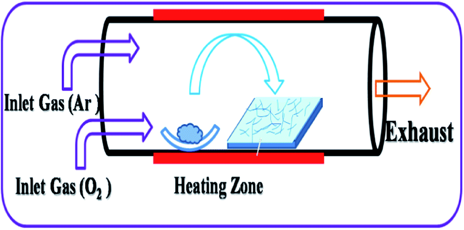
Fig. 1 shows the experimental set up for the deposition of SnO2 NWs. It consists of a horizontal tubular furnace and a mass flow controller. Tin (Sn) powder from Sigma Aldrich (10 μm, 99% trace metals basis) was used as source material for the synthesis of SnO2 NWs. After that Sn powder was loaded in an alumina boat and placed inside the center of the heating zone of the furnace.
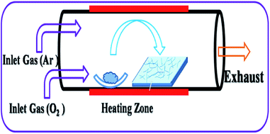 |
| | Fig. 1 Schematic sketch of tubular furnace. | |
A silicon wafer with thickness 380 ± 25 μm, resistivity 1–10 Ω cm, orientation 〈100〉 ± 0.50 (WRS materials USA) was chosen as the substrate. These silicon substrates were placed on the downstream side at a distance of 5 cm (sample S1) and 10 cm (sample S2) from the source materials, and then the furnace was evacuated to 10−2 Torr by using rotary vacuum pump and purged with argon gas at 200 sccm. Then the furnace temperature was raised to growth temperature, i.e. 850 °C. Once the growth temperature was attained high purity oxygen gas with flow rate 50 sccm and the growth process was maintained for 180 minutes. Then the process flow of carrier gases were stopped and the furnace was cooled down to room temperature. These process parameters were tuned such that samples S1 and S2 exhibited a single phase tetragonal microstructure and mixed-phase (R + O) microstructure, respectively. It is found that the morphology of the deposited structure depends on deposition time, substrate temperature, furnace temperature and gas flow rate, however, the existence of O-phase mainly depends on the distance between the source and the substrate position. For sensing measurements, gold pattern electrodes were deposited on the sensing layer and the sensing area, 0.51 cm2, was kept constant for both the sensors S1 and S2. The operating temperature was varied from 50 °C to 350 °C in order to find out the optimum working temperature with varying concentrations of CO gas passed to the sensing chamber using a mass flow controller. Change in resistance of the sensor films was measured as a function of time through a computer interfaced EXTECH MultiMaster™ 560A True RMS digital multimeter. Detailed description of the indigenous sensing setup has already been reported elsewhere.17
2.2 Characterization tools
All the samples were characterized by X-ray diffraction (XRD) using a Bruker AXS, Germany (Model D8 Advanced) diffractometer in the scanning range of 20–80° (2θ) using CuKα radiation (λ = 1.5418 Å). Surface morphology of these deposited nanowires was studied using a Carl Zeiss Field Emission Scanning Electron Microscope (Carl Zeiss AG, Germany). Sensor testing was carried out using the indigenous sensing set up.
3. Results and discussions
3.1 XRD analysis
Fig. 2 displays XRD patterns of S1 and S2 samples. All the Bragg diffraction peaks of S1 can be indexed to the cassiterite (R-rutile) structure of SnO2 with tetragonal lattice parameters a = b = 4.738(1) Å and c = 3.1855(9) Å consistent with ICDD 85-0423, whereas S2 exhibits a few but distinct peaks of orthorhombic (O-) phase (ICDD 78-1063) along with majority R-phase. The volume fraction of O-phase in S2, is estimated by calculating the ratio (IO/IR) of the intensity of the strongest orthorhombic reflection (111) to the intensity of the strongest tetragonal reflection (110),18 revealed that S2 contains 8% of O-phase and 92% of R-phase. Generally the orthorhombic structured SnO2 is formed under high pressures at this temperature.19 Orthorhombic phase formation at moderate temp and low pressure in oxygen deficient atmosphere has also been reported in the literature.19–21
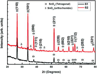 |
| | Fig. 2 XRD pattern of SnO2 NWs deposited at 850 °C (a) 5 cm away (S1) (b) 10 cm away (S2) from the source material. | |
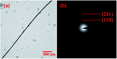
Detailed texture studies based on Harris’s analysis were performed in order to calculate the texture coefficient of R-phase using the relationship:22
| |
 | (1) |
where
P(
hkl) is the texture coefficient of the plane specified by Miller indices (
hkl);
I(
hkl) and
I0(
hkl) are the specimen and standard integrated intensities, respectively, for a given peak and
n is the number of diffraction peaks. Comparison of the texture coefficients of different planes (
Table 1) reveals that for S1, nanowires are highly textured along the (110) plane, which has highest packing fraction of planar density in the rutile structure, useful for sensing, as this plane is effective in electron transfer
via oxygen adions, (mostly O
−).
23 In S2, growth of the (110) plane in R-phase SnO
2 may be restricted due to the presence of O-phase as evidenced by a reduced texture coefficient of the (110) plane in S2 and instead a strong increase in texture along the (200) plane is noticed.
17
Table 1 Texture coefficient of samples S1 and S2
| Sample name |
Planes (hkl) |
Texture coefficient |
| S1 |
110 |
1.926628 |
| 101 |
1.33498 |
| 200 |
0.829961 |
| 211 |
0.474329 |
| 112 |
0.434102 |
| S2 |
110 |
1.007898 |
| 101 |
1.112282 |
| 200 |
1.489113 |
| 211 |
0.667335 |
| 112 |
0.723372 |
3.2 FESEM analysis
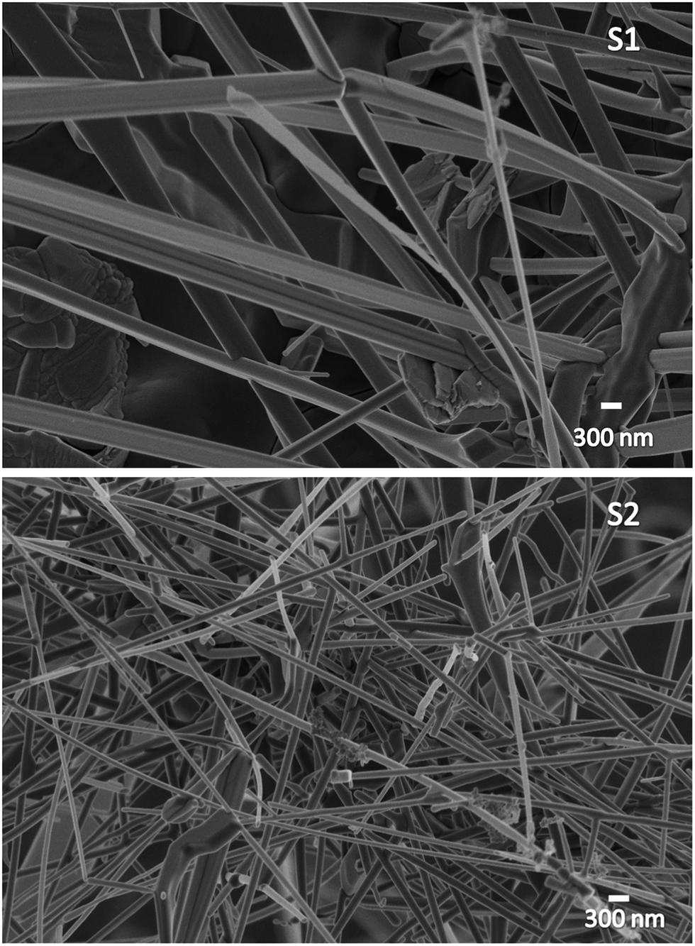
Fig. 3 shows FESEM micrographs of samples S1 and S2. NWs are clearly seen with a large aspect ratio in the range of 40–50.
 |
| | Fig. 3 FESEM micrograph of S1 and S2 sensors. | |
The diameters of the NWs are found to be in the range of 50 to 400 nm with some branchings. The thinnest NWs of 50 nm diameter were grown in sample S2 where as the highest diameter NWs in S1 sample was in the range of 300 to 400 nm. These observations suggest that the thickness of deposited NWs decreases with the distance between the substrate and the source. The NWs in both S1 and S2 showed a very good adhesion with the substrate.
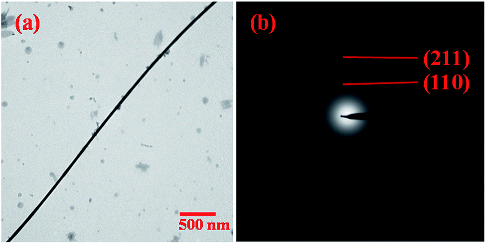
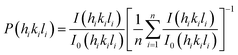
3.3 TEM analysis
TEM imaging of S2 which has mixed phases (O + T) is shown in Fig. 4(a). NWs are of ∼50 nm diameter is observed. The SAD pattern of S2 shown in Fig. 4(b) reveals that NWs have a tetragonal structure with ring patterns observed for the (110) and (211) planes. However, an orthorhombic phase could not be detected owing to its low volume fraction (∼8%) determined by XRD analysis. As TEM is a highly localized probe, as compared to XRD, it was not possible to determine the existence of an orthorhombic SnO2 phase from TEM analysis.
 |
| | Fig. 4 (a) TEM image of S2 NWs sensors, (b) electron diffraction pattern of the nanowires shown in (a). | |
3.4 Sensing measurements
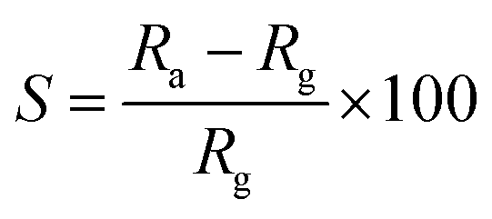
Fig. 5(a) and (b) shows the CO sensing response of samples S1 and S2 at optimum operating temperature under the exposure of different gas concentrations. The gas sensor response is defined as:| |
 | (2) |
where, Rg is the electrical resistance in the presence of CO in air and Ra is the electrical resistance in air. The sensors made of NWs from S1 & S2 were tested at a temperature range from 50 °C to 300 °C.
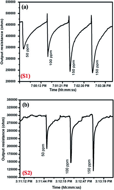 |
| | Fig. 5 Sensor response of (a) S1 for different concentration of CO at 225 °C (b) S2 for different concentration of CO at 175 °C as a function of time. | |
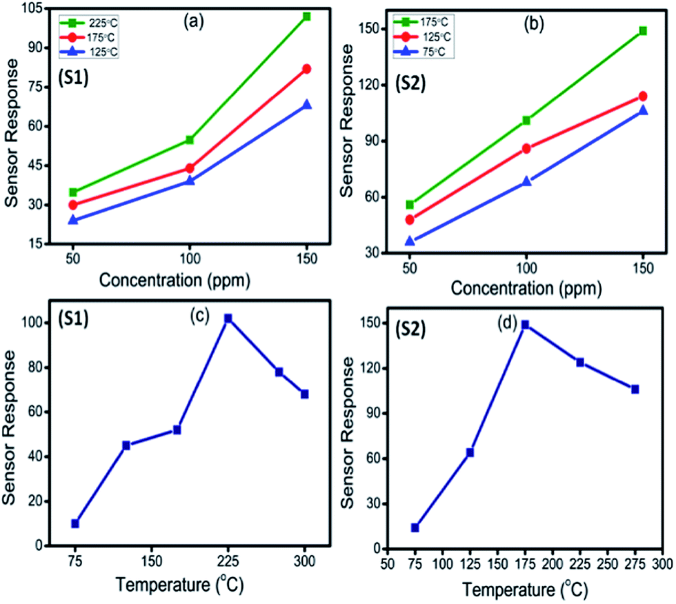
S1 shows a maximum response at 225 °C and S2 shows a maximum response at 175 °C for different concentration of CO. Sensing response of the NWs depends upon the exchange rate of gas, density of charge carriers and hence the temperature. It is observed that for S1 sensor the sensing response is increased with temperature up to 225 °C and then decreased beyond 225 °C for all gas concentrations as shown in Fig. 6(c) and for S2 sensor the sensing response is increased with temperature up to 175 °C and decreased beyond 175 °C for all gas concentrations as shown in Fig. 6(d). From Fig. 5(a) and (b) the measured response- (recovery-) times for S1 are 1–2 s (20–55 s) and for S2 are 1–2 s (15–40 s), respectively.
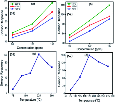 |
| | Fig. 6 Sensor response of S1 and S2 as a function of concentration (a and b) & temperature (c and d). | |
The sensors were capable of detecting CO in the range of 50–150 ppm at temperatures 50 °C to 300 °C and recover quickly once the CO is removed, as shown in Fig. 6 (a) and (b). S1 and S2 NWs exhibit a maximum sensitivity of 102 and 150 for 150 ppm of CO, respectively. These results show that mixed phase NWs with (R + O) structure exhibit higher sensitivity than single (R-) phase NWs. Our results also indicate that a large surface area available due to reduction in diameter of NWs also plays a very important role in the sensitivity of the sensors, which is also supported by literature.24,25 These results are also consistent with texture analysis. Texture coefficients calculated for different Miller planes are tabulated in Table 1. It reveals that as compared to samples S1, the texture coefficient of the (200) plane increased noticeably in S2, at the cost of a decrease in planar density along the (110) plane. Such a change in texture coefficients was reported earlier with dopants like Fe, In and W.17,26 Reduced texture coefficient of a dense (110) plane can act as sink of vacancies and thereby improve sensing response in S2.
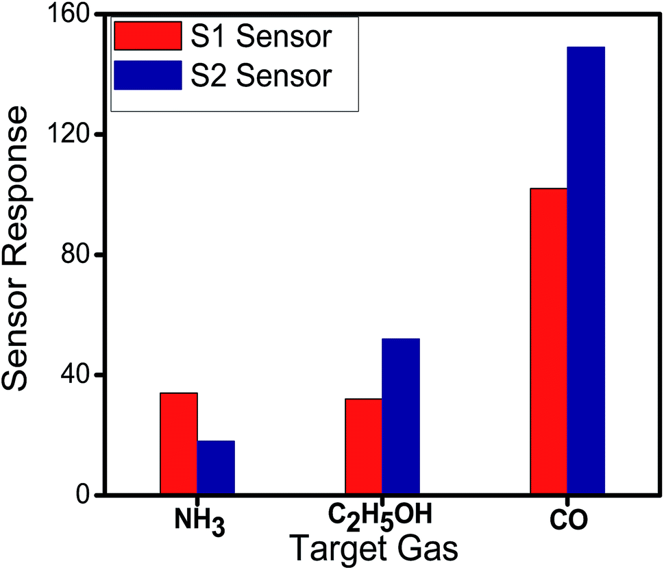
Cross sensitivity behavior of these sensors S1 and S2 was tested with 150 ppm of CO, C2H5OH and NH3 gas, as shown in Fig. 7. It is confirmed from the Fig. 7 that S2 sensor is highly sensitive to CO gas at its working temperature 175 °C. Several literature reports revealed that pure SnO2 is selective for CO at a particular operating temperature.27–29
 |
| | Fig. 7 Sensors response of S1 and S2 sensors for different target gases at 150 ppm. | |
The higher sensor response of S2 sample for CO, as seen in Fig. 7, in the present work, might be due to NWs of smaller diameters, mixed phase and huge reduction in texture coefficient along the most densely packed (110) plane.
4. Conclusions
Preferentially grown tin oxide NWs along the (110) and (200) planes are deposited on a silicon substrate at a deposition temperature of 850 °C. The NWs have an average diameter of 50–350 nm. XRD studies reveal that tetragonal or mixed phase (orthorhombic and tetragonal) SnO2 NWs can be stabilized selectively by changing the distance between source and substrate. TEM studies reveal that 50 nm tin oxide NWs have tetragonal structure. It is found that the texture coefficient, diameter and mixed phase structure of NWs play very important role for sensitivity of the sensors. Sensor response increases with increase in texture coefficient of (200) plane with concurrent decrease in texture coefficient of (110) plane in mixed phase SnO2 NWs. The mixed phase (orthorhombic and rutile) SnO2 NWs with lower diameters (50–200 nm) thus, exhibit enhanced sensitivity for CO detection as compared to single phase.
Acknowledgements
Authors are thankful to Vice Chancellor, Defence Institute of Advanced Technology, Girinagar, Pune-411025 (India) for his support. ACA and MK acknowledges the ER-IPR grant no. ERIP/ER/1003883/M/01/908/2012/D (R&D)/1416 through DRDO-DIAT program on nanomaterials.
References
- N. Kikuchi, E. Kusano, E. Kishio and A. Kinbara, Vacuum, 2002, 6, 365–371 CrossRef.
- Y. Zhao, Q. Zhou, L. Liu, J. Xu, M. Yan and Z. Jiang, Electrochim. Acta, 2006, 51, 2639 CrossRef CAS PubMed.
- J. Seop Lee and J. Jang, J. Ind. Eng. Chem., 2014, 20, 363–371 CrossRef PubMed.
- S. Su, R. Zuo, X. Wang and L. Li, Mater. Res. Bull., 2010, 45, 124–128 CrossRef CAS PubMed.
- Z. Zhu, Appl. Surf. Sci., 2006, 253, 792–796 CrossRef PubMed.
- S. Pilkenton and D. Raftery, Solid State Nucl. Magn. Reson., 2003, 24, 236–253 CrossRef CAS.
- L.-W. Chang, M.-W. Huang, C.-T. Li and H. C. Shih, Appl. Surf. Sci., 2013, 279, 167–170 CrossRef CAS PubMed.
- M. Batzill and U. Diebold, Prog. Surf. Sci., 2005, 79, 47–154 CrossRef CAS PubMed.
- L. Wang, Y. Chen, J. Ma, L. Chen, Z. Xu and T. Wang, Sci. Rep., 2013, 3, 3500, DOI:10.1038/srep03500.
- W. Yang, S. Yu, Y. Zhang and W. Zhang, Thin Solid Films, 2013, 542, 285–288 CrossRef CAS PubMed.
- R. Y. Korotkov, P. Ricou and A. J. E. Farran, Thin Solid Films, 2006, 502, 79–87 CrossRef CAS PubMed.
- G. Korotcenkov, I. Blinov, M. Ivanov and J. R. Stetter, Sens. Actuators, B, 2007, 120, 679–686 CrossRef CAS PubMed.
- X. Zhong, B. Yang, X. Zhang, J. Jia and G. Yi, Particuology, 2012, 10, 365–370 CrossRef CAS PubMed.
- Y. Guan, D. Wang, X. Zhou, P. Sun, H. Wang, J. Ma and G. Lu, Sens. Actuators, B, 2014, 191, 45–52 CrossRef CAS PubMed.
- C. Zheng, X. Zheng, Z. Hong, X. Ding and M. Wei, Mater. Lett., 2011, 65, 1645–1647 CrossRef CAS PubMed.
- S. Tian, Y. Gao, D. Zeng and C. Xie, J. Am. Ceram. Soc., 2012, 95, 436–442 CrossRef CAS PubMed.
- M. Kumar, A. Kumar and A. C. Abhyankar, Ceram. Int., 2014, 40, 8411–8418 CrossRef CAS PubMed.
- R. A. Spurr and H. Myers, Anal. Chem., 1957, 29, 760 CrossRef CAS.
- F. J. Lamelas and S. A. Reid, Phys. Rev. B: Condens. Matter Mater. Phys., 1999, 60, 9347–9352 CrossRef CAS.
- Z. R. Dai, Z. Wei Pan and Z. L. Wang, Adv. Funct. Mater., 2003, 13, 9–24 CrossRef CAS PubMed.
- Z. R. Dai, J. L. Gole, J. D. Stout and Z. L. Wang, J. Phys. Chem. B, 2002, 106, 1274–1279 CrossRef CAS.
- G. B. Harris, Philos. Mag., 1952, 43, 113 CrossRef.
- M. A. Maki-Jaskari and T. T. Rantala, Phys. Rev. B: Condens. Matter Mater. Phys., 2002, 65, 1–6 CrossRef.
- D. Meng, N. M. Shaalan, T. Yamazaki and T. Kikuta, Sens. Actuators, B, 2012, 169, 113–120 CrossRef CAS PubMed.
- N. M. Shaalan, T. Yamazaki and T. Kikuta, Sens. Actuators, B, 2011, 153, 11–16 CrossRef CAS PubMed.
- M. Kumar, A. Kumar and A. C. Abhyankar, ACS Appl. Mater. Interfaces, 2015, 7, 3571–3580 CAS.
- G. Tulzer, S. Baumgartner, E. Brunet, G. C. Mutinati, S. Steinhauer, A. Kock and C. Heitzinger, Procedia Eng., 2012, 47, 809–812 CrossRef CAS PubMed.
- A. M. Gaskov and M. N. Rumyantseva, Inorg. Mater., 2000, 36, 293–301 CrossRef CAS.
- P. G. Harrison and M. J. Willet, Nature, 1998, 332, 337–339 CrossRef.
|
| This journal is © The Royal Society of Chemistry 2015 |
Click here to see how this site uses Cookies. View our privacy policy here.