Electrical characteristics of gallium–indium–zinc oxide thin-film transistor non-volatile memory with Sm2O3 and SmTiO3 charge trapping layers

Jim-Long Hera, Fa-Hsyang Chenb, Ching-Hung Chenb and Tung-Ming Pan*b
aDivision of Natural Science, Center for General Education, Chang Gung University, Taoyuan 333, Taiwan
bDepartment of Electronics Engineering, Chang Gung University, Taoyuan 333, Taiwan. E-mail: tmpan@mail.cgu.edu.tw; Fax: +886-3-2118507; Tel: +886-3-2118800 ext. 3349

Received 1st December 2014 , Accepted 24th December 2014

First published on 24th December 2014


Abstract

In this study, we report the structural and electrical characteristics of high-κ Sm2O3 and SmTiO3 charge trapping layers on an indium–gallium–zinc oxide (IGZO) thin-film transistor (TFT) for non-volatile memory device applications. The IGZO TFT non-volatile memory featuring a SmTiO3 charge trapping layer exhibited better characteristics, including a larger memory window (2.7 V), long charge retention time (105 s with charge loss <15%) and better endurance performance for program/erase cycles (104), compared with a Sm2O3 charge trapping layer. These results can be attributed to the SmTiO3 film possessing a high dielectric constant and deep trapping level. The high-κ SmTiO3 is an excellent candidate for use as the trapping layer in IGZO TFT non-volatile memories.

Introduction

Amorphous indium–gallium–zinc oxide (IGZO) is widely investigated as a channel material in thin-film transistors (TFTs) for flat, flexible and transparent display applications due to its high field mobility, wide band gap, good uniformity, high transparency, and low processing temperature.1,2 To develop the next-generation system-on-panel (SOP) applications, IGZO TFT nonvolatile memories have been studied as a TFT switch and memory element.3–7 Various IGZO TFT memories with different charge storage media such as, metal nanocrystals (Pt, Au)4,5 and dielectrics (SiOx, Si3N4, Al2O3),6,7 are explored. However, the high operating voltages, retention loss and cycling decay are the challenges. To obtain high erasing efficiency, a large number of holes must be generated in the IGZO channel during an erasing operation. Several methods, such as light irradiation8 and light-assisted negative-gate-bias erasing,9 have been proposed to improve the erasing efficiency of IGZO TFT memory. However, the addition of instrument of an ultraviolet light is required during the erasure process. In order to address this issue, high-κ dielectric materials have been studied as a charge trapping layer for silicon-oxide-high-κ-oxide-silicon-type memories without decreasing the thickness of tunneling oxide.10,11 Previously, it has been proved that the Ti-doped HfO2 (HfTiO) high-κ dielectric has better material and electrical properties than the un-doped HfO2 film, such as the thinner interfacial layer, higher κ value and lower leakage current.12,13

Recently, rare-earth (RE) oxide films are considered to be suitable materials for further scaling of nonvolatile memory devices because of their promising thermal stability and better electrical properties.14,15 Among RE oxide materials, thin Sm2O3 film is one of the most potential candidates as a charge trapping layer for nonvolatile memory applications due to its high dielectric constant of 15, wide energy bandgap of 4.33 eV and high breakdown electric field of 7 MV cm−1.15–17 However, the formation of hydroxide film is found at the surface of RE oxide due to high hygroscopicity.18 To avoid this problem, the high stability properties of RE oxide film can be realized by the addition of Ti atoms into the RE film.19 In our previous research results showed that the incorporation of Ti into RE oxide films exhibited excellent electrical characteristics including a high dielectric constant, a low leakage current and a large breakdown voltage.20 In this paper, we compared the high-κ Sm2O3 and SmTiO3 films as a charge trapping layer in metal-oxide-high-κ-oxide-IGZO (MOHOI) nonvolatile memory based on TFT device. The film structure and composition of high-κ Sm2O3 and SmTiO3 films were analyzed by X-ray diffraction (XRD) and X-ray photoelectron spectroscopy (XPS), respectively. The electrical characteristics of high-κ Sm2O3 and SmTiO3 MOHOI-type TFT nonvolatile memories are also investigated.

Experimental

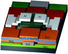
Inverted staggered IGZO TFT nonvolatile memory devices with high-κ Sm2O3 and SmTiO3 charge trapping layers were processed on SiO2/Si substrate as shown in Fig. 1. A TaN (40 nm) was deposited as a bottom gate electrode by reactive sputtering at room temperature. A SiO2 (50 nm) blocking layer was deposited on the bottom gate electrode, followed by a 40 nm Sm2O3 or SmTiO3 charge trapping layer and a 8 nm SiO2 tunneling layer. The blocking layer and tunneling layer were deposited through rf sputtering using a SiO2 target. Next, the Sm2O3 charge trapping layer was deposited by rf sputtering using a Sm target in Ar/O2 ambient, whereas the SmTiO3 charge trapping layer was deposited through rf cosputtering using both Sm and Ti targets. All samples were annealed at 400 °C in O2 ambient for 10 min. Then, a 20 nm channel layer was deposited by means of rf sputtering using an IGZO target (In2O3[thin space (1/6-em)]:[thin space (1/6-em)]Ga2O3[thin space (1/6-em)]:[thin space (1/6-em)]ZnO = 1[thin space (1/6-em)]:[thin space (1/6-em)]1[thin space (1/6-em)]:[thin space (1/6-em)]1 in mol ratio) at room temperature. The post-deposition annealing was performed in N2 ambient for 1 h at 200 °C. Finally, the patterned Al layer (∼50 nm) as the source and the drain electrodes was deposited using the thermal evaporation technique, followed by a typical lift-off process. The channel width and length of the fabricated TFTs were 100 μm and 10 μm, respectively.
image file: c4ra15538f-f1.tif
Fig. 1 Schematic structure of the IGZO TFT nonvolatile memory with a high-κ Sm2O3 or SmTiO3 charge trapping layer.

The crystalline structure and the chemical composition of the dielectric films were investigated using XRD and XPS analyses, respectively. XRD analysis was performed using a Bruker-AXS D5005 diffractometer with a Cu Kα (λ = 1.542 Å) radiation. The chemical bonding of the dielectric was determined using a monochromatic Al Kα (1486.7 eV) source. The transfer characteristics (drain current–gate voltage, IDSVGS) of the high-κ Sm2O3 and SmTiO3 IGZO TFT nonvolatile memories were measured by an Agilent 4156C semiconductor parameter analyzer. The threshold voltage (VTH) of TFT nonvolatile memories was defined as the VGS at which the IDS reaches 0.1 nA for a drain voltage of 1 V.

Results and discussion

Fig. 2(a) displays the XRD pattern of the Sm2O3 and SmTiO3 thin films after 400 °C annealing in O2 ambient. Three strong (222), (400) and (440) peaks and one weak (622) peak were found in the Sm2O3 film. In contrast, for the SmTiO3 sample, a large (200) reflection peak and four small (021), (221), (311), and (132) reflection peaks are observed in the 2θ diagram. These dielectric films are belong to polycrystalline structures. Fig. 2(b) and (c) show the Sm 3d and O 1s XPS spectra of the Sm2O3 and SmTiO3 films, respectively. Fig. 2(b) depicts that the binding energy of Sm 3d5/2 and 3d3/2 double peaks is located at 1083.1 eV and 1110.1 eV, respectively, for the Sm2O3 film.21 The Sm 3d double peaks (Sm 3d5/2 at 1083.6 eV and Sm 3d3/2 at 1110.6 eV) for the SmTiO3 film shift to higher binding energy by 0.5 eV relative to those for the Sm2O3. This shift can be related to the reaction of TiOx with the Sm atom to form a SmTiO3 structure. The O 1s spectra of the Sm2O3 and SmTiO3 films are shown in Fig. 2(c) with their appropriate peak curve-fitting lines. The O 1s signal of Sm2O3 film comprised three peaks: one peak for Sm–O boding at 529.2 eV,21 one for oxygen vacancy at 530.9 eV (ref. 22) and one for Sm–OH bonding at 532.1 eV.23 The intensity of the O 1s peak corresponding to Sm(OH)x was larger than that of Sm2O3. This result can be attributed to the oxygen vacancies in the Sm2O3 film leading to the moisture absorption property exposed to the air.18 Furthermore, the SmTiO3 film also comprised three peaks at 529.2, 530 and 531.3 eV, which we can assign to Sm–O binding, Sm–O–Ti binding24 and oxygen vacancy,25 respectively. The O 1s peak corresponding to SmTiO3 exhibits a larger intensity peak compared with Sm2O3. This result indicates that the reaction of TiOx with Sm atom form a SmTiO3 structure reducing the formation of a Sm2O3 film.
image file: c4ra15538f-f2.tif
Fig. 2 (a) XRD pattern of the Sm2O3 and SmTiO3 dielectric films. XPS spectra of (b) Sm 3d and (c) O 1s for Sm2O3 and SmTiO3 dielectric films.

Fig. 3 shows the transfer (IDSVGS) characteristics of the MOHOI-type TFT nonvolatile memories with Sm2O3 and SmTiO3 charge trapping layers before and after programming voltage at 15 V for 100 ms. The κ value of Sm2O3 and SmTiO3 dielectric films was determined to be 8.6 and 11, respectively, from capacitance–voltage curve. The IGZO TFT nonvolatile memory with a SmTiO3 charge trapping layer has a larger memory window (2.7 V) than that with Sm2O3 charge trapping layer (1.7 V). The IGZO is a natural n-type semiconductor that generally only supplies electrons for charge transport in the channel. During electrical programming, electrons from the a-IGZO channel can be easily trapped in the SmTiO3 by Fowler–Nordheim (F–N) tunneling. The high dielectric constant of SmTiO3 film increased the effective electric field across the tunneling oxide, thus enhancing more electrons trapped in the SmTiO3 film. The effective electric field across the SiO2 tunneling layer in Sm2O3 and SmTiO3 IGZO TFT memories was estimated to be 1.97 and 2.08 MV cm−1, respectively.


image file: c4ra15538f-f3.tif
Fig. 3 Transfer characteristics of the MOHOI-type TFT nonvolatile memories with Sm2O3 and SmTiO3 charge trapping layers.

Fig. 4(a) and (b) illustrate the band diagram of the SmTiO3 IGZO TFT memory device after the programming and erasing operation, respectively. When the positive voltage pulse was applied for the program state, as shown in Fig. 4(a), the electrons accumulated in the IGZO channel were transferred into the SmTiO3 trap layer. Therefore, the VTH is shifted to the positive direction. At this state, it can be expected that most electrons trapped in the SmTiO3 trap layer were located in deep level states, because shallow levels of SmTiO3 were mostly filled with inherent electrons.26 The electrons should pass through the shallow level states to the deep level states. A large number of electrons located in the shallow level states of SmTiO3 could act as some self-limiting elements due to their same polarity. Furthermore, for the case of erasing state shown in Fig. 4(b), the electrons accumulated in shallow levels can be firstly transported to the IGZO channel and the electrons trapped in deep levels are subsequently detrapped. Then, the required erase time for the erasing operation, which was involved with the trapping event into the deep levels of SmTiO3, may be longer than that for the program state, which was related to the charge transfer from the shallow levels of SmTiO3.


image file: c4ra15538f-f4.tif
Fig. 4 Schematic illustration of band diagram of the SmTiO3 IGZO TFT nonvolatile memory when the (a) positive and (b) negative bias applied to the gate electrode. The channel electrons is indicated as blue circles, whereas inherent electrons of SmTiO3 located in shallow level states and deep level states are green circles and red circles, respectively. The probability of charge trap or detrap is described as size of arrow.

Fig. 5(a) illustrates the ΔVTH values of the SmTiO3 MOHOI-type TFT memory device as a function of the programming time under various gate voltage stresses, where drain and source are grounded. The ΔVTH is defined as the change in threshold voltage between the virginal and programmed states. The F–N tunneling programming and erasing were used for high-κ SmTiO3 IGZO TFT nonvolatile memory operations. We find that the ΔVTH value increases with increasing the programming time. The amount of electrons, which are responsible for the shift of the VTH, trapped in the SmTiO3 layer during the programming process is a function of the programming time, and hence it increases with increasing the programming time. In addition, program voltage was increased, memory window was also increased. After the programming condition of VGS = 15 V at 100 ms, the SmTiO3 IGZO TFT memory device exhibits a large memory window of 2.7 V. The energy bandgap of SmTiO3 film could be decreased by the incorporation of Ti into the Sm2O3.27 This bandgap narrowing gives rise to a large conduction band offset to the trapping layer that facilitates the trapping of the electrons. The SmTiO3 layer was employed to store the high density of injected electrons from the IGZO active layer, causing a large threshold voltage shift. Fig. 5(b) displays the ΔVTH value of the SmTiO3 IGZO TFT memory device as a function of the erasing time under different gate voltage stresses (drain and source are grounded). The gate voltage-dependent erasing characteristics are investigated with a fixed erasing time of 100 ms. The ΔVTH decreases from −2.1 to −2.7 V as the erasing voltage decreases from −9 to −15 V, respectively.


image file: c4ra15538f-f5.tif
Fig. 5 Threshold voltage shift of the SmTiO3 MOHOI-type TFT nonvolatile memory as a function of the (a) programming time (b) erasing time.

Fig. 6(a) shows the data retention characteristics of the Sm2O3 and SmTiO3 MOHOI-type TFT memory devices measured at room temperature. In the programming state, the IGZO TFT memory device using a SmTiO3 film has a lower charge loss (<15%) than that with a Sm2O3 film, measured at 105 s. The addition of Ti into the Sm2O3 created more deep trapping level in the SmTiO3. The trapping electrons transferred readily from shallow level to adjacent deeper level by lateral hopping.28 Therefore, the good data retention characteristic can be related to the most of trapped charges are trapped in the deep trap states of SmTiO3 dielectric. In the erasing state, there is almost no change in the VTH with time. Fig. 6(b) displays the endurance characteristics of the Sm2O3 and SmTiO3 MOHOI-type TFT memory devices under programming condition: VGS = 15 V for 100 ms and erasing condition: VGS = −15 V for 100 ms. The IGZO TFT memory device featuring a SmTiO3 film exhibited better endurance characteristics compared with Sm2O3 film. A slight memory window narrowing occurred and individual threshold voltage shifts become visible in the program and erase states after 100 cycles. This behaviour may be attributed to a large number of storage charges causing the defects in the tunnel oxide during charge transportation process.29 Another possible reason for narrowing of the memory window is that the IGZO film itself is sensitive to the atmosphere and becomes unstable under long time exposure to air or electrical field stressing.30 The trapped charge in the trapping layer easily escapes because of the film variation or is neutralized by the charges in the gate dielectric and gate-dielectric/channel interface.31 After 104 program/erase (P/E) cycles, the memory window of SmTiO3 MOHOI-type TFT memory is still fixed around 2.2 V.


image file: c4ra15538f-f6.tif
Fig. 6 (a) Charge retention and (b) endurance characteristics for the Sm2O3 and SmTiO3 MOHOI-type TFT nonvolatile memories.

The important device parameters of MOHOI-type TFT memory devices are listed in Table 1, where the data from IGZO TFT memory devices using SiO2/IGZO/SiO2,31 Al2O3/IGZO/Al2O3,32 HfLaO/HfON/HfLaO,33 SiO2/Sm2O3/SiO2, and SiO2/SmTiO3/SiO2 stacked structures are listed for comparison. Although our SiO2/SmTiO3/SiO2 TFT memory has a low memory window and a high P/E voltage, it exhibits good data retention and endurance.

Table 1 Comparison of electrical characteristics for IGZO TFT memory devices fabricated with SiO2/IGZO/SiO2, Al2O3/IGZO/Al2O3, HfLao/HfON/HfLao, SiO2/Sm2O3/SiO2, and SiO2/SmTio3/SiO2 stacked structures
Gate stacks Memory window (V) P/E voltage (V) and time (ms) Charge loss (105 s) P/E cycles
SiO2/IGZO/SiO2 5.6 P: VG = 18 for 10 NA NA
E: VG = −23 for 100
Al2O3/IGZO/Al2O3 3.8 P: VG = 14 for 10 >30% 103
E: VG = −14 for 10
HfLaO/HfON/HfLaO 1.2 P: VG = 8 for 1 >60% 102
E: VG = −8 for 0.1
SiO2/Sm2O3/SiO2 1.7 P: VG = 15 for 100 >20% 103
E: VG = −15 for 100
SiO2/SmTiO3/SiO2 2.7 P: VG = 15 for 100 <15% 104
E: VG = −15 for 100


Conclusions

In this paper, we compared the MOHOI-type TFT nonvolatile memory device with high-κ Sm2O3 and SmTiO3 films as a charge trapping layer. The SmTiO3 IGZO TFT nonvolatile memory exhibited a larger memory window (2.7 V), smaller charge loss (<15% after 105 s) and better endurance performance (∼2.2 V after 104 P/E cycles), compared with Sm2O3 IGZO TFT memory. These results are attributed to the SmTiO3 structure with a high dielectric constant and the formation of deep trap states, resulting in the high probability for trapping the charge carrier. The high-κ SmTiO3 MOHOI-type TFT nonvolatile memory device is considered as a promising candidate for SOP applications.

Acknowledgements

This work was supported by the National Science Council, Taiwan, Republic of China, under contract no. NSC-101-2221-E-182-059 and NSC-102-2221-E-182-072-MY3.

References

  1. K. Nomura, H. Ohta, A. Takagi, T. Kamiya, M. Hirano and H. Hosono, Nature, 2004, 432, 488 CrossRef CAS PubMed.
  2. J. Y. Kwon, K. S. Son, J. S. Jung, T. S. Kim, M. K. Ryu, K. B. Park, B. W. Yoo, J. W. Kim, Y. G. Lee, K. C. Park, S. Y. Lee and J. M. Kim, IEEE Electron Device Lett., 2008, 29, 1309 CrossRef CAS.
  3. S. Chen, W. P. Zhang, X. M. Cui, S. J. Ding, Q. Q. Sun and W. Zhang, Appl. Phys. Lett., 2014, 104, 103504 CrossRef PubMed.
  4. J. Jang, J. C. Park, D. Kong, D. M. Kim, J. S. Lee, B. H. Sohn, I. H. Cho and D. H. Kim, IEEE Trans. Electron Devices, 2011, 58, 3940 CrossRef CAS.
  5. A. Suresh, S. Novak, P. Wellenius, V. Misra and J. F. Muth, Appl. Phys. Lett., 2009, 94, 123501 CrossRef PubMed.
  6. H. H. Nguyen, V. D. Nguyen, T. T. Trinh, K. Jang, K. Baek, J. Raja and J. Yi, J. Electrochem. Soc., 2011, 158, H1077 CrossRef CAS PubMed.
  7. J. S. Jung, S. H. Rha, U. K. Kim, Y. J. Chung, Y. S. Jung, J. H. Choi and C. S. Hwang, Appl. Phys. Lett., 2012, 100, 183503 CrossRef PubMed.
  8. S. Chen, X. M. Cui, S. J. Ding, Q. Q. Sun, T. Nyberg, S. L. Zhang and W. Zhang, IEEE Electron Device Lett., 2013, 34, 1008 CrossRef CAS.
  9. T. T. Trinh, V. D. Nguyen, H. H. Nguyen, J. Raja, J. Jang, K. Jang, K. Baek, V. A. Dao and J. Yi, Appl. Phys. Lett., 2012, 100, 143502 CrossRef PubMed.
  10. T. H. Hsu, H. C. You, F. H. Ko and T. F. Lei, J. Electrochem. Soc., 2006, 153, G934 CrossRef CAS PubMed.
  11. T. M. Pan and W. W. Yeh, IEEE Trans. Electron Devices, 2008, 55, 2354 CrossRef CAS.
  12. C. Ye, H. Wang, J. Zhang, Y. Ye, Y. Wang, B. Wang and Y. Jin, J. Appl. Phys., 2010, 107, 104103 CrossRef PubMed.
  13. M. Liu, L. D. Zhang, G. He, X. J. Wang and M. Fang, J. Appl. Phys., 2010, 108, 024102 CrossRef PubMed.
  14. Y. H. Lin, C. H. Chien, T. Y. Yang and T. F. Lei, J. Electrochem. Soc., 2007, 154, H619 CrossRef CAS PubMed.
  15. T. M. Pan and F. H. Chen, Semicond. Sci. Technol., 2011, 26, 045004 CrossRef.
  16. V. A. Rozhkov, A. Y. Trusova and I. G. Berezhnoy, Thin Solid Films, 1998, 325, 151 CrossRef CAS.
  17. H. Yang, H. Wang, H. M. Luo, D. M. Feldmann, P. C. Dowden, R. F. Depaula and Q. X. Jia, Appl. Phys. Lett., 2008, 92, 062905 CrossRef PubMed.
  18. Y. Zhao, M. Toyama, K. Kita, K. Kyuno and A. Toriumi, Appl. Phys. Lett., 2006, 88, 072904 CrossRef PubMed.
  19. R. B. van Dover, Appl. Phys. Lett., 1999, 74, 3041 CrossRef CAS PubMed.
  20. T. M. Pan, L. C. Yen, C. C. Huang and W. C. Lin, Electrochem. Solid-State Lett., 2009, 12, G27 CrossRef CAS PubMed.
  21. Y. A. Teterin and A. Y. Teterin, Russ. Chem. Rev., 2002, 71, 347 CrossRef CAS PubMed.
  22. S. H. Hwang, J. Song, Y. Jung, O. Y. Kweon, H. Song and J. Jang, Chem. Commun., 2011, 47, 9164 RSC.
  23. S. Jeon and H. Hwang, J. Appl. Phys., 2003, 93, 6393 CrossRef CAS PubMed.
  24. J. F. Moulder, W. F. Stickle, P. E. Sobol and K. D. Bomben, Handbook of X-Ray Photoelectron Spectroscopy: A Reference Book of Standard Spectra for Identification and Interpretation of XPS Data, Physical Electronics, Chanhassen, MN, 1995 Search PubMed.
  25. Y. Jeong, C. Bae, D. Kim, K. Song, K. Woo, H. Shin, G. Cao and J. Moon, ACS Appl. Mater. Interfaces, 2010, 3, 611 Search PubMed.
  26. J. Y. Bak, M. K. Ryu, S. H. K. Park, C. S. Hwang and S. M. Yoon, IEEE Trans. Electron Devices, 2014, 61, 2404 CrossRef CAS.
  27. L. Fleming, C. C. Fulton, G. Lucovsky, J. E. Rowe, M. D. Ulrich and J. Luning, J. Appl. Phys., 2007, 102, 033707 CrossRef PubMed.
  28. T. S. Chen, K. H. Wu, H. Chung and C. H. Kao, IEEE Electron Device Lett., 2004, 25, 205 CrossRef CAS.
  29. W. R. Chen, T. C. Chang, J. L. Yeh, S. M. Sze and C. Y. Chang, Appl. Phys. Lett., 2008, 92, 152114 CrossRef PubMed.
  30. D. Kang, H. Lim, C. J. Kim, I. Song and J. G. Chung, Appl. Phys. Lett., 2007, 90, 192101 CrossRef PubMed.
  31. M. F. Hung, Y. C. Wu, J. J. Chang and K. S. Chang-Liao, IEEE Electron Device Lett., 2013, 34, 75 CrossRef CAS.
  32. H. Yin, S. Kim, H. Lim, Y. Min, C. J. Kim, I. Song, J. Park, S. W. Kim, A. Tikhonovsky, J. Hyun and Y. Park, IEEE Trans. Electron Devices, 2008, 55, 2071 CrossRef CAS.
  33. N. C. Su, S. J. Wang and A. Chin, IEEE Electron Device Lett., 2010, 31, 201 CrossRef CAS.

This journal is © The Royal Society of Chemistry 2015
Click here to see how this site uses Cookies. View our privacy policy here.