
 Open Access Article
 This Open Access Article is licensed under a Creative Commons Attribution-Non Commercial 3.0 Unported Licence
Micropatterning of nanoenergetic films of Bi2O3/Al for pyrotechnics
Vinay Kumar
Patel
,
Anurup
Ganguli
,
Rishi
Kant
and
Shantanu
Bhattacharya
*
Microsystems Fabrication Laboratory, Department of Mechanical Engineering, Indian Institute of Technology Kanpur, Kanpur 208016, Uttar Pradesh, India. E-mail: bhattacs@iitk.ac.in; Fax: +91 5122597408; Tel: +91 5122596056
First published on 13th January 2015
Abstract
Initiatives have been led by researchers all around the world to deposit and pattern nanoenergetic films (nEFs) using various techniques so that printed energetic circuits can be developed for initiation of detonation. In the first stage of a similar initiative, Bi2O3 nano-square tablets (NSTs) with an edge length of ca. 200–300 nm and thickness of ca. 50–100 nm were synthesized on gold-sputtered silicon substrates by a chemical bath deposition process. Gold nanofilms on Si-substrates were found to act as catalytic agents for stable colloidal growth of Bi2O3 NSTs. In the absence of a gold catalyst, micro-leaf-shaped structures of Bi2O3 were observed to form using the same process. The developed Bi2O3 NSTs were sputter-coated with aluminum to produce nEFs on the Si-substrate. The exothermic reactivity of Bi2O3/Al nEFs was evaluated at three different aluminum-sputtering thicknesses of 60, 100 and 140 nm, respectively, by TG-DSC measurements taken from 50 to 800 °C at a heating rate of 10 °C min−1 under nitrogen. The nEF formed with 140 nm aluminum sputtering developed the highest heat of reaction, 710 J g−1, at an initiation temperature of 535 °C; when burnt in a constant-volume pressure-cell, this nEF developed a peak pressure of 40.8 MPa and a pressurization rate of 4.08 MPa μs−1. Furthermore, it was possible to pattern the Bi2O3/Al nEFs on Si-substrates up to a resolution of ∼5 microns. The high heat of reaction, low initiation temperature and excellent pressure–time characteristics of the nEFs, and their high-resolution micropatterning on Si-substrates make them useful for pyrotechnics.
I. Introduction
Nanoenergetic materials comprising nanoscale homogeneous mixtures of an oxidizer (CuO,1,2 Bi2O3,1 WO3,1 MoO3,1etc.) and metal fuel (Al) are of significant importance in the development of pyrotechnics, propellants and explosives. Properties such as the ability to be deposited on flat substrates and patternability are of great significance for these materials because they enable some of them to be used in the development of safe Si-based initiator chips for the timed detonation of safe arm and fire devices, etc.3 Nanoenergetic materials react exothermally to convert their chemical energy into mechanical and thermal energy, thus producing high-speed self-propagating combustion reactions and also shock waves if coupled to a suitable medium.4 Packed or patterned nanoenergetic materials are suitably utilized in various applications such as safe arm and fire devices,3 microthrusters5 molecular gene delivery6 as well as pyrotechnic microinitiators.7 Such applications can be easily realized by integrating patterned nanoenergetic materials with CMOS technology. Basically, aluminum is used as a fuel particle in combination with several metal oxides such as CuO,7,8 NiO,9 and Co3O4 (ref. 10) to realize nanoenergetic behavior. The oxidizer nanostructures of CuO/NiO/Co3O4 on MEMS devices have previously been fabricated by controlled oxidation of as-deposited Cu/Ni/Co thin films, although most of this technology is confined to only one dimension (thickness), being on the nanometer scale.7–10 The power of stand-alone nanostructuring using molecular self-assembly processes to achieve an overall nano-size for the participating fuel and oxidizers has been explored by many groups. Bi2O3/Al-based micro-chip initiators were reported recently,11 in which Bi2O3 and aluminum nanoparticles were mixed externally and packaged on micro-chips, which requires state-of-the-art packaging methodology to retain the nanoenergetic composites with micro-chips. However, there were serious issues regarding the ability of such as-grown materials to bind to the microchip surface during patterning. Furthermore, any ligand molecule used in patterning of the surfaces would itself affect the rate of burning and the explosive performance of the nanoenergetic materials.Bismuth oxide (Bi2O3) is a narrow-bandgap (2.8 eV) dielectric material having excellent electrical,12 optical,13 conducting14 and catalytic15 properties. A few developments have been reported regarding the synthesis of bismuth oxide nanostructures on glass substrates using chemical bath deposition16 and on Au-coated silicon substrates using atmospheric chemical vapor deposition,17 the thermal evaporation of bismuth oxide powder in a horizontal tube furnace under argon flow,18etc. These developments inspired us to utilize the available knowledge to formulate nano-square tablets of bismuth oxide using a noble metal (Au in our case) as a catalytic agent followed by chemical bath deposition of Bi2O3. The catalytic behavior of such noble metals is well known and is principally due to enhanced interfacial charge transfer.19 The nanoenergetic composite films of Bi2O3/Al were prepared by sputter deposition of aluminum on a previously grown Bi2O3 nanotablet substrate, using optimized deposition conditions. The exothermic reactivity of the as-prepared nanoenergetic films were examined by TG-DSC analysis from 50 to 800 °C in a nitrogen atmosphere.
II. Experimental section
A. Preprocessing of silicon substrates
A 500 μm-thick silicon (p-type) wafer polished on both sides was sonicated for 30 min in acetone followed by rinsing for 15 min with 2-propanol. The wafer was further rinsed in deionized (DI) water and blow-dried with laboratory-grade nitrogen gas, followed by heating in a vacuum oven at 60 °C for 2 hours. A thin layer of insulating SiO2 was grown on the cleaned silicon substrate at 1000 °C by the wet oxidation technique using a batch top furnace (MRL Industries). The thickness of the as-grown SiO2 layer (1 micron layer-thickness) corresponding to a growth time of 4 hours was measured using Nanocalc (Ocean Optics).B. Laser micromachining of the PMMA mask
A polymethylmethacrylate (PMMA) mask was micromachined with a CO2 pulse laser (M/S Epilog laser, USA). The design of the intended micropattern was carried out using Corel Draw. The drawing data were converted into a data exchange format which was used to drive the various stepper motors of the laser machine and all motions were confined to the x–y plane. The laser machining was performed at room temperature under atmospheric pressure. The micromachining using the laser was carried out on a 1 mm-thick PMMA sheet at a laser speed scanning rate (vector mode) of 15 mm s−1, a laser power of 35 watt and laser frequency of 5 kHz. In addition, wet chemical etching was performed on the laser-cut samples with a mixture of acetone and ethanol at a ratio of 1![[thin space (1/6-em)]](https://www.rsc.org/images/entities/char_2009.gif) :2 in an ultrasonic bath set to a frequency of 42 kHz for 20 minutes. This procedure helped us to achieve a high cut-edge quality of the micromachined mask surface and edges.
:2 in an ultrasonic bath set to a frequency of 42 kHz for 20 minutes. This procedure helped us to achieve a high cut-edge quality of the micromachined mask surface and edges.
C. PMMA masking of Si-substrate
A thin layer of sacrificial polydimethylsiloxane (PDMS) was spin coated on a glass slide for about 8–9 minutes at 8000 rpm using a spin coater (M/S SPS-BV, Netherlands). The PDMS was prepared by mixing the prepolymers (M s−1 Dow Corning, Midland) in a ratio of 10:1 by weight with a curing agent. The bottom surface of the mask was stamped onto this coated PDMS for about 5 seconds and a thin layer (∼1–2 μm) of PDMS then became sheared from the parent film and adhered to the PMMA mask as the mask was separated from the parent film. This PDMS is tacky, which facilitates this layer transfer process. This layer is used as an adhesive and is sandwiched between the mask and the silicon substrate onto which the mask is superimposed. This assembly was cured at 90 °C for about 15 min, which resulted in tight bonding between the mask and the substrate. We further performed a leak test on this assembly by pouring a red dye and observing the optical patterns with an optical microscope (Nikon 80i).
D. Synthesis of Bi2O3 NSTs and realization of nEFs
The SiO2-layered substrates with and without the PMMA mask were sputter coated with a 2 nm layer of titanium using an NSP4000 dual chamber sputtering-PECVD system (Nanomaster Inc.). The sputtered layer was obtained at 160 W power, an argon pressure of 2.5 mTorr and an argon flow rate of 20 sccm. The sputtering was further followed by another gold layer with a thickness of 5 nm as a stack (sputtering power of 200 W, argon flow rate of 20 sccm and pressure of 8 mTorr). Bismuth oxide nano-square tablets were prepared by successive dipping of the Au-coated silicon substrate in two separate precursor solutions for 15 seconds followed by rinsing with water between the dipping steps. The first precursor solution contained bismuth hydroxyl ions at pH 10; it was prepared by adding 0.1 mol of bismuth nitrate into a solution containing 5 ml of concentrated (70%) nitric acid and 95 ml of deionised water, followed by drop-by-drop addition of NaOH. The second precursor solution, containing hydrogen ions, consisted of 1% hydrochloric acid. The first precursor solution was magnetically stirred throughout the deposition process and fresh deionised water was used after each cycle of deposition. The Bi2O3/Al nEFs were prepared by sputter deposition of aluminum onto the as-prepared Bi2O3 NSTs under an argon pressure of 5 mTorr and an argon flow rate of 20 sccm at a sputtering power of 200 W. The sputtering layer (Ti/Au/Al) thickness was measured using the thickness monitor of the sputtering-PECVD system, NSP4000.E. Material characterization
The structural morphologies of as-prepared Bi2O3 NSTs and Bi2O3/Al nEFs on Au-sputtered Si substrate were characterized by field-emission scanning electron microscopy (Supra 40 VP, Zeiss Germany), and by powder X-ray diffraction using an X'Pert Pro diffractometer (PANanalytical, Netherlands) in the 2θ range of 20–70°, at a scan rate of 0.02 s−1 with Cu Kα radiation of wavelength 1.5418 Å. The Bi2O3 NSTs on the silicon substrate was characterized by FT-IR spectroscopy over the wave number range from 400 cm−1 to 4000 cm−1 using a Perkin-Elmer Spectrum spectrometer. The mass changes and heats of reaction of Al-sputtered Bi2O3 NSTs were characterized using thermogravimetry and differential scanning calorimetry (TG-DSC) studies carried out on a Netzsch STA 449F3 instrument. The TG-DSC analysis was carried out from 50 to 800 °C at a heating rate of 10 °C min−1, under nitrogen gas (99.999% purity) flowing at 20 ml min−1.The pressure and the pressurization rate of the nanoenergetic composites were measured by conducting a combustion experiment using 15 mg of Bi2O3/nAl composites in a constant-volume pressure-cell (diameter = 6.25 mm, depth = 2.5 mm) as shown in Fig. 1. A piezoelectric pressure sensor PCB 119B12 (PCB Piezotronics) was rigidly fixed to the pressure-cell to measure the pressure–time characteristics of the combustion, which were recorded using a Tektronix digital oscilloscope (DPO3054).
 | ||
| Fig. 1 Pressure–time characteristics measurement setup. | ||
III. Results and discussion
X-ray diffraction patterns of as-grown Bi2O3 NSTs on a gold-coated Si substrate with stacked aluminum are shown in Fig. 2. The XRD pattern is consistent with monoclinic bismuth oxide of the JCPDS standard (41-1449), as seen in Fig. 1, and peaks corresponding to titanium and gold, but not to hydroxide, were also detected in the XRD. The EDX measurements of nanoenergetic films are shown in Fig. 3. Here, peaks corresponding to the elements Ti, Au and Al are clearly seen, which is consistent with the XRD measurements in Fig. 2. The morphology and structure of as-synthesised bismuth oxide on bare as well as Au-sputtered Si substrates were studied by FESEM. It was observed that a micro-leaf-like structure of bismuth oxide could be formed on bare silicon substrates as shown in Fig. 4(a). Substrates with Ti/Au stacks showed the formation of bismuth oxide nano-square tablets, which did not arise in the absence of the Au/Ti stack. This observation is strongly consistent with the indicated formations. Fig. 4(b) and (c) show the formation of nano-square tablets of bismuth oxide on Au-sputtered Si-substrate with an average edge length of 200–300 nm and thickness of 50–100 nm. Fig. 4(d) shows the FESEM image of nanoenergetic films of Bi2O3 NSTs with sputtered-aluminum of thickness around 100 nm. | ||
| Fig. 2 X-ray diffraction pattern of Bi2O3 NSTs on a silicon substrate. | ||
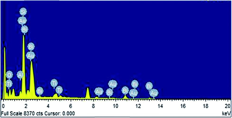 | ||
| Fig. 3 EDX measurements of Bi2O3 NSTs/Al nEFs. | ||
 | ||
| Fig. 4 FESEM image of (a) Bi2O3 micro-leaf structures (b and c) Bi2O3 NSTs (d) Bi2O3 NSTs/nano-Al nEFs, on an Au-coated Si substrate. | ||
The Fourier transform infrared spectrum (FT-IR) of the thin Bi2O3 NST film on the silicon substrate was obtained and is shown in Fig. 5. The band at wave number 1074.9 cm−1 is attributed to the stretching vibrations of the Si–O bond,20 indicating the presence of an SiO2 layer at the interface between deposited Bi2O3 NST thin film and the silicon substrate. The low vibration modes observed at wave numbers of 465.11 cm−1 and 610.69 cm−1 can be ascribed to the vibration of the Bi–O bond of the distorted BiO6 octahedral structural unit.21,22 The frequency band at wave number 818.83 cm−1 can be assigned to the stretching vibration of the Bi–O bond of the BiO3 species from the BiO6 octahedron.23
 | ||
| Fig. 5 FT-IR spectrum of Bi2O3 NSTs on a silicon substrate. | ||
The mechanism of formation of bismuth oxide structures on silicon chips has been described previously by Pathan et al.24 In the present case, we hypothesize an identical behavior. When the silicon chip is immersed into the first precursor solution, the bismuth hydroxyl ions become adhered to the chip due possibly to van der Waals forces or to electrostatic forces between the bismuth hydroxyl groups and the hydroxylated surface of SiO2. Note that the hydroxylation of the surface of SiO2 is due to the presence of water in the precursor. The adsorbed bismuth hydroxyl ions on the chip, when immersed in the second solution, react with hydrogen ions and form bismuth oxide, as per eqn (1) below.
| 2Bi(OH)4− + 2H+ → Bi2O3 + 5H2O | (1) |
Rinsing the chip with water removes the loosely bound or unreacted molecules. The growth of the bismuth oxide crystal proceeds layer by layer and the kinetics of this growth depend on the precursor concentration, deposition time and number of cycles. The gold nanoparticles on the surface of the Au-sputtered silicon wafer act as a catalyst by serving as a sink for interfacial charge transfer as they come into contact with the hydroxyl ions. Therefore, these nanoparticles then act as metalized centers to promote grain growth and nucleation for the favorable growth of bismuth oxide nanocrystals. It has been observed that, because of the very thin nature of the stack, the gold becomes deposited as a discontinuous layer, which gives us a basis for our hypothesis about nucleating gold sites, as detailed above. This interfacial interaction of the gold and bismuth oxide nanostructure enhances colloidal bond stability, as well as the stability at room temperature, and promotes favorable nanocrystal growth from these catalyst sites.
The TG-DSC studies of heat released during the thermite reactions of the 60, 100 and 140 nm aluminum-sputtered nEFs are shown in Fig. 6(a–c). Of these nEFs, the 140 nm Al-sputtered nEF developed the highest heat of reaction (ΔHr), at 710 J g−1 (peak temperature (Tp) of 589 °C), and its reaction was initiated at the lowest onset temperature (Ton), at 535 °C, compared to 60 nm-Al sputtered (Ton = 540 °C, ΔHr = 180 J g−1) and 100 nm-Al sputtered (Ton = 550 °C, ΔHr = 209 J g−1) nEFs. The residual masses of the nEFs formed with aluminum sputter-layers of 60, 100 and 140 nm were 108.4%, 103.2% and 100.2%, respectively, according to thermogravimetric studies of these samples. An interpretation of these thermogravimetric and DSC observations is that the aluminum sputter-layer of 140 nm nearly optimally satisfies the requirements of fuel to completely combust with Bi2O3 oxidizers. The endothermic peaks in all three nEFs, with aluminum sputter-layers of 60, 100 and 140 nm, were observed at onset temperatures of 645, 642 and 646 °C, respectively, with corresponding endothermic heat magnitudes of 17, 19 and 18 J g−1. The similar trends in the initiation and heat magnitudes of the endothermic peaks of all three nEFs can be attributed to the melting of aluminum. The thermogravimetric mass was observed to decrease as the temperature was increased up to about 460 °C, which may be attributed to consequences of thermal decomposition of bismuth trioxide and evaporation of any moisture adsorbed by bismuth trioxide. The thermogravimetric masses of all three nEFs were observed to start increasing from about 460 °C, i.e., they exhibited a residual mass above 100%, which can be attributed to the reaction of aluminum25 with residual oxygen impurity (<0.001%) in the nitrogen gas and the reaction of titanium26 with nitrogen in the temperature range of ∼460–650 °C. A similar25 trend of increasing mass from around 600 °C was observed during TG analysis of nanoenergetic Al/Co3O4 materials, due to reaction of aluminum with the small amount of oxygen present in the argon gas.
 | ||
| Fig. 6 TG-DSC measurements of nanoenergetic films of Bi2O3 NSTs/Al with an Al sputter-layer thicknesses of (a) 60 nm, (b) 100 nm and (c) 140 nm. | ||
Based on the above results of heat of reaction, nEFs with 140 nm sputter-layer of aluminum were selected for pressure–time characteristics measurements. The combustion was performed by blasting the scratched nEFs in a pressure cell experiment at a charge density of 0.2 g cm−3. The pressure–time characteristics measurements are shown in Fig. 7. Here, the peak pressure and its pressurization rate were measured to be 40.8 MPa and 4.08 MPa μs−1, respectively. This pressurization rate is markedly higher than that achieved by the combustion of the same charge density of nanothermite composites of aloe-vera-assisted CuO nanorods and aluminum.2 The higher gas-generating ability of this nEF contributed to enhancing the rate of increase of the peak pressure and hence the pressurization rate. A higher gas-generating ability and hence higher pressure build-up capability have been observed in other research studies as well.27,28
 | ||
| Fig. 7 Pressure–time characteristics measurement of Bi2O3/Al nEFs having an Al-sputter layer of 140 nm. | ||
A micropatterning trial of this process was carried out by producing a mask of PMMA with lines 200 microns wide obtained through laser micromachining of a PMMA substrate of 1 mm thickness. The micromachined PMMA sheet with the PDMS layer transferred by the stamp and stick bonding technique29 was used as a shadow mask throughout the deposition process, including the deposition of the Ti/Au stack, the aqueous chemical formation of the bismuth oxide NSTs, and the aluminum coating of the Bi2O3 NSTs. Fig 8(a) shows the photo images of titanium and gold sputtered PMMA-masked silicon substrates with the silicon substrate as the bottom layer and the PMMA mask as the top layer. The PMMA-masked silicon substrate showed no leakage during the fluorescent dye leak test (Fig. 8(b)), which clearly indicates that the PMMA mask was perfectly aligned and sealed the silicon substrate. Fig. 8(c) and (d) show the FESEM micrographs of the patterned nanoenergetic composites comprising Bi2O3 NSTs and a sputter coated aluminum layer. Fig. 8(e) and (f) show the FESEM image of 60°-inclined nEFs of Bi2O3/Al (aluminum sputter layer of 60 nm) micropatterned on a silicon substrate. From Fig. 8(c) and (e), it can be interpreted that the Bi2O3/Al nanoenergetic films formed with variable deposition thicknesses of Bi2O3, however, and from the high-magnification FESEM image Fig 8(f) (which is a magnified FESEM view of the circled section of Fig. 8(e)), the thickness of Bi2O3/Al was measured to be 320 ± 30 nm. From the FESEM observation, the Bi2O3 growth-thickness can be estimated to be of 260 ± 30 nm. The width of an individual composite pattern was found to be 203 ± 4 μm, whereas the average width of the mask holes was observed to be 205 ± 2 μm. This shows a reproducibility of the patterning to an accuracy of ±4 μm, which illustrates good resolution and localization according to the shadow guidance given by the mask. This indicates the relevance of this process towards micro-patterning of these composites, which can be utilized for micro-chip initiators, detonators, microthrusters and other pyrotechnic applications related to micro-chip manufacturing.
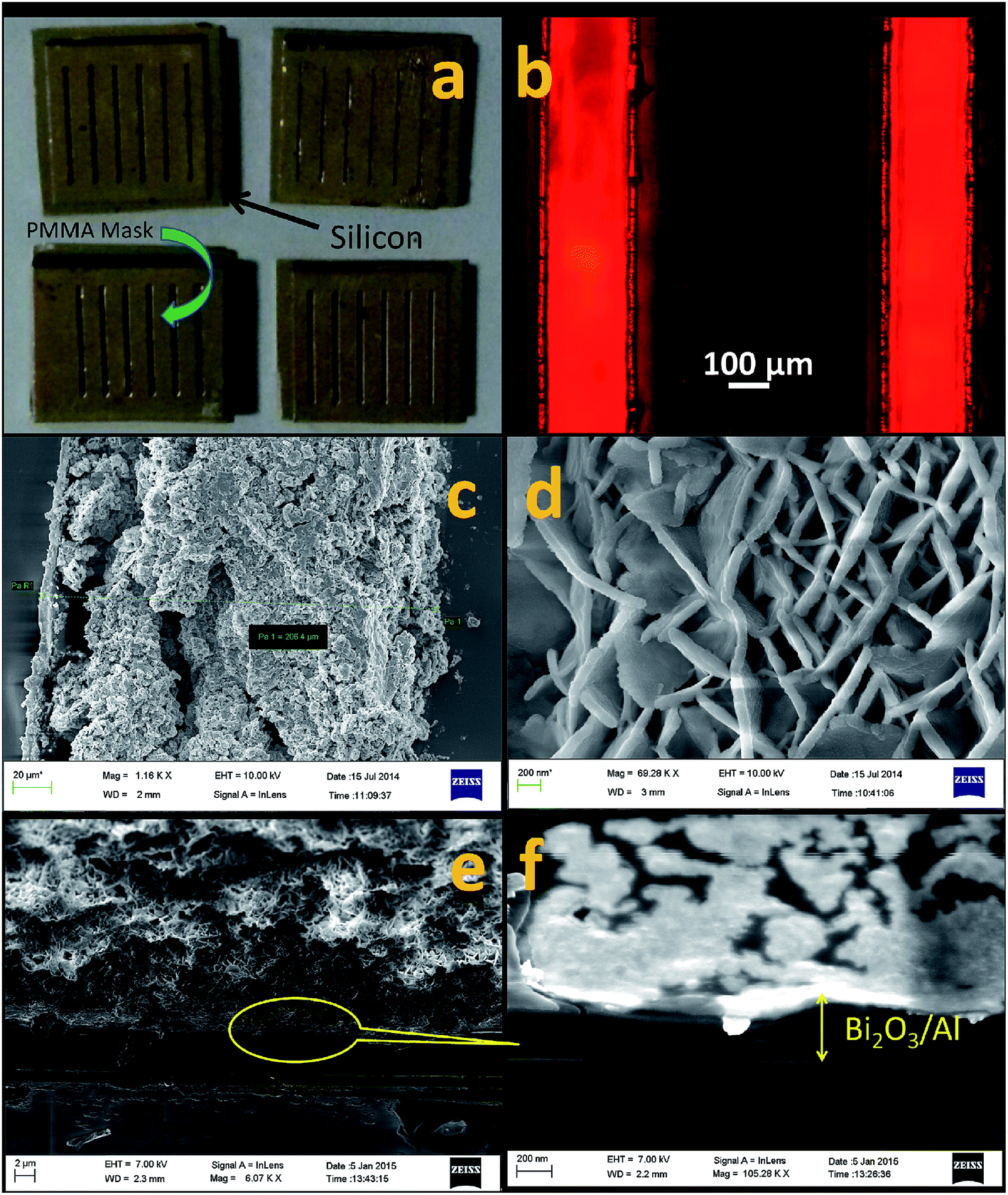 | ||
| Fig. 8 (a) Image of Ti and Au-sputtered PMMA-masked Si substrates (b) fluorescent dye leak test image of mask-channels (c and d) FESEM image of micropatterned Bi2O3/Al nEFs (e) FESEM image of inclined micropatterned Bi2O3/Al nEFs (f) High-magnification FESEM image of the circled section of the image in panel (e) showing a Bi2O3/Al deposition layer of 320 ± 30 nm for an Al sputter layer deposition of 60 nm. | ||
IV. Conclusions
Uniform and symmetric nano-square tablets of Bi2O3 were synthesized on a silicon substrate by catalytic assistance of gold nanoparticles. The gold nanoparticles are supposed to act as favorable active crystal sites for the stable colloidal growth of bismuth trioxide NSTs. In the absence of gold film on a silicon substrate, instead of Bi2O3 NSTs, micro-leaf structures formed. The FT-IR spectroscopy of the deposited thin film of Bi2O3 NSTs on silicon substrates showed the representative peaks of the SiO2 interfacial layer between the Bi2O3 NSTs and Si substrate, as well as the vibration bands of the Bi–O bond. Bi2O3/Al-based nanoenergetic films were produced by sputtering of aluminum of varied sputter-layer thicknesses of 60, 100 and 140 nm over chemically grown Bi2O3 NSTs. TG-DSC characterizations of Bi2O3/Al-based nEFs show that the exothermic reaction starts before the melting of aluminum, based on the solid-phase diffusion mechanism. The nEF formed by sputter deposition of 140 nm aluminum developed the greatest heat of reaction (710 J g−1) of the nEFs tested and initiated the reaction at an onset temperature of 535 °C, according to the TG-DSC measurement. This nanoenergetic film is able to generate a very high pressurization rate of 4.08 MPa μs−1 and a moderate peak pressure of 40.8 MPa in a combustion experiment in a constant-volume pressure-cell at a charge density of 0.2 g cm−3. Further micropatterning of these composites was carried out and it was observed that good patterning resolution could be obtained through this deposition process. This makes the process a promising candidate for manufacture of functional micro/nano devices in silicon for a variety of pyrotechnic applications.Acknowledgements
We sincerely thank the Science Engineering and Research Council, Department of Science and Technology (DST), Government of India for its financial support. The author would also like to acknowledge the Nanoscience and Soft Nanotechnology Centre, IIT Kanpur for providing good material characterization facilities. The authors also thank Netzsch Technologies India Pvt Ltd Chennai for its TG-DSC measurements.References
- V. E. Sanders, B. W. Asay, T. J. Foley, B. C. Tappan, A. N. Pacheco and S. F. Son, J. Propul. Power, 2007, 23, 707–714 CrossRef CAS.
- V. K. Patel and S. Bhattacharya, ACS Appl. Mater. Interfaces, 2013, 5, 13364–13374 CAS.
- C. Rossi, S. Orieux, B. Larangot, T. D. Conto and D. Esteve, Sens. Actuators, A, 2002, 99, 125–133 CrossRef CAS.
- S. Apperson, R. V. Shende, S. Subramanian, D. Tappmeyer, S. Gangopadhyay, Z. Chen, K. Gangopadhyay, P. Redner, S. Nicholich and D. Kapoor, Appl. Phys. Lett., 2007, 93, 243109 CrossRef.
- H. Pezous, C. Rossi, M. Sanchez, F. Mathieu, X. Dollat, S. Charlot, L. Salvagnac and V. Conedera, Sens. Actuators, A, 2010, 159, 157–162 CrossRef CAS.
- M. Korampally, S. J. Apperson, C. S. Staley, J. A. Castorena, R. Thiruvengadathan, K. Gangopadhyay, R. R. Mohan, A. Ghosh, L. Polo-Parada and S. Gangopadhyay, Sens. Actuators, B, 2012, 171–172, 1292–1296 CrossRef CAS.
- K. Zhang, C. Rossi, G. A. A. Rodriguez, C. Tenailleau and P. Alphonse, Appl. Phys. Lett., 2007, 91, 113117 CrossRef.
- M. Petrantoni, C. Rossi, V. Conedera, D. Bourrier, P. Alphonse and C. Tenailleau, J. Phys. Chem. Solids, 2010, 71, 80–83 CrossRef CAS.
- K. Zhang, C. Rossi, P. Alphonse, C. Tenailleau, S. Cayez and J.-Y. Chane-Ching, Appl. Phys. A, 2009, 94, 957–962 CrossRef CAS.
- Z. Qiao, D. Xu, F. Nie, G. Yang and K. Zhang, J. Appl. Phys., 2012, 112, 014310 CrossRef.
- C. S. Staley, C. J. Morris, R. Thiruvengadathan, S. J. Apperson, K. Gangopadhyay and S. Gangopadhyay, J. Micromech. Microeng., 2011, 21, 115015 CrossRef.
- D. H. Bao, T. W. Chiu, N. Wakiya, K. Shinozaki and N. Mizutani, J. Appl. Phys., 2003, 93, 497–503 CrossRef CAS.
- L. Leontie, J. Optoelectron. Adv. Mater., 2006, 8, 1221–1224 CAS.
- P. Shuk, H. D. Wiemhofer, U. Guth, W. Gopel and M. Greenblatt, Solid State Ionics, 1996, 89, 179–196 CrossRef CAS.
- N. Pugazhenthiran, P. Sathishkumar, S. Murugesan and S. Anandan, Chem. Eng. J., 2011, 168, 1227–1233 CrossRef CAS.
- T. P. Gujar, V. R. Shinde, C. D. Lokhande and S.-H. Han, Mater. Sci. Eng., B, 2006, 133, 177–180 CrossRef CAS.
- X.-P. Shen, S.-K. Wu, H. Zhao and Q. Liu, Phys. E, 2007, 39, 133–136 CrossRef CAS.
- M. Zhao, X. L. Chen, Y. J. Ma, J. K. Jian, L. Dai and Y. P. Xu, Appl. Phys. A, 2004, 78, 291–293 CrossRef CAS.
- P. V. Kamat and D. Meisel, Curr. Opin. Colloid Interface Sci., 2002, 7, 282–287 CrossRef CAS.
- P. G. Pai, S. S. Chao, Y. Takagi and G. Lucovsky, J. Vac. Sci. Technol., 1986, A4, 689–694 CrossRef.
- P. S. Rao, C. Rajyasree, A. R. Babu, P. M. V. Teja and D. K. Rao, J. Non-Cryst. Solids, 2011, 357, 3585–3591 CrossRef CAS.
- M. Bosca, L. Pop, G. Borodi, P. Pascuta and E. Culea, J. Alloys Compd., 2009, 479, 579–582 CrossRef CAS.
- F. He, J. Wang and D. Deng, J. Alloys Compd., 2011, 509, 6332–6336 CrossRef CAS.
- H. M. Pathan and C. D. Lokhande, Bull. Mater. Sci., 2004, 27, 85–111 CrossRef CAS.
- D. Xu, Y. Yang, H. Cheng, Y. Y. Li and K. Zhang, Combust. Flame, 2012, 159, 2202–2209 CrossRef CAS.
- J. Nulmain, U. S. Pat., 5236868, 1993.
- J. A. Puszynski, C. J. Bulian and J. J. Swiatkiewicz, J. Propul. Power, 2007, 23, 698–706 CrossRef CAS.
- K. S. Martirosyan, J. Mater. Chem., 2011, 21, 9400–9405 RSC.
- S. Satyanarayana, R. N. Karnik and A. Majumdar, J. Microelectromech. Syst., 2005, 14, 392–399 CrossRef.
| This journal is © The Royal Society of Chemistry 2015 |