An anode buffer layer with size-controlled Ag nanoparticles for polymer solar cells with improved efficiencies

Dhanavel Ganeshanab, Shan-Ci Chena, Zhigang Yinab and Qingdong Zheng*a
aState Key Laboratory of Structural Chemistry, Fujian Institute of Research on the Structure of Matter, Chinese Academy of Sciences, 155 Yangqiao West Road, Fuzhou, Fujian 350002, P. R. China. E-mail: qingdongzheng@fjirsm.ac.cn
bUniversity of Chinese Academy of Sciences, Beijing 100049, P. R. China

Received 27th November 2014 , Accepted 26th January 2015

First published on 26th January 2015


Abstract

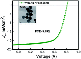
We systematically studied the plasmonic effects in polymer solar cells (PSCs) by using an anode buffer layer, in which size-controlled silver nanoparticles (NPs) (diameter: 4, 28, 55, and 75 nm, respectively) are incorporated into poly(3,4-ethylenedioxythiophene):poly(styrenesulfonate) (PEDOT:PSS). The optical properties of the buffer layer as well as the device performance of the resulting devices were investigated. We found that Ag NPs with an average diameter of 55 nm showed good behavior on enhancing light absorption due to the plasmonic scattering effect. Subsequently, the power conversion efficiency (PCE) of the PSC with Ag NPs (55 nm) improves to as high as 9.45% in comparison with a value of 7.90% for the control device without Ag NPs. In addition, the open circuit voltage, photocurrent and fill factor are simultaneously increased. The external quantum efficiency and light absorption are significantly enhanced in the range of ∼400–550 nm as compared to the control device. These results demonstrate that embedding Ag NPs into PSCs offers an effective strategy to improve the performance of optoelectronic devices.


1. Introduction

Organic bulk-heterojunction (BHJ) polymer solar cells (PSCs) with an active layer composed of a conjugated polymer (p-type) and a fullerene derivative (n-type) have several advantages such as light weight, mechanical flexibility, large-area fabrication and low-cost production of electronic devices.1–3 Recently, significant advances have been made in low-bandgap polymer materials with deep highest occupied molecular orbital (HOMO) energy level to harvest a wide solar spectrum and to achieve a high power conversion efficiency (PCE) of PSCs.4 As a result, the highest PCE of 10.01% from a single-junction BHJ solar cell has been achieved so far.5 However, further improvement of PCEs is still necessary for commercialization. Many attempts have thus been made in recent years to improve the PSC performance, such as the introduction of electrode buffer layers, optimization of film morphology, and development of new device architectures.6 Moreover, researchers also tried to synthesize various types of conjugated polymer materials that have broad absorption spectra, high carrier mobilities and appropriate energy levels to achieve high open circuit voltages (Voc) of PSCs. All of these efforts led to organic BHJ solar cells with over 10% PCEs for single junction devices and possibly reaching 15% in tandem devices.5,7,8

Although the PCEs of BHJ solar cells have been sharply boosted in the past decade, these efficiencies are still lower than those of silicon-based solar cells due to insufficient light absorption, low carrier mobilities and short exciton diffusion lengths within thin films.9 Various approaches were taken to enhance the light absorption without increasing the thickness of the BHJ layer, so as to improve the short circuit current.7 Recently, researchers introduced noble metallic nanoparticles (NPs) such as gold (Au), silver (Ag), copper (Cu) and platinum (Pt) into organic photovoltaic (OPV) devices for an enhanced light harvesting by utilizing the localized surface plasmonic resonances (LSPR) effect.6,10–17 Several research groups already have reported PCE enhancements by incorporating metallic NPs into OPV devices.11,13–16,18–25 In particular, Au and Ag NPs are attracting increasing attention due to their strong LSPR properties. Up to now, plasmonic enhancement is considered to be one of the best approaches due to its simple process, effectiveness,13 conductivity,9 surface morphology,26 and tunable particle size, shape, and composition.

Incorporating metal NPs into the poly(3,4-ethylenedioxythiophene):poly(styrenesulfonate) (PEDOT:PSS) buffer layer is a straightforward method to take advantages of plasmonic photovoltaic effects. In this case, LSPR can be used for enhancing light absorption.27 Ag and Au NPs were commonly used as a plasmonic material due to their efficient light harvesting in a broad range of wavelength and better stability than any other metal NPs. Many previous reports have investigated how plasmonic PSCs can have enhanced light absorption and high external quantum efficiencies (EQEs).4,7–9,16,24,26,28–31 However, systematic studies on plasmonic PSCs with size-controlled NPs are relatively rare. Here, we used Ag NPs because they have several advantages: (1) excellent light absorption in the solar spectrum; (2) enhancement in exciton generation rate and dissociation efficiency;7 (3) enhanced charge carrier density and the exciton lifetime;29 (4) easy synthesis of the quasi-spherical NPs; and (5) suitability for large-area, roll-to-roll mass production techniques. Therefore, plasmonic photovoltaic effects have been frequently used for the design of various optoelectronic devices.

In this paper, we fabricated PSCs with a conventional device structure of ITO/PEDOT:PSS-Ag NPs/PTB7-Th:PC71BM/PFN/Al, where PEDOT:PSS-Ag NPs is a hole-collecting buffer layer based on PEDOT:PSS doped with various sizes of quasi-spherical Ag NPs (diameter: 4, 28, 55, and 75 nm, respectively), PTB7-Th is a low-bandgap polymer material, poly[4,8-bis(5-(2-ethylhexyl)thiophen-2-yl)benzo[1,2-b:4,5-b′]dithiophene-co-3-fluorothieno[3,4-b]thiophene-2-carboxylate], PC71BM is a fullerene derivative, [6,6]-phenyl C71-butyric acid methyl ester, and PFN is an alcohol-soluble polymer, poly[(9,9-bis(3′-(N,N-dimethylamino)propyl)-2,7-fluorene)-alt-2,7-(9,9-dioctylfluorene)]. Ag NPs with an average diameter of 55 nm showed better scattering efficiency as compared to other sized Ag NPs and the resulting plasmonic PSCs exhibited a high PCE of 9.45%. Furthermore, we systematically studied the size effect of Ag NPs on the PSC performance, and found that the Ag NPs with 55 nm are the most suitable for enhancing the PSC device efficiency by the increased hole collection and light absorption of the active layer by the LSPR effect as well as the optimized morphology in the interface.

2. Experimental

2.1. Materials

PTB7-Th was prepared according to the literature procedures3 and PC71BM was purchased from American Dye Source Inc (Canada), chlorobenzene (CB)/1,8-diiodooctane from Sigma-Aldrich Inc, and PFN was purchased from Derthon Optoelectronic Materials Science & Technology Co. Ltd (China), respectively, and used as received. Silver nitrate (99.8%), sodium borohydride (98%), and trisodium citrate dihydrate (99%) were all purchased commercially and used without further purification.

2.2. Synthesis of Ag NPs

Ag NPs with average diameters of 4, 28, 55, and 75 nm were synthesized with the method described in the literature.32 The synthetic details are as follows.
2.2.1. 4 nm Ag NPs. For the synthesis of 4 nm Ag NPs, 20 mL of 1% (w/w) citrate solution and 75 mL of water were added in a round bottom flask and the mixture was heated to 70 °C for 15 min. After that, 1.7 mL of 1% (w/w) AgNO3 solution was introduced to the mixture, followed by a quick addition of 2 mL of 0.1% (w/w) freshly prepared NaBH4 solution. The reaction solution was kept at 70 °C under vigorous stirring for 1 h and cooled to room temperature. Water was added to bring the volume of the dispersion to 100 mL. The resulting Ag NPs have a size of 4 nm, and were also used as starter seeds for preparing other Ag NPs with larger sizes.
2.2.2. 28 nm Ag NPs. For the synthesis of 28 nm Ag NPs, the first step was similar to the 4 nm Ag NPs synthesis procedure. 2 mL of 1% citrate solution was mixed with 75 mL of water and brought to boiling by a heating mantle for 15 min. Next, 10.0 mL of the starter seed solution was added while vigorous stirring, followed by the addition of 1.7 mL of 1% AgNO3 solution. The stirring continued for 1 h at reflux. The next step was then performed by adding 2 mL of 1% citrate solution to the reaction solution together with 1.7 mL of 1% AgNO3 solution. Reflux with vigorous stirring continued for another one hour. The same operation was then repeated. After that, the reaction solution was cooled to room temperature. Water was added to bring the volume to 100 mL.
2.2.3. 55 nm Ag NPs. For the synthesis of 55 nm Ag NPs, the resulting 28 nm Ag NPs were used as seeds. 2 mL of 1% citrate solution was mixed with 80 mL of water and heated to 80 °C by a water-bath for 15 min. Next, 10.0 mL of the seed solution was added while vigorous stirring, followed by the addition of 1% AgNO3 solution (1.7 mL). The reaction solution was kept at 80 °C under vigorous stirring for 2 h and cooled to room temperature. Water was added to bring the volume to 100 mL.
2.2.4. 75 nm Ag NPs. For the synthesis of 75 nm Ag NPs, the 55 nm Ag NPs were used as seeds. 30 mL of the seed solution was mixed with 60 mL of water and heated to 80 °C by a water-bath for 15 min. Next, 2 mL of 1% citrate solution was added while vigorous stirring, followed by the addition of 1% AgNO3 solution (1.7 mL). The reaction solution was kept at 80 °C under vigorous stirring for 2 h and cooled to room temperature.

2.3. Device fabrication

The ITO-coated glass substrate with a sheet resistance of ∼15 Ω sq.−1 was used for the device fabrication. The ITO-glass substrates were first cleaned with detergent, ultrasonication in water, acetone and isopropanol for 30 min each, and subsequently dried at 130 °C overnight in an oven, followed by a UV ozone treatment for 15 min. Various sized Ag NPs solutions were sonicated for 10 min at room temperature (RT) before they were mixed with PEDOT[thin space (1/6-em)]:[thin space (1/6-em)]PSS (Al4083, Baytron) at a weight ratio of 5[thin space (1/6-em)]:[thin space (1/6-em)]1 by stirring for 10 min at RT. Then, a PEDOT:PSS layer with or without various sized Ag NPs was spun onto the substrates at 3000 rpm for 60 s and annealed at 130 °C for 30 min in air. Thereafter, PTB7-Th[thin space (1/6-em)]:[thin space (1/6-em)]PC71BM (1[thin space (1/6-em)]:[thin space (1/6-em)]1.5 w/w) was spun at 1600 rpm for 60 s on top of the anode buffer layer from CB–1,8-diiodooctane (v/v, 97[thin space (1/6-em)]:[thin space (1/6-em)]3) solution in a glove box. Later, the PFN solution (0.3 mg mL−1 in methanol) was spin-coated on top of the obtained active layer at a spin speed of 1500 rpm for 30 s to form a thin interlayer.33 Then the devices were kept at room temperature overnight. Finally, an Al cathode (95 nm) was deposited on top of the interlayer through shadow masks by thermal evaporation at a chamber pressure of (∼1 × 10⁻⁴ Pa). The active area of all conventional devices was fixed at 0.04 cm2.

2.4. Particle and device characterization

The size of the Ag NPs was characterized by a transmission electron microscopy (TEM). High-resolution TEM (HR-TEM) images of the NPs were obtained a FEI Tecnai G2 F-20 S-TWIN with an accelerating voltage of 200 kV. HR-TEM was carried out to confirm the interplanar crystal spacing of the Ag NPs. A selected area electron diffraction (SAED) was also performed to investigate the crystallinity of single NP. The scanning electron microscopy (SEM) images were obtained with a JSM-6700F (JEOL) operated at 80 kV. The current density–voltage (JV) characteristics of PSCs were taken under AM 1.5G irradiation at 100 mW cm−2 from an Oriel Sol3A simulator (Newport) with a NREL-certified silicon reference cell. The JV curves were obtained by a Keithley 2440 source measurement unit. The EQE spectra were measured on a Newport EQE measuring system. EQE measurements were conducted under chopped monochromatic light from an optical fiber in an under filled geometry without bias illumination. The UV-vis absorption and transmission measurements were carried out at RT with a Lambda35 spectro-photometer. Atomic force microscopy (AFM) images were obtained with a Veeco Multimode NS3A-02 NanoScope III atomic force microscope.

3. Results and discussion

3.1. Characterization of Ag NPs

Ag NPs were prepared by the reduction of silver nitrate (AgNO3) with sodium borohydride (NaBH4) at an elevated temperature in the presence of the concentrated trisodium citrate (experiment section for more details). The as-prepared Ag NPs were of a quasi-spherical shape and had relatively uniform diameters. For clarity, magnified TEM images of different sizes of Ag NPs are shown in Fig. 1a. It is observed that the average sizes of these Ag NPs are approximately 4, 28, 55 and 75 nm, respectively. For Ag NPs of varying sizes, most NPs were found to be spherical and monodispersed. The distinct boundary between Ag NPs is clearly visible due to the well controlled size and shape of these Ag NPs. As a further investigation, uniform films of these NPs were coated on silicon substrates via drop-casting, as confirmed by SEM images, demonstrating the well dispersing behavior of these Ag NPs (in Fig. S2). The results showed that Ag NPs can be prepared in sizes up to 75 nm through the stepwise growth process, and there is no reason against obtaining Ag NPs with even larger sizes.32 However, NPs with an average diameter of 55 nm are found to be the most suitable for high performance PSCs. In this work, we verified the size of 55 nm Ag NPs by the TEM measurement. Fig. S3a and b show the typical TEM and HR-TEM images for the as-transformed product, respectively, confirming the interplanar crystal spacing of the Ag NPs. The SAED patterns demonstrated the concentric diffraction rings as bright spots corresponding to the presence of (111), (200), and (220) planes of the face-centered cubic (fcc) Ag NPs.34 The crystalline nature of a single particle was further investigated by means of HR-TEM with the d-spacing value. For Ag NPs with the average size of 55 nm, the observed d-spacings corresponding with the (111) and (200) planes were 0.226 and 0.210 nm, respectively (Fig. S3c), which were obtained by focusing an electronic beam on the zone axis of an individual NP. For Ag NPs with a higher average particle size (>50 nm), HR-TEM images showed the presence of multiple-twinned crystalline planes. In Fig. S3b, there is a five-fold multiple twinned decahendron crystal, which is favored for the fcc growth of Ag.35 It can clearly be seen that the Ag NPs were successfully synthesized with a well-defined quasi-spherical morphology. The Ag NPs are imbedded in the PEDOT:PSS anode layer with slight aggregation (Fig. S4). However, the size and shape of the Ag NPs in PEDOT:PSS are basically the same as those of pure Ag nanoparticles.
image file: c4ra15343j-f1.tif
Fig. 1 (a) TEM images of various sized Ag NPs. The average NPs sizes are about 4, 28, 55 and 75 nm. (b) Corresponding UV-vis absorption spectra of these Ag NPs solution dispersed in water, all spectra are normalized at their absorption maxima, which are 395, 422, 446, and 485 nm, respectively.

The UV-vis absorption spectra of these Ag NPs solution dispersed in water are shown in Fig. 1b. Corresponding to the excitation of LSPR, the absorption peaks for these Ag NPs are at 395, 422, 446, and 485 nm, respectively, which all locate at the absorption of most BHJ films. As predicted, Ag NPs exhibited bathochromically shifted absorption maxima with an increase in the Ag NPs size. The broadened absorption band was however inevitable since a broader size distribution was obtained for larger Ag NPs (>50 nm).34 Nonetheless, the broadened absorption will help to improve the light harvesting ability of PSCs.

Fig. 2a illustrates that the scattering/absorption spectra of bare ITO-glass, neat PEDOT:PSS and PEDOT:PSS with various sized Ag NPs. It can be observed that there is no big difference between neat PEDOT:PSS and PEDOT:PSS with Ag NPs films indicating that the Ag NPs with various sizes are all well dispersed in the PEDOT:PSS film without any serious aggregation. We also investigated the transmission of PEDOT:PSS with/without Ag NPs and observed no discernible difference (Fig. 2b). All five ITO/PEDOT:PSS with and without Ag NPs substrates show good optical transparency of over 80% average transmittance with little deviation from the bare ITO-glass. Furthermore, the film transmittance of PEDOT:PSS with Ag NPs is influenced by the size of Ag NPs solutions because there is a small shift towards long wavelength as compared to the neat PEDOT:PSS film. It can be seen from Fig. 2b that the transmission of the ITO/PEDOT:PSS films with various sized Ag NPs in the range of ∼550–800 nm is similar, no matter whether the PEDOT:PSS layer was embedded with Ag NPs or not. In the range of ∼400–550 nm, the transmission of the ITO/PEDOT:PSS films with various sized Ag NPs are slightly lower than that of the ITO glass without Ag NPs.


image file: c4ra15343j-f2.tif
Fig. 2 UV-vis scattering/absorption (a) and optical transmission spectra (b) of PEDOT:PSS films with/without Ag NPs.

3.2. Device structure of PSCs using plasmonic Ag NPs

The device structure of plasmonic PSCs is illustrated in Fig. 3a. The Ag NPs with four different sizes were incorporated into the PEDOT:PSS layer, respectively, to induce the plasmonic scattering effect. NPs solution was mixed with the PEDOT[thin space (1/6-em)]:[thin space (1/6-em)]PSS solution in a volume ratio of 5[thin space (1/6-em)]:[thin space (1/6-em)]1 and spun onto the substrate. Fig. 3b illustrates the molecular structures of PTB7-Th as an electron donor and PC71BM as an electron acceptor. The control device structure was glass/ITO/PEDOT:PSS/PTB7-Th:PC71BM/PFN/Al. It has been reported that the result of the control devices based on PTB7-Th:PC71BM showed PCEs of approximately 7.42%[thin space (1/6-em)]36 and 7.64%,3 respectively. Therefore, to further increase the PCE before the addition of Ag NPs, we optimized the control device by using PFN interlayer between the photoactive layer and the metal cathode. The control devices exhibited a PCE of approximately 7.90%.
image file: c4ra15343j-f3.tif
Fig. 3 (a) The device structure of plasmonic PSCs used in this work. (b) Molecular structures of the active layer materials.

In fact, plasmonic PSCs by using Ag NPs doped-PEDOT:PSS with different active layers have been reported by several groups, and PCEs of approximately 8.6%,29 8.01%,7 and 7.29%[thin space (1/6-em)]4a were reported. In this work, a novel combination of the device structure and the active layer is chosen to further improve the efficiency of plasmonic PSCs. Ag NPs with different sizes are incorporated into the PEDOT:PSS buffer layer, the PTB7-Th:PC71BM active layer was the spin-coated on the PEDOT:PSS followed by spin-coating the PFN as a cathode buffer layer. Consequently, we achieved a high PCE of 9.45% for the single junction BHJ solar cells, leading to approximately 20% PCE improvement as compared to the control devices. The effects of Ag NPs have been investigated from a device fabrication perspective. The effects of Ag NPs on the optical properties of the buffer layer have been studied. Our results show that both the enhanced light harvesting ability and the improved charge collection efficiency at donor/acceptor junctions,7,26 contribute to enhance the device performance.

3.3. Plasmonic PSCs with different sizes of Ag NPs

Plasmonic PSCs with the device structure of ITO/Ag NPs doped-PEDOT:PSS/PTB7-Th:PC71BM/PFN/Al were fabricated and measured. Corresponding JV characteristics of PSCs incorporated with/without Ag NPs are shown in Fig. 4a. Table 1 shows the size effects of the embedded Ag NPs on the best performance PSCs. For reliability of the results, at least 100 devices were fabricated under each condition. After incorporating Ag NPs with the average diameter of 4 nm into PEDOT:PSS layer, the Voc remained nearly the same, the short-circuit current density (Jsc) increased from 16.81 to 17.47 mA cm−2, and the fill factor (FF) increased from 58.77 to 60.48%. As a result, the PCE enhanced from 7.90 to 8.48%. Incorporating 28 nm Ag NPs into PEDOT:PSS layer, the resulting PSCs show a slightly reduced Voc, an improved Jsc of 17.65 mA cm−2, an increased FF of 61.26%, and an enhanced PCE of 8.64%. Interestingly, devices with 55 nm Ag NPs showed much better device performance with the Jsc further improved to 17.82 mA cm−2, FF enhanced to 65.37% and Voc slightly increased, resulting in the highest PCE of 9.45%. Further increasing the size of Ag NPs, the PCE value drops to 9.06% (75 nm Ag NPs). Although the devices with 75 nm Ag NPs showed an enhanced Jsc value, the FF and the Voc were both reduced as shown in Fig. 5, which contributed to a decrease in PCE. The average photovoltaic parameters of plasmonic PSCs with four different sizes of Ag NPs are summarized in Table 1. Typically, devices with 55 nm Ag NPs showed a mean Voc of 0.811 ± 0.001 V, a Jsc of 17.94 ± 0.12 mA cm−2, and an FF of 64.38 ± 0.99%. The average PCEs for plasmonic PSCs with various sized Ag NPs (4, 28, 55, and 75 nm) are 8.17 ± 0.31%, 8.40 ± 0.24%, 9.36 ± 0.09%, and 8.28 ± 0.78%, respectively. The small standard deviations indicate good reliability and reproducibility of the PSCs in this work.
image file: c4ra15343j-f4.tif
Fig. 4 (a) Current–voltage characteristics, recorded under AM 1.5G illumination at 100 mW cm−2, of devices incorporating PEDOT:PSS doped with various sizes of Ag NPs. (b) EQE spectra and corresponding integrated Jsc curves of PTB7-Th/PC71BM without Ag NPs and with Ag NPs.
Table 1 Photovoltaic performance of plasmonic PSCs incorporating size-controlled Ag NPs in the PEDOT:PSS layer. The table shows the average solar cell performance for devices based on each size of Ag NPsa
Ag NPs (nm) Voc (V) Jsc (mA cm−2) FF (%) PCE (%) Rs (Ω cm2) Rsh (KΩ cm2)
a In the brackets illustrates the best solar cell performance. The Rs and Rsh were calculated according to the inverse of the slopes of the corresponding JV curves under illumination at V = 0 and J = 0, respectively.
Control device 0.797 ± 0.003 (0.800) 16.90 ± 0.09 (16.81) 56.57 ± 2.20 (58.77) 7.62 ± 0.28 (7.90) (10.62) (0.44)
Ag NPs (4 nm) 0.796 ± 0.007 (0.803) 17.20 ± 0.27 (17.47) 59.70 ± 0.78 (60.48) 8.17 ± 0.31 (8.48) (9.87) (0.54)
Ag NPs (28 nm) 0.799 ± 0.000 (0.799) 17.66 ± 0.01 (17.65) 59.58 ± 1.68 (61.26) 8.40 ± 0.24 (8.64) (9.23) (0.55)
Ag NPs (55 nm) 0.811 ± 0.001 (0.812) 17.94 ± 0.12 (17.82) 64.38 ± 0.99 (65.37) 9.36 ± 0.09 (9.45) (7.62) (0.70)
Ag NPs (75 nm) 0.797 ± 0.002 (0.799) 17.96 ± 0.11 (18.07) 57.89 ± 4.92 (62.81) 8.28 ± 0.78 (9.06) (8.64) (0.49)


image file: c4ra15343j-f5.tif
Fig. 5 The maximum enhancement for PSCs based on Ag NPs with various sizes under the optimized conditions.

Besides, the series resistance (Rs) and shunt resistance (Rsh) of the devices, obtained from the inverse slopes of the dark JV curves under illumination at V = 0 and J = 0, respectively, are also listed in Table 1. The series resistance (Rs) of the devices with Ag NPs decreased compared with the control devices. Especially, the Rs of PSCs with 55 nm Ag NPs reduced from 10.62 Ω cm2 (without Ag NPs) to 7.62 Ω cm2 (with 55 nm Ag NPs), and Rsh increased from 0.44 to 0.70 KΩ cm2. Consequently, the FF increased from 58.77% (without Ag NPs) to 65.37% (with 55 nm Ag NPs). The relatively small Rs, and large Rsh, are found for the devices with 55 nm Ag NPs doped in the anode buffer layer. Further increasing the size of Ag NPs from 55 nm to 75 nm, larger Rs and smaller Rsh, are found for the resulting PSCs. These parameter changes are also reflected by a decrease of FF from 65.37% (55 nm) to 62.81% (75 nm). To understand the size dependency of the PCE enhancement, we investigate the EQE and absorption of the plasmonic PSCs based on different sizes of Ag NPs.

3.4. Light harvesting and external quantum efficiencies

External quantum efficiency (EQE) measurements of PSCs are conducted to better elucidate the improved Jsc induced by the plasmonic NPs. Fig. 4b depicts the corresponding EQE spectra. Both devices based on 55 nm and 75 nm NPs have higher EQE values than those of the devices with small NPs or the control devices, which is in agreement with their increased PCEs as shown in Table 1. Thus, the increased EQEs for the PSCs with greater than 50 nm Ag NPs in the PEDOT:PSS layer can be attributed to the salient plasmonic effect of Ag NPs. The integrated Jsc values from the EQE spectra for five best performance devices are 16.78, 16.82, 16.98, 17.48, and 17.94 mA cm−2, respectively. The differences between integrated Jsc and measured Jsc are within 4%, indicating the good accuracy of the PSC efficiency measurement (Table S1).

To investigate the origin of the Jsc enhancement, we also performed UV-vis absorption measurements of BHJ films with/without Ag NPs. The absorption spectrum is shown in Fig. 6a. We found that the active layer (PTB7-Th:PC71BM) absorption in the region of 450 to 530 nm is enhanced after the incorporation of 4 nm Ag NPs or 28 nm Ag NPs. Incorporation of 55 nm Ag NPs not only leads to a further absorption enhancement in the region of 450 to 530 nm, but also leads to an increased absorption band from 450 to 720 nm. When the size of Ag NPs increases from 55 nm to 75 nm, the absorption peaks increase slightly. The maximum absorption enhancement percentages for PSCs with 4, 28, 55, and 75 nm Ag NPs are 8, 18, 33, and 38%, respectively. On the basis of EQE and UV-vis absorption results, it is clear that devices with 75 nm Ag NPs have enhanced absorption compared with those with 55 nm NPs or the control devices. However, in this work it is found that the devices with 55 nm Ag NPs exhibit around 20% enhancement in PCE due to the notable enhanced Voc, Jsc, and improved FF as shown in Fig. 5. Although the devices with 75 nm Ag NPs have the highest Jsc, the corresponding FF decreases, leading to a moderate PCE of 9.06%.


image file: c4ra15343j-f6.tif
Fig. 6 (a) UV-vis absorption spectra of PTB7-Th/PC71BM with/without Ag NPs. (b) Corresponding absorption enhancements of PSCs by incorporating various size-controlled Ag NPs.

3.5. AFM results

Fig. 7 illustrates the AFM images of PEDOT:PSS with/without Ag NPs. The root-mean-squared (RMS) roughness of PEDOT:PSS layer on ITO glass is measured to be 0.948 nm, while PEDOT:PSS mixed with Ag NPs showing the RMS roughness slightly larger than the PEDOT:PSS layer. Thus we could anticipate that all the Ag NPs are planted within the PEDOT:PSS layer so that the RMS roughness changed from 0.948 to 0.968, 1.006, 1.027, and 1.246 nm, in that order. It is reasonable that the roughness will increase as the size of Ag NPs increases. It has been reported that the increase of anode surface roughness can lead to the enlarged interface area between the anode and the active layer, allowing a relatively short route for holes to reach the anode and enhancing the hole collection efficiency as well.37,38 Accordingly, in this work, it is expected that the incorporation of larger Ag NPs will induce an increase of interfacial area between PEDOT:PSS and PTB7-Th:PC71BM, leading to an improvement in hole collection efficiency at the anode, thus increasing the Jsc of the resulting devices. It is the reason why the devices with 4 and 28 nm Ag NPs can achieve slightly improved Jsc (17.47 and 17.65 mA cm−2) despite there are no significant absorption enhancement in these devices. For the devices with 55 and 75 nm Ag NPs, increased Jsc of 17.82 mA cm−2 (55 nm) and 18.07 mA cm−2 (75 nm) are obtained compared to the Jsc of 16.81 mA cm−2 for the device without Ag NPs. This Jsc enhancement can be attributed to both the increased hole collection and the light absorption of the active layer by the LSPR effect. The photocurrent enhancement may also come from the morphology changes of the PEDOT:PSS due to the use of large size metal NPs.
image file: c4ra15343j-f7.tif
Fig. 7 Tapping mode AFM (1 × 1 μm) topographical images of ITO/PEDOT:PSS with/without Ag NPs: (a) PEDOT without Ag NPs; (b) PEDOT with 4 nm Ag NPs; (c) PEDOT with 28 nm Ag NPs; (d) PEDOT with 55 nm Ag NPs; and (e) PEDOT with 75 nm Ag NPs. All the films were coated on ITO glass. The corresponding mean roughnesses (RMS) of these films are 0.948, 0.968, 1.006, 1.027, and 1.246 nm, respectively.

Besides, the large size Ag NPs increase the interfacial area between PEDOT:PSS and PTB7-Th:PC71BM, and they also increase the plasmonic effect of Ag NPs.39 It is a positive effect to improve the FF of the resulting devices. Meanwhile, the series resistance of the devices with 4 or 28 nm Ag NPs is smaller than the control device, which is favorable to the increased FF; while the series resistance of the devices with 55 or 75 nm Ag NPs is much smaller than the control device, resulting in a much higher FF. Therefore, the combination of these effects leads to the trend in FF variation as shown in Table 1: the magnitudes of FF in the resulting devices increase from 59.90% (control device) to 60.48% (4 nm), 61.26% (28 nm), 65.37% (55 nm) and then decrease to 62.81% (75 nm) as the size of Ag NPs increases. The decreased FF for the devices based on 75 nm Ag NPs can be attributed to the increased carrier traps induced by the rougher PEDOT:PSS surface.

3.6. Optimized photovoltaic performance

In order to clarify the size effect of Ag NPs in PSC devices, we investigated the optical properties of active layers and the device parameters for the resulting PSCs based on NPs with various sizes. We first measured the absorption spectra of PTB7-Th:PC71BM active layers on top of ITO/PEDOT:PSS with different sizes of Ag NPs, as shown in Fig. 6a. During the measurement of light absorption, interestingly, the devices with smaller Ag NPs (4 and 28 nm) have no significant difference in light absorption compared with the control device without Ag NPs, while there are obvious absorption enhancements in the devices with larger Ag NPs (55 and 75 nm). It has been reported that when Ag NPs are incorporated into the PEDOT:PSS layer, the strong LSPR near-field around Ag NPs is mainly due to their superior scattering efficiency compared to other metal NPs.7,29

Even though there are no significant absorption changes of the active layer in the devices with smaller NPs (below 30 nm), EQE of these devices enhances considerably. For the devices with larger NPs (above 50 nm), EQEs of these devices in the range of ∼400–550 nm improved significantly as shown in the Fig. 4b. An efficiency enhancement of 20% was obtained, mainly due to LSPR induced by the metallic NPs, which led to a noticeable enhancement of Jsc. Therefore, it can be concluded that the thickness of Ag NPs greater than 50 nm showed high scattering efficiency and good electric behavior as compared to the control devices and small size Ag NPs. We optimized the performance of the resulting devices, the devices with 55 nm Ag NPs showed the highest efficiency as compared to any other devices in this paper. As a result, a high PCE of 9.45% was achieved. In addition, the open circuit voltages, photocurrents, and fill factors of the PSC devices were enhanced significantly by the incorporation of the 55 nm Ag NPs. The JV curves and EQE characteristics of the devices with 55 nm Ag NPs and without Ag NPs are illustrated in Fig. S5. As shown in Fig. S5b, the photocurrent responses in the range of ∼400–550 nm show that the average EQEs are 72% and 59% for the devices with 55 nm Ag NPs and without Ag NPs, respectively. Note that the theoretical Jsc values obtained by integrating the EQE data under the AM 1.5G solar spectrum are 17.48 mA cm−2 and 16.78 mA cm−2 (Table S1), respectively, which are in good agreement with values obtained from the JV characteristics (17.82 and 16.81 mA cm−2 in Fig. S5a). The difference between intergraded Jsc and measured Jsc is within 2%.

Moreover, the PEDOT:PSS film with 55 nm Ag NPs provide a similar grain size and thus can be used as an efficient anode buffer layer in conventional PSCs for forming good electric contacts with the BHJ layer and thus improving charge collection efficiency. On the whole, it can be concluded that the improved hole collection at the interface between PEDOT:PSS and PTB7-Th:PC71BM enhances device performances, while a slight reduction in PEDOT:PSS resistance by the incorporation of Ag NPs may also provide a minor contribution to the improved device performance.

4. Conclusions

In this study, we have demonstrated highly efficient plasmonic PSCs by simply incorporating different sizes of Ag NPs (diameter: 4, 28, 55, and 75 nm) into the PEDOT:PSS buffer layer. The optical and electrical properties of the PSCs with Ag NPs have been systematically investigated. On one hand, the smaller sized Ag NPs (below 30 nm) did not enhance the light absorption much, while the larger Ag NPs (above 50 nm) can obviously enhance the light absorption due to their stronger plasmonic scattering effects. On the other hand, as the size of Ag NPs increased, the roughness of PEDOT:PSS increased, which results in increased charge collection efficiency induced by a stronger plasmonic effect. Moreover, with the incorporation of Ag NPs, the Jsc and FF of the resulting PSCs were significantly increased. The PCE of the best performance PSC was enhanced to 9.45% by incorporating the 55 nm Ag NPs. We believe that this study paths a simple and effective way to improve the performance of PSCs by the incorporation of plasmonic nanoparticles. This study also suggests that the plasmonic effect of the Ag NPs has great potential in the future application of photovoltaic cells.

Acknowledgements

This work was supported by the National Natural Science Foundation of China (nos 61325026, 51173186, and 51203158), the 100 Talents Programme of the Chinese Academy of Sciences (CAS), and the CAS/SAFEA International Partnership Program for Creative Research Teams.

Notes and references

  1. G. Yu, J. Gao, J. C. Hummelen, F. Wudl and A. J. Heeger, Science, 1995, 270, 1789–1791 CAS.
  2. W. Ma, C. Yang, X. Gong, K. Lee and A. J. Heeger, Adv. Funct. Mater., 2005, 15, 1617–1622 CrossRef CAS.
  3. S.-H. Liao, H.-J. Jhuo, Y.-S. Cheng and S.-A. Chen, Adv. Mater., 2013, 25, 4766–4771 CrossRef CAS PubMed.
  4. (a) S.-W. Baek, G. Park, J. Noh, C. Cho, C.-H. Lee, M.-K. Seo, H. Song and J.-Y. Lee, ACS Nano, 2014, 8, 3302–3312 CrossRef CAS PubMed; (b) J. Kong, I.-W. Hwang and K. Lee, Adv. Mater., 2014, 26, 6275–6283 CrossRef CAS PubMed; (c) Z. A. Page, Y. Liu, V. V. Duzhko, T. P. Russell and T. Emrick, Science, 2014, 346, 441–444 CrossRef CAS PubMed.
  5. J.-D. Chen, C. Cui, Y.-Q. Li, L. Zhou, Q.-D. Ou, C. Li, Y. Li and J.-X. Tang, Adv. Mater., 2014 DOI:10.1002/adma.201404535.
  6. X. Li, W. C. H. Choy, L. Huo, F. Xie, W. E. I. Sha, B. Ding, X. Guo, Y. Li, J. Hou, J. You and Y. Yang, Adv. Mater., 2012, 24, 3046–3052 CrossRef CAS PubMed.
  7. L. Lu, Z. Luo, T. Xu and L. Yu, Nano Lett., 2012, 13, 59–64 CrossRef PubMed.
  8. H. Choi, J.-P. Lee, S.-J. Ko, J.-W. Jung, H. Park, S. Yoo, O. Park, J.-R. Jeong, S. Park and J. Y. Kim, Nano Lett., 2013, 13, 2204–2208 CrossRef CAS PubMed.
  9. J.-L. Wu, F.-C. Chen, Y.-S. Hsiao, F.-C. Chien, P. Chen, C.-H. Kuo, M. H. Huang and C.-S. Hsu, ACS Nano, 2011, 5, 959–967 CrossRef CAS PubMed.
  10. J. H. Lee, J. H. Park, J. S. Kim, D. Y. Lee and K. Cho, Org. Electron., 2009, 10, 416–420 CrossRef CAS PubMed.
  11. A. J. Morfa, K. L. Rowlwn, T. H. Reilly, M. J. Romero and J. V. D. Lagemaat, Appl. Phys. Lett., 2008, 92, 013504 CrossRef PubMed.
  12. Y. C. Chang, F. Y. Chou, P. H. Yeh, H. W. Chen, S.-H. Chang, Y. C. Lan, T. F. Guo, T. C. Tsai and C. T. Lee, J. Vac. Sci. Technol., B, 2007, 25, 1899–1902 CAS.
  13. A. Polman, Science, 2008, 322, 868–869 CrossRef PubMed.
  14. H. A. Atwater and A. Polman, Nat. Mater., 2010, 9, 865 CrossRef CAS.
  15. S.-S. Kim, S.-I. Na, J. Jo, D.-Y. Kim and Y.-C. Nah, Appl. Phys. Lett., 2008, 93, 073307 CrossRef PubMed.
  16. F. C. Chen, J. L. Wu, C. L. Lee, Y. Hong, C. H. Kuo and M. H. Huang, Appl. Phys. Lett., 2009, 95, 013305 CrossRef PubMed.
  17. A. P. Kulkarni, K. M. Noone, K. Munechika, S. R. Guyer and D. S. Ginger, Nano Lett., 2010, 10, 1501–1505 CrossRef CAS PubMed.
  18. S. K. Hau, H.-L. Yip, K. Leong and A. K. Y. Jen, Org. Electron., 2009, 10, 719–723 CrossRef CAS PubMed.
  19. J. H. Lee, J. H. Park, J. S. Kim, D. Y. Lee and K. Cho, Org. Electron., 2009, 10, 416–420 CrossRef CAS PubMed.
  20. R. A. Pala, J. White, E. Barnard, J. Liu and M. L. Brongersma, Adv. Mater., 2009, 21, 3504–3509 CrossRef CAS.
  21. H. Shen, P. Bienstman and B. Maes, J. Appl. Phys., 2009, 106, 073109 CrossRef PubMed.
  22. S. Pillai and M. A. Green, Sol. Energy Mater. Sol. Cells, 2010, 94, 1481–1486 CrossRef CAS PubMed.
  23. W. J. Yoon, K. Y. Jung, J. Liu, T. Duraisamy, R. Revur, F. L. Teixeira, S. Sengupta and P. R. Berger, Sol. Energy Mater. Sol. Cells, 2010, 94, 128–132 CrossRef CAS PubMed.
  24. N. Kalfagiannis, P. G. Karagiannidis, C. Pitsalidis, N. T. Panagiotopoulos, C. Gravalidis, S. Kassavetis, P. Patsalas and S. Logothetidis, Sol. Energy Mater. Sol. Cells, 2012, 104, 165–174 CrossRef CAS PubMed.
  25. M. Notarianni, K. Vernon, A. Chou, M. Aljada, J. Liu and N. Motta, Sol. Energy, 2014, 106, 23–37 CrossRef CAS PubMed.
  26. D. D. S. Fung, L. Qiao, W. C. H. Choy, C. Wang, W. E. I. Sha, F. Xie and S. He, J. Mater. Chem., 2011, 21, 16349–16356 RSC.
  27. E. Stratakis and E. Kymakis, Mater. Today, 2013, 16, 133–146 CrossRef CAS PubMed.
  28. S. Woo, J. Jeong, H. Lyu, Y. Han and Y. Kim, Nanoscale Res. Lett., 2012, 7, 641 CrossRef PubMed.
  29. S.-W. Baek, J. Noh, C.-H. Lee, B. Kim, M.-K. Seo and J.-Y. Lee, Sci. Rep., 2013, 3, 1726 Search PubMed.
  30. D. Kozanoglu, D. H. Apaydin, A. Cirpan and E. N. Esenturk, Org. Electron., 2013, 14, 1720–1727 CrossRef CAS PubMed.
  31. X. Li, W. C. H. Choy, F. Xie, S. Zhang and J. Hou, J. Mater. Chem. A, 2013, 1, 6614–6621 CAS.
  32. Y. Wan, Z. Guo, X. Jiang, K. Fang, X. Lu, Y. Zhang and N. Gu, J. Colloid Interface Sci., 2013, 394, 263–268 CrossRef CAS PubMed.
  33. Z. He, C. Zhong, X. Huang, W.-Y. Wong, H. Wu, L. Chen, S. Su and Y. Cao, Adv. Mater., 2011, 23, 4636–4643 CrossRef CAS PubMed.
  34. S. Agnihotri, S. Mukherji and S. Mukherji, RSC Adv., 2014, 4, 3974–3983 RSC.
  35. M. Chen, Y.-G. Feng, X. Wang, T.-C. Li, J.-Y. Zhang and D.-J. Qian, Langmuir, 2007, 23, 5296–5304 CrossRef CAS PubMed.
  36. L. Ye, S. Zhang, W. Zhao, H. Yao and J. Hou, Chem. Mater., 2014, 26, 3603–3605 CrossRef CAS.
  37. M.-H. Hsu, P. Yu, J.-H. Huang, C.-H. Chang, C.-W. Wu, Y.-C. Cheng and C.-W. Chu, Appl. Phys. Lett., 2011, 98, 073308 CrossRef PubMed.
  38. B. Peng, X. Guo, C. Cui, Y. Zou, C. Pan and Y. Li, Appl. Phys. Lett., 2011, 98, 243308 CrossRef PubMed.
  39. X. Chen, L. Zuo, W. Fu, Q. Yan, C. Fan and H. Chen, Sol. Energy Mater. Sol. Cells, 2013, 111, 1–8 CrossRef CAS PubMed.

Footnote

Electronic supplementary information (ESI) available: Additional data including UV-vis absorption spectra of 4 nm Ag NPs, SEM images of the Ag NPs seeds with different sizes, TEM, HR-TEM & SAED images of 55 nm Ag NPs, AFM 3D images, JV and EQE curves for PSCs with & without Ag NPs, and the table showing the measured & calculated current densities from EQE values are available. See DOI: 10.1039/c4ra15343j

This journal is © The Royal Society of Chemistry 2015
Click here to see how this site uses Cookies. View our privacy policy here.