
Strain-induced metal-semimetal transition of BeB2 monolayer†
Yuewen Mu*ab,
Feng Ding*b and
Haigang Lua
aKey Laboratory of Chemical Biology and Molecular Engineering of the Education Ministry, Institute of Molecular Science, Shanxi University, Taiyuan, People's Republic of China. E-mail: ywmu@sxu.edu.cn
bInstitute of Textiles and Clothing, Hong Kong Polytechnic University, Hong Kong, China. E-mail: feng.ding@polyu.edu.hk
First published on 8th January 2015
Abstract
The Dirac point and cones make some two-dimensional materials (e.g., graphene, silicone and graphyne) exhibit ballistic charge transport and enormously high carrier mobilities. Here, we present a novel semimetal with triangular lattice. Metallic BeB2 monolayer could transform to a semimetal with a Dirac point at the Fermi level when the lattice parameters are isotropically compressed by about 5%, while it becomes metallic again under larger compression. The Fermi velocity of semimetallic BeB2 monolayer is 0.857 × 10⁶ m s−1, just a little smaller than that of graphene. Furthermore, it is found that uniaxial compressive strain opens a band gap in the BeB2 monolayer, while uniaxial tensile strain keeps it metallic. Our study expands the Dirac systems and provides new insight to explore novel semimetallic materials.
Introduction
Graphene has become one of the most active fields in the past few years due to its unusual physical and chemical properties, especially its electronic properties, such as charge carriers resembling massless Dirac fermions.1,2 It comes from the peculiar band structure with so-called Dirac point at the Fermi level, where the valence and conduction bands meet in a double cone. Except for graphene, to our knowledge, silicene,3 graphyne,4 SiC3 monolayer5 and a quasi-planar two-dimensional (2D) boron phase6 were also predicted to be zero-band-gap semimetals with Dirac cones. Dirac cones are rare but have vast potential applications in nanoelectronics. The fascinating features of Dirac cones prompt researchers to make further exploration of other two-dimensional zero-band-gap semimetals. The hexagonal lattice symmetry was commonly considered as a necessary precondition for the presence of Dirac cones, therefore 2D graphene like monolayers may be good candidates. A lot of monolayer (ML) materials consisted of group-IV elements and compounds of III–V or II–VI group elements were studied by density functional theory (DFT) calculations,7 though some of their syntheses were still in process. Unfortunately, most of these monolayers were semiconductors except some semimetals reported before. Based on isoelectronic principle, other compound monolayers (e.g., B2O and BeB2), which were proposed to construct nanotubes,8 attracted our attention.BeB2 in AlB2 phase, similar to MgB2, was consisted of graphite-like hexagonal boron sheets with Be atoms lying at the top of the centers of hexagons.8 There were some experimental studies on bulk BeB2 systems, which were identified as P6/mmm structure with the same symmetry to graphite.9,10 These results indicated that BeB2 monolayer may be produced in experiments. On the theoretical side, the geometry and band structure of BeB2 monolayer and nanotubes were studied by first principles method.8 Zhang and Crespi claimed that Be atoms lied 0.5 Å above the boron plane in BeB2 monolayer, which was metallic with a Dirac point lying about 0.1 eV above the Fermi level. Dirac point and Dirac cone could make charge carriers behave like massless Dirac fermions in a small energy range. And spin-orbital coupling (SOC) effect may induce a band gap at the Dirac point,11 which makes the system a spin-Hall insulator with quantized spin Hall conductance.12 However, the above mentioned fascinating properties only occur in semimetals with Dirac point at the Fermi level, while they would be absent for metallic systems.
We wonder whether the metallic BeB2 monolayer could transform into a semimetal under some physical effect. The strain effect provides a new way to manipulate the electronic, transport and magnetic properties of nanomaterials without external fields or impurity. It was predicted that strain could be easily tailored to generate electron beam collimation, 1D channels, surface states, and confinement for graphene.13 The work function of graphene was predicted to increase substantially as both the uniaxial and isotropic strain increased.14 Gaps were opened for monolayer graphene15,16 and bilayer graphene17 under certain strain, and the gap of graphene/BN bilayer increased with the increase of perpendicular strain.18 The band gaps of semiconducting transition metal dichalcogenides MX2 (M = Mo, W and X = S, Se, Te) could be widely tuned by applying mechanical strains.19 It was also predicted that strain could lead to a sudden change in the magnetism of graphene decorated by transition-metal atoms.20 The previous studies demonstrated a significant influence of strain effect on the properties of nanomaterials.
In this study, first principles calculations were carried out to investigate the influence of strain effect on the geometry, band structure and electronic properties of BeB2 monolayer. Both isotropic (or biaxial) and uniaxial strains were applied. Our results showed that metallic BeB2 monolayer could transform to a semimetal with a Dirac point at the Fermi level when the lattice parameters were isotropically compressed by about 5%, while it would become metallic again under larger compression.
Computational method
All calculations were performed using VASP package21,22 with the projector augmented wave (PAW)23,24 pseudopotential method. The generalized gradient approximation (GGA) with the Perdew–Burke–Ernzerhof (PBE)25 exchange–correlation function was exploited. Except for PBE, LDA and hybrid HSE06 (ref. 26) functionals were also exploited to study the band structure of semimetallic BeB2 monolayer. The kinetic energy cutoff for plane-wave basis set was set to 500 eV. A large vacuum spacing (more than 15 Å) was taken to prevent mirror interactions. All structures were fully relaxed using conjugate gradient method until the Hellmann–Feynman force acting on each atom was less than 0.001 eV Å−1. The Brillouin zone was sampled by 21 × 21 × 1 and 33 × 33 × 1 k-point meshes with Monkhorst–Pack scheme27 for geometry optimizations and further calculations on electronic properties, respectively. The convergence tests for energy cutoff, k-point mesh and smearing width were performed to reduce the energy error to less than 1 meV per atom. The phonon spectra was calculated using Phonopy program28 combined with VASP package.Results & discussion
The properties of materials are usually determined by their structures, so we would study the effect of strain on the structure of BeB2 monolayer at first. As shown in Fig. 1a, the optimized BeB2 monolayer was hexagonal boron sheet with a Be atom lying at the top of the center of each boron hexagon, which was in agreement with early reports.8 Our calculated lattice constant a (displayed in Fig. 1a) was 3.04 Å, which was just a little bigger than corresponding experimental value in BeB2 bulk (about 2.94 Å).29 The distance between Be atom and boron base plane (represented by h in Fig. 1) was about 0.576 Å. The stability of BeB2 monolayer was examined by phonon spectrum calculation, as displayed in Fig. 1b. The high symmetry k points in the first Brillouin zone are Γ(0,0,0), M(0.5,0,0) and K(1/3,1/3,0). The calculated phonon dispersion curves showed that neither optical nor acoustical phonon frequencies were negative, which confirmed the stability of BeB2 monolayer. | ||
| Fig. 1 (a) The structure of strain-free BeB2 monolayer. (b) The phonon spectrum of strain-free BeB2 monolayer. (c) The distance h between Be atom and B base plane vs. the isotropic strain ε. The blue (yellow) balls stand for Be (B) atoms. | ||
Then we turned to the influence of isotropic strain on the structure of BeB2 monolayer. The isotropic strain was given by the following equation:
| ε = (a′ − a)/a × 100%, |
| ε | Eb | h | dB–B | dB–Be | qBe | qB |
|---|---|---|---|---|---|---|
| −10% | 4.90 | 1.02 | 1.58 | 1.83 | 1.53 | 0.84/0.69 |
| −5% | 5.17 | 0.78 | 1.67 | 1.81 | 1.58 | 0.96/0.62 |
| 0% | 5.25 | 0.58 | 1.75 | 1.85 | 1.57 | 1.00/0.57 |
| 5% | 5.18 | 0.37 | 1.84 | 1.88 | 1.58 | 0.98/0.60 |
| 10% | 5.00 | 0.00 | 1.93 | 1.93 | 1.57 | 0.97/0.60 |
Different geometries are expected to give rise to different band structures, which lead to different transport properties. It was predicted the band structures of few-layer nanostructures, such as graphene, graphene bilayer, graphene/BN bilayer and some transition metal dichalcogenides,17–19 could be tuned by strain. A very different band structure engineering, that is, metal–semimetal–metal transition rather than gap opening, increasing or decreasing, was observed for BeB2 monolayer.
The band structures of BeB2 monolayer under isotropic strains ε = −10%, −5%, 0% and 10% were shown in Fig. 2. As displayed in Fig. 2c, the Dirac point at high symmetry point K was observed for strain-free BeB2 monolayer, but it was about 0.1 eV above the Fermi level. In other words, Fermi level crossed the π band (derived from pz orbital as shown in Fig. 3a) at the cone with the apex upwards, while the π* band lied below the Fermi level around high symmetry point M as compensation for electron. As a result, the strain-free BeB2 monolayer was metallic, which was in agreement with an early report.8 When tensile strain was applied to the monolayer, the valance band and conduction band at the M and K points were shifted up. When the strain ε increased to 10%, as shown in Fig. 2d, no band was crossed by Fermi level at M point, while two σ* bands formed by px and py orbitals lied below the Fermi level around Γ point. The conductibility of BeB2 monolayer under strain ε = 0% and 10% could also be observed from their none-zero total density of states (DOS) at Fermi level in Fig. 2c–d. The dispersion curves of the band structure under ε = 5% (not displayed here) were basically between the curves under ε = 0% and 10%.
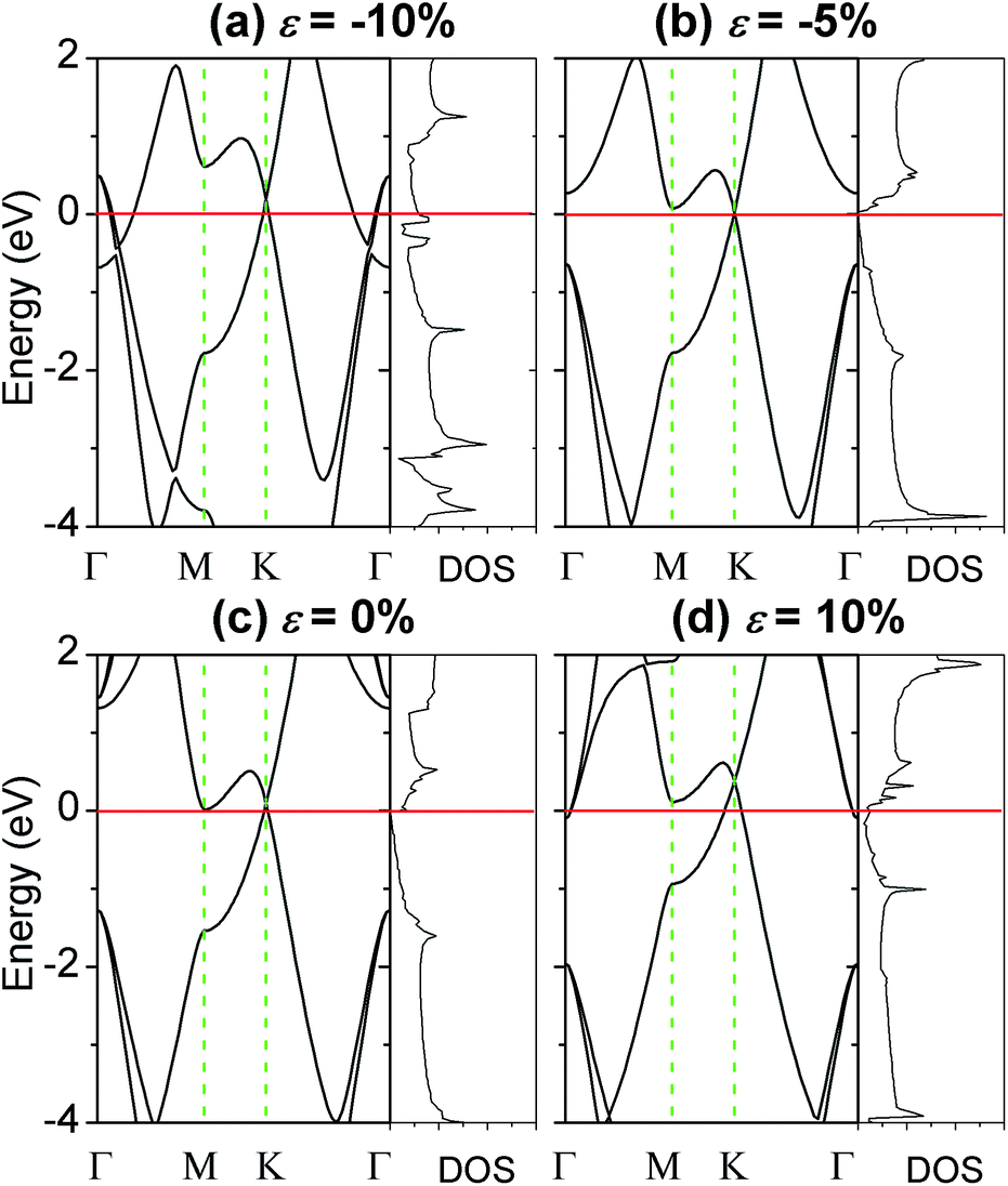 | ||
| Fig. 2 The band structures and total density of states (DOS) of BeB2 monolayer under isotropic strains ε = −10%, −5%, 0% and 10%. | ||
 | ||
| Fig. 3 The projected densities of states (PDOS) of Be and B atom for BeB2 monolayer under isotropic strains (a) ε = 0% and (b) ε = −5%. | ||
Different change of band structure was observed when compressive strain was applied. As shown in Fig. 2b, the π* band shifted down a little at K point, while it shifted in the opposite direction at M point under strain ε = −5%. Interestingly, under this strain, the metallic BeB2 monolayer became a semimetal with zero density of states (DOS) at Fermi level (seen in Fig. 2b and 3b). It would be discussed in details in the next paragraph. Our results suggested that the semimetallic nature of BeB2 monolayer would be maintained under strain ε = −6∼–4%. The range was much smaller than that of graphene (about −9.8∼8.4%),15 indicating that the semimetallic nature of compressed BeB2 monolayer was more sensitive than that of graphene. When the compressive strain increased to −10%, the π* band at M point still shifted upwards, while some bands crossed Fermi level along the Γ–M line. The π* band at K point shifted upwards as compensation for electron, therefore the BeB2 monolayer turned out to be metallic again under larger compressive strain.
Then we focused on BeB2 monolayer under isotropic strain ε = −5%, the zero-band-gap semimetallic system. It should be noted that a benchmark calculation suggested that the dipole correction was negligible for our system (as shown in Fig. S1 in the ESI†), so all these calculations were carried out without dipole correction. The Dirac point of semimetallic BeB2 monolayer still lied at the Fermi level in the cases of LDA and HSE06 functionals, though the introduction of non-local Fock exhange made some bands broader (as shown in Fig. S2†). The highest valence and lowest conduction bands of the BeB2 monolayer were shown in Fig. 4. A Dirac point was observed obviously at the Fermi level, however, different to graphene, there were many single cones near the Fermi level. The orthographic view of the lowest conduction band was shown in Fig. 4b, which showed that only the cone at K point (in a black circle) touched the Fermi level. The valence and conduction bands of BeB2 monolayer in the vicinity of the Dirac point (shown in Fig. 4c) were very similar to that of graphene. These bands exhibited a linear dispersion in both kx and ky directions, which suggested zero effective mass of the mobile electron. To examine the carrier mobility around the Dirac cones, the Fermi velocity was evaluated by linear fitting the first derivatives of the band energies near Dirac point. The slope of the valence and conduction bands near Dirac cone was about ±35.5 eV Å, equivalent to a Fermi velocity vF = E/ħk = 0.857 × 10⁶ m s−1, where ħ is reduced Planck's constant. The Fermi velocity was a little smaller than that of graphene (0.95 × 10⁶ m s−1),30 but much larger than that of α-graphyne (0.676 × 10⁶ m s−1).4 It should be noted that the Fermi velocity at DFT Kohn–Sham level was usually underestimated in comparison with corresponding GW value and experimental value.30 In other words, the experimental Fermi velocity of semimetallic BeB2 monolayer should be larger than predicted.
 | ||
| Fig. 4 (a) The perspective view of highest valance band and lowest conduction band of BeB2 monolayer under isotropic strain ε = −5%. (b) The orthographic view of the lowest conduction band. (c) Dirac cone formed by the valence and conduction bands in the vicinity of the Dirac point. | ||
In order to explore the physical origin of the Dirac cone under ε = −5%, the band decomposed charge density at Dirac point was plotted in Fig. 5a. The charge density of the highest valence band and the lowest conduction band at Dirac point were displayed in green and red, respectively. As shown in Fig. 5a, the charge density distribution was derived from out-of-plane pz orbitals and exhibited π bonding character, which was responsible for the Dirac cone. The electron localization function (ELF) distribution with an isovalue of 0.75 was displayed in Fig. 5b. It showed ionic bonding between Be and boron atoms and strong covalent σ bonding derived from in-plane sp2 hybridization between boron atoms. As shown in Table 1, Bader charge analysis showed that charge of about 1.6e transferred from Be atom to boron atoms under ε = 0% and the value kept almost a constant whenever a compressive or tensile strain was applied. In the mean while, two boron atoms gained about 1.0e and 0.6e, indicating that they were nonequivalent and formed two interpenetrating triangular sublattices. Therefore, boron hexagonal lattice with excess electron mimicked the Dirac cone of graphene when B–B bond distance was appropriate.
 | ||
| Fig. 5 (a) The band decomposed charge density distribution of BeB2 monolayer at Dirac point under isotropic strain ε = −5%. (b) The electron localization function (ELF) distribution with an isovalue of 0.75 for BeB2 monolayer under ε = −5%. | ||
Except for isotropic strain, we also studied the effect of uniaxial strain on the electronic properties BeB2 monolayer. The primitive cell was stretched or compressed perpendicular to B–Be bonds (along x-axis in Fig. 1a) or parallel to B–Be bonds (along y-axis in Fig. 1a) with other lattice constants unchanged. The definition of uniaxial strain εx or εy was similar to that of isotropic strain, while the parameter a was replaced by the periodicity length along corresponding strain direction.
The total density of states (DOS) of BeB2 monolayer under different uniaxial strain εx or εy were displayed in Fig. 6. As shown in Fig. 6, the metallic nature of BeB2 monolayer was maintained when tensile strain was applied, no matter whether it was along x-axis or y-axis. This trend was in accordance with that under isotropic strain. Interestingly, the BeB2 monolayer would become narrow-gap semiconductor when uniaxial compressive strain was applied to the system, which suggested that symmetry breaking under uniaxial compressive strain opened band gap at the Fermi level. The gaps were 0.05 eV and 0.14 eV under εx = −5% and εy = −5%, respectively.
 | ||
| Fig. 6 The total density of states (DOS) of BeB2 monolayer under different uniaxial strains (a) εx perpendicular to B–Be bonds and (b) εy parallel to B–Be bonds. | ||
How to apply strain on the monolayer may be a challenge. It was reported that the Dirac cone of silicone survived when it was supported by Ag (111) surface, though its lattice constant was 4% smaller than the theoretical one.31 It indicated that there would exist appropriate substrate, which compressed the lattice of BeB2 monolayer with Dirac cone survived.
Conclusions
First principles calculations were carried out to investigate the effect of isotropic and uniaxial strains on the geometry, band structure and electronic properties of BeB2 monolayer. Our results suggested that the distance between Be atom and boron base plane decreased almost linearly with the increase of isotropic strain. Most strikingly, the metallic BeB2 monolayer could transform to semimetal with a Dirac point at the Fermi level when the lattice parameters were isotropically compressed by about 5%, while it would become metallic again under larger compression. The Fermi velocity of semimetallic BeB2 monolayer was 0.857 × 10⁶ m s−1, just a little smaller than that of graphene. To our knowledge, the compressed BeB2 monolayer was the first 2D semimetal with triangular lattice. The charge transfer from Be atom to B atoms would keep almost a constant whenever an isotropic compression or stretch was applied. Therefore, the boron hexagonal lattice with excess electron mimicked the Dirac cone of graphene when B–B bond distance was appropriate. Furthermore, it was found that uniaxial compressive strain opened band gap in BeB2 monolayer, while uniaxial tensile strain kept it metallic. Our study expands the Dirac systems and provides a new insight to explore novel semimetallic materials.Acknowledgements
This work was supported by the National Natural Science Foundation of China (no. 21373130, 11302121 and 21473106). Yuewen Mu gratefully acknowledges the support of a start-up fund from Shanxi University. The calculations were performed using supercomputers at the Network Center and Institute of Molecular Science, Shanxi University.Notes and references
- K. S. Novoselov, D. Jiang, F. Schedin, T. J. Booth, V. V. Khotkevich, S. V. Morozov and A. K. Geim, Proc. Natl. Acad. Sci. U. S. A., 2005, 102, 10451–10453 CrossRef CAS PubMed.
- Y. Zhang, Y.-W. Tan, H. L. Stormer and P. Kim, Nature, 2005, 438, 201–204 CrossRef CAS PubMed.
- S. Cahangirov, M. Topsakal, E. Aktürk, H. Şahin and S. Ciraci, Phys. Rev. Lett., 2009, 102, 236804 CrossRef CAS.
- D. Malko, C. Neiss, F. Viñes and A. Görling, Phys. Rev. Lett., 2012, 108, 086804 CrossRef.
- Y. Ding and Y. Wang, J. Phys. Chem. C, 2014, 118, 4509–4515 CAS.
- X.-F. Zhou, X. Dong, A. R. Oganov, Q. Zhu, Y. Tian and H.-T. Wang, Phys. Rev. Lett., 2014, 112, 085502 CrossRef.
- H. Şahin, S. Cahangirov, M. Topsakal, E. Bekaroglu, E. Akturk, R. T. Senger and S. Ciraci, Phys. Rev. B: Condens. Matter Mater. Phys., 2009, 80, 155453 CrossRef.
- P. Zhang and V. Crespi, Phys. Rev. Lett., 2002, 89, 056403 CrossRef.
- D. E. Sands, C. F. Cline, A. Zalkin and C. L. Hoenig, Acta Crystallogr., 1961, 14, 309–310 CrossRef CAS.
- T. Mori, J. Mater. Sci. Lett., 2001, 20, 1857–1858 CrossRef CAS.
- C. L. Kane and E. J. Mele, Phys. Rev. Lett., 2005, 95, 226801 CrossRef CAS.
- S. Murakami, N. Nagaosa and S.-C. Zhang, Phys. Rev. Lett., 2004, 93, 156804 CrossRef.
- V. M. Pereira and A. H. Castro Neto, Phys. Rev. Lett., 2009, 103, 046801 CrossRef.
- S.-M. Choi, S.-H. Jhi and Y.-W. Son, Phys. Rev. B: Condens. Matter Mater. Phys., 2010, 81, 081407 CrossRef.
- G. Gui, J. Li and J. Zhong, Phys. Rev. B: Condens. Matter Mater. Phys., 2008, 78, 075435 CrossRef.
- Z. H. Ni, T. Yu, Y. H. Lu, Y. Y. Wang, Y. P. Feng and Z. X. Shen, ACS Nano, 2008, 2, 2301–2305 CrossRef CAS PubMed.
- B. Verberck, B. Partoens, F. M. Peeters and B. Trauzettel, Phys. Rev. B: Condens. Matter Mater. Phys., 2012, 85, 125403 CrossRef.
- X. Zhong, Y. Yap, R. Pandey and S. Karna, Phys. Rev. B: Condens. Matter Mater. Phys., 2011, 83, 193403 CrossRef.
- P. Johari and V. B. Shenoy, ACS Nano, 2012, 6, 5449–5456 CrossRef CAS PubMed.
- B. Huang, J. Yu and S.-H. Wei, Phys. Rev. B: Condens. Matter Mater. Phys., 2011, 84, 075415 CrossRef.
- G. Kresse and J. Furthmuller, Phys. Rev. B: Condens. Matter Mater. Phys., 1996, 54, 11169–11186 CrossRef CAS.
- G. Kresse and J. Hafner, J. Phys.: Condens. Matter, 1994, 6, 8245–8257 CrossRef CAS.
- P. E. Blochl, Phys. Rev. B: Condens. Matter Mater. Phys., 1994, 50, 17953–17979 CrossRef.
- G. Kresse and D. Joubert, Phys. Rev. B: Condens. Matter Mater. Phys., 1999, 59, 1758–1775 CrossRef CAS.
- J. P. Perdew, K. Burke and M. Ernzerhof, Phys. Rev. Lett., 1996, 77, 3865–3868 CrossRef CAS.
- A. V. Krukau, O. A. Vydrov, A. F. Izmaylov and G. E. Scuseria, J. Chem. Phys., 2006, 125, 224106 CrossRef PubMed.
- H. J. Monkhorst and J. D. Pack, Phys. Rev. B: Solid State, 1976, 13, 5188–5192 CrossRef.
- A. Togo, F. Oba and I. Tanaka, Phys. Rev. B: Condens. Matter Mater. Phys., 2008, 78, 134106 CrossRef.
- I. I. Tupitsyn, I. I. Lyakhovskaya, M. S. Nakhmanson and A. S. Sukhikh, Phys. Solid State, 1975, 16, 2015 Search PubMed.
- P. E. Trevisanutto, C. Giorgetti, L. Reining, M. Ladisa and V. Olevano, Phys. Rev. Lett., 2008, 101, 226405 CrossRef.
- L. Chen, C.-C. Liu, B. Feng, X. He, P. Cheng, Z. Ding, S. Meng, Y. Yao and K. Wu, Phys. Rev. Lett., 2012, 109, 056804 CrossRef.
Footnote |
| † Electronic supplementary information (ESI) available. See DOI: 10.1039/c4ra14684k |
| This journal is © The Royal Society of Chemistry 2015 |