Ratan Debnath*a,
Ting Xieab,
Baomei Wenac,
Wei Lide,
Jong Y. Haaf,
Nichole F. Sullivanc,
Nhan V. Nguyend and
Abhishek Motayedaf
aMaterials Science and Engineering Division, Material Measurement Laboratory, National Institute of Standards and Technology, Gaithersburg, MD 20899, USA. E-mail: ratan.debnath@nist.gov
bDepartment of Electrical and Computer Engineering, University of Maryland, College Park, MD 20742, USA
cN5 Sensors Inc., Rockville, MD 20852, USA
dSemiconductor and Dimensional Metrology Division, Physical Measurement Laboratory, National Institute of Standards and Technology, Gaithersburg, MD 20899, USA
eKey Laboratory for the Physics and Chemistry of Nano Devices, Peking University, Beijing, China
fInstitute for Research in Electronics and Applied Physics, University of Maryland, College Park, MD 20742, USA
First published on 20th January 2015
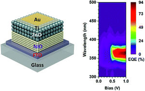
This paper presents a high efficiency heterojunction p-NiO/n-ZnO thin film ultraviolet (UV) photodetector (PD) fabricated on conductive glass substrates. The devices are fabricated by using a simple spin-coating layer-by-layer method from precursor solutions. Photodiodes show good photoresponse and quantum efficiency under UV illumination. With an applied reverse bias of 1 V, the devices show maximum responsivity and detectivity of 0.28 A W−1 and 6.3 × 10¹¹ Jones, respectively, as well as high gain with external quantum efficiency (EQE) of over 90%. By employing ultrathin Ti/Au as top UV transparent metal contacts, this architecture allows the PDs to be illuminated either through glass or metal side. Laser beam induced current is used to examine the local variation of EQE providing information on the photoresponse behavior within the device. Optical properties of NiO and ZnO deposits have also been explored.
In this paper, we have fabricated UV PDs from transparent layers of NiO and ZnO spin-coated from a sol–gel solution. The devices are fabricated on low-cost fluorine-doped tin oxide (FTO) coated glass substrates rather than indium-doped tin oxide, which allows annealing at high temperature although they are processed at relatively low temperature. UV transparent top metal contacts are engineered allowing illumination of devices through both the glass/FTO and top metal contacts. Finally, the performance of the PDs are measured to demonstrate high external quantum efficiency (EQE) and responsivity.
:
MEA was maintained at 1
:
1 in the solution. The dissolved precursors were magnetically stirred at 50 °C for 2 hours in a water bath and then filtered with a 0.45 μm filter.
An integrated HORIBA Jobin Yvon's LabRAM 800HR bench-top system† was used for Raman spectroscopy (Laser Quantum DPSS, 532 nm) measurements with laser spot sizes of ≈1 μm. The local EQE measurements were collected using the same Raman microscope system equipped with a laser (Kimmon He–Cd, 325 nm). The beam was turned on a minimum of 20 min prior to use in order to ensure power stability during measurements. Vacuum ultraviolet variable angle ellipsometry (VUV-VASE) measurements were performed to determine the dielectric functions of the films from which optical band gaps were extracted by employing Tauc plots.35 Currents were monitored chronopotentiometrically with a CH instruments potentiostat connected to the device by micromanipulator probes. The laser beam passed through a neutral density filter and 15× UV objective for focusing, and the light intensity at the device was measured with a Thor Laboratories PM100D laser power meter immediately after device measurements. Measured laser output power at the sample for these conditions was on the order of 6.5 μW. Total uncertainties on stated power are ± 3% based on the measured change of beam intensity over the duration of the mapping experiments.
For mapping, the sample was scanned using a step size of 20 μm resolution to cover a 400 μm × 400 μm area. On the basis of an approximate beam diameter of 20 μm obtained from visual examination, local EQE in the device was estimated and thus the absolute values in the EQE maps reported here should not be considered directly comparable to standard EQE measurements.
Fig. 2a shows the Tauc plot of the thin films which is a linear relationship of (αhν)2 vs. photon energy where α is the absorption coefficient and hν is the photon energy. The optical band gaps are deduced from a linear fit to the near band gap spectral region and found to be ≈3.68 eV and ≈3.24 eV for NiO and ZnO, respectively. Thus, both films are highly transparent in the visible range making them suitable for UV PDs. The micro-Raman spectra in Fig. 2b were recorded using 532 nm excitation wavelength at room temperature. The bands observed at ≈(460.3 ± 0.7) cm−1 and ≈(562.3 ± 0.5) cm−1 can be ascribed to the transverse optical (TO) and longitudinal optical (LO) phonon modes of NiO, respectively. The peaks at ≈(784.6 ± 0.5) cm−1 and ≈(1094.4 ± 0.3) cm−1 correspond to 2TO and 2LO combination phonon modes. All these are in good agreement with the reported values of NiO.36,37 Similarly, the peaks at ≈(431.1 ± 0.1) cm−1 and ≈(375.5 ± 0.1) cm−1 are close to Ehigh2 and A1(TO) of ZnO.38 XRD patterns of the films are shown in Fig. 2c. All diffraction peaks can be indexed to the cubic NiO (JCPDS-78-0643) or hexagonal ZnO structure (JCPDS 36-1451). The broad diffraction peaks are consistent with the small grain size and/or high defect density of material processed relatively at low temperature.
The band diagrams of the NiO/ZnO interface at steady state and under reverse bias are plotted in Fig. 3a using SCAPS-1D simulator.39 At equilibrium, there is a space-charge region at the interfaces due to the diffusion of electrons and holes, and a built-in electrical field is created that assists in separation of electrons and holes. Under reverse bias, the depletion region of the junction increases and a very small net current flow across the device is expected. The I–V curve of the NiO/ZnO heterojunction diode reveals the anticipated rectifying behavior and exhibits a rectification ratio of ≈2200 at ± 1 V in the dark (Fig. 3b). Under UV illumination, current enhancement is observed under reverse bias. The increased currents result from the photogenerated carries within the junction. The photogenerated electrons are transported through the ZnO layer to the Ti/Au cathode and the holes are transported from the NiO to the FTO anode. The photoresponse factor (S) of the PD is defined as
Fig. 4a shows the EQE of a NiO/ZnO device under applied reverse bias. The illumination is through the FTO/glass side and the spectral response is measured by scaling the measured photocurrent with that of a Si photodetector, given nominally identical illumination. At a reverse bias of 1 V, the maximum EQE at 365 nm reaches to ≈93% (Fig. 4a). The EQE of the detector is limited by the UV cut-off wavelength of the FTO anode and thus it gradually decreases to ≈0.3% at 320 nm. The responsivity (Rλ) which is the ratio of photocurrent and light intensity is approximately ≈0.28 A W−1 at 365 nm (Fig. 4b). The heterojunction device exhibits excellent UV-selective sensitivity with a UV-to-visible rejection ratio (Rλ=365 nm/Rλ=550 nm) approaching ≈1500. The specific detectivity (D*), which is another figure of merit can be calculated assuming the dark current to be the major source of shot noise using the expression:
The device architecture also allows illumination through the Ti/Au ultrathin metal contacts permitting UV transmission as reported for other metal.43 A PD response from this configuration is shown in Fig. 5a. The EQE reaches ≈57% at 355 nm and the corresponding Rλ and D* estimated to be 0.18 A W−1 and 4.1 × 10¹¹ Jones at 0.8 V, respectively. Although ultrathin Ti/Au contacts likely absorb some UV light, but they are still more transparent as compared to FTO electrode in the UV regime (below 330 nm) and hence, the response of the PD is extended up to 300 nm. Overall, the figures of merit are quite reasonable as compared to those for bottom illumination.
![]() | ||
| Fig. 5 (a) Measured EQE of the same device shown in Fig. 4a as a function of applied reverse bias. Here, light is illuminated through Ti/Au contact. The EQE reaches to a maximum value of 55% at 355 nm under 0.8 V. (b) Large area (400 μm × 400 μm) EQE map of the device at zero bias. The photoresponse from the device can be seen with some variation across the measured area of the specimen. (c) Time-resolved photocurrent response to a 20 s light pulse from 325 nm He–Cd laser demonstrating the characteristics transient response of the semiconductors. Dark currents have been subtracted. | ||
In order to assess the spatial variation of device performance under UV illumination, we have mapped the photoresponse with a piezoelectric stage and a focused He–Cd 325 nm, 6.5 μW laser beam. The EQE estimated from the current under short circuit conditions (i.e., under zero bias) indicates ≈30% relative variation across the surface of this heterojunction device suggesting spatial variation of recombination (Fig. 5b). When the device is operated under reverse bias, there is significant increase of EQE as seen in Fig. 4a and 5a. It has been reported that NiO films fabricated this way contain Ni2O3 or Ni(OH)2 as well as NiO when annealed at lower temperature.25 That can act as trap sites in the NiO film. The gain in this photodiode has been correlated with the interfacial trap-controlled charge injection suggesting the annealing temperature plays a crucial role controlling defects and deviation from stoichiometry.
Fig. 5c shows the transient response of the fabricated photodetectors during 325 nm laser excitation switching. The photocurrent increases rapidly upon exposure to UV radiation and stays essentially constant during the UV exposure. The current responds far more slowly to the pre-exposure value after illumination is turned off. The rise time (tr) for the photocurrent to reach 90% of its maximum value, is approximately 0.28 s. The decay time (td) for the photocurrent to decrease to 10% of the initial value, is 5.4 s. The values of tr and td are as good or better than, other reported oxide based PDs.40 The slow UV response and recovery can be attributed to the oxygen adsorption and desorption process.13,44,45 In the dark, oxygen molecules adsorb on the ZnO surface, capturing free electrons from the n-ZnO[O2(g) + e− → O2−(ad)]. As a consequence, a low-conductivity depletion layer is created near the surface. When the device is illuminated by UV light having photon energies exceeding the band gap of the semiconductor, electron–hole pairs are generated. These photo-generated holes migrate to the surface and either discharge the adsorbed oxygen ions through surface electron–hole recombination to produce photo-desorbed oxygen gas [O2−(ad) + h+ → O2(g)] or get trapped on the surface resulting in increased free carrier concentration and reduced depletion width. The unpaired electrons accumulate until adsorption and desorption of O2 reaches in a steady state. Thus the current will keep on rising until it is saturated by the UV illumination. This hole-trapping mechanism can augment the traps residing in the semiconductor and enhance the photoresponse. When the UV illumination is turned off, holes recombine with the unpaired electrons, while oxygen gradually reabsorbs in the surface resulting in a slow current decay. The performance of PDs in this work and some previously reported data are summarized in Table 1 for comparison.
| PD Architecture | Bias (V) | EQE (%) | Rλ (A W−1) | D* (Jones) | tr (s) | td (s) | Ref. |
|---|---|---|---|---|---|---|---|
| Ni–NiO–ZnO–ITO | 5 | 18 | — | — | — | 37 | 23 |
| In–ZnO–NiO–Au | 0 | — | 0.493 m | — | 10 μ | 30.3 μ | 47 |
| FTO–ZnO–NiO–Ag | 3 | — | 3.2 | — | — | 30 | 48 |
| ITO–NiO–ZnO–Al | 1 | 189 | 10.2 | 1 × 10¹² | 0.2 | 0.18 | 25 |
| ITO–NiO–ZnO–Al | 5 | 88 | 21.8 | 1.6 × 10¹² | — | — | 24 |
| FTO–NiO–ZnO–Ti–Au | 1 | 94 | 0.28 | 6.3 × 10¹¹ | 0.28 | 5.4 | This work |
Other opportunities to explore these ideal TMO systems exist including investigation of materials properties and device performance under various environments. This may include UV ozone treatment on those oxide films, including its effect on oxygen vacancies as well as the change in metal-oxide work function as reported in the past.46 This might assist the metal–semiconductor junction to extract the electron–holes to their respective contacts. Such treatment might also allow lowering the processing temperatures, similar to those for polymer solar cells,46 congenial to fabrications of PDs on flexible substrates. Due to the ease of cost-effective solution-processing, one might also tune the bandgap by mixing with other appropriate oxides enabling devices with photodetection capability over a larger UV range.
Footnote |
| † Certain commercial equipment, instruments, or materials are identified in this paper in order to specify the experimental procedure adequately. Such identification is not intended to imply recommendation or endorsement by the National Institute of Standards and Technology, nor is it intended to imply that the materials or equipment identified are necessarily the best available for the purpose. |
| This journal is © The Royal Society of Chemistry 2015 |