The effect of the selenization process on grain size and performance of CuIn(Sx,Se1−x)2 counter electrodes
Yan-zhu Zhang,
Huan-huan Li,
Zheng-ji Zhou*,
Dong-xing Kou,
Wen-hui Zhou and
Si-xin Wu*
The Key Laboratory for Special Functional Materials of MOE, Henan University, Kaifeng, 475004, P. R. China. E-mail: zzj@henu.edu.cn; wusixin@henu.edu.cn; Fax: +86-371-23881358; Tel: +86-371-23881358
First published on 9th January 2015
Abstract
CuIn(Sx,Se1−x)2 thin films were fabricated using S2− capped CuInS2 nanoparticles and a post-selenizing process. The different thermal annealing technologies in selenization resulted in obvious distinction in CuIn(Sx,Se1−x)2 grain size and degree of crystallinity. The nanoparticle-derived CuIn(Sx,Se1−x)2 thin films were used as counter electrodes in dye-sensitized solar cells and detailed analyses of the counter electrodes using current–voltage (J–V), cyclic voltammetry (CV), as well as electrochemical impedance spectroscopy (EIS) were conducted to investigate the influence of the grain size and crystallinity on the catalytic and electrical conductivity properties of the CuIn(Sx,Se1−x)2 thin films.
Introduction
Dye-sensitized solar cells (DSSCs), as a special type of photo-electrochemical solar cells, have attracted widespread attention over the past two decades on account of their low cost production, easy fabrication and high power conversion efficiency (PCE).1–3 A PCE of 13% has been achieved through the molecular engineering of porphyrin sensitizers in co-based electrolyte DSSC, which made it promising in commercialization.3 In principle, a standard DSSC is made up of three key constituents: a dye-sensitized TiO2 photoanode, an electrolyte with trriodide/idodide redox couple (I3−/I−) and a counter electrode (CE). The traditional CE is composed of Pt materials, due to its great electrocatalytic activity for the I3−/I− reaction as well as high conductivity. However, Pt is a noble metal, which is relatively expensive and scarce in nature. The large-scale production of Pt may be restricted owing to its limited supply. In this regard, it is highly necessary to develop new low-cost Pt-free CE catalytic materials with high electrical conductivity and superior catalytic activity. Till now, carbon materials,4–7 transition metal compounds (TMCs),8–10 conductive polymers11–14 have been proposed as substitutes to the Pt CE in DSSCs.Among the multifarious substitutes, transition metal chalcogenides such as Co0.85Se,15 NiSe2,16 CoSe,17 NbSe2![[thin space (1/6-em)]](https://www.rsc.org/images/entities/char_2009.gif) 18 have drawn enormous attention due to their distinctive electronic properties, interesting chemical behaviors and a wide variety of potential applications. Besides the binary chalcogenides, ternary and quaternary chalcogenides, CuInS(e)2 or Cu2ZnSnS(e)4, for example, were also introduced into DSSCs as CE catalysts, which displayed much higher efficiency than Pt.19,20 Moreover, multi-elemental chalcogenides CE derived from nanoparticle allows the adoption of ultra-large-scale and potentially low cost production techniques which is considered to be one of the most promising alternatives.
18 have drawn enormous attention due to their distinctive electronic properties, interesting chemical behaviors and a wide variety of potential applications. Besides the binary chalcogenides, ternary and quaternary chalcogenides, CuInS(e)2 or Cu2ZnSnS(e)4, for example, were also introduced into DSSCs as CE catalysts, which displayed much higher efficiency than Pt.19,20 Moreover, multi-elemental chalcogenides CE derived from nanoparticle allows the adoption of ultra-large-scale and potentially low cost production techniques which is considered to be one of the most promising alternatives.
For the nanoparticle-based approach to fabricate CE films, nanocrystals synthesis and post-thermal annealing process can play an important role in the structure and photoelectrical properties of the electrode.20–22 Previously, we have synthesised surfactant-free CuInS2 (CIS) nanocrystals by displacing long insulating organic capping ligands with inorganic ions S2− and found the electrical conductivity and electrocatalytic activity of CIS nanocrystals CE were sharply enhanced due to the improved interparticle coupling after ligand exchange.23 Another key strategy to improve the performance of nanocrystalline film is the subsequent sulfuration or selenization process, which can not only change the composition and morphology of the film, but also the degree of crystallinity and then the photoelectrical behavior will be evolved.24–29
In this manuscript, surfactant-free CIS nanocrystals were used to prepare the precursor films and two different thermal annealing processings were employed to selenize the nanocrystalline films. The effect of heating rates in selenization on the morphology and structure of the CuIn(Sx,Se1−x)2 (CISSe) thin films was studied. Furthermore, the obtained CISSe thin films were used as CEs in DSSCs, the relationship between grain size and crystallinity of CISSe films with the electrocatalytic activity and electrical conductivity properties of the CISSe CEs was discussed.
Experimental section
Materials
Copper(I) chloride, indium acetate, ammonium sulfide aqueous solution (20%)[(NH4)2S], 1-dodecanethiol (DDT) and octadecene (ODE) were purchased from Alfa Aesar. N-Hexane, methanamide (formamide), toluene, ethanol were purchased from Tianjin Chemical Reagents Co. All the reagents were used as received without further purification. FTO coated glass (F: SnO2, 14 Ω sq−1, Nippon Sheet Glass Group, Japan) were thoroughly washed with a mixed solution of deionized water, acetone, and 2-propanol (volume ratios of 1![[thin space (1/6-em)]](https://www.rsc.org/images/entities/char_2009.gif) :
:![[thin space (1/6-em)]](https://www.rsc.org/images/entities/char_2009.gif) 1
1![[thin space (1/6-em)]](https://www.rsc.org/images/entities/char_2009.gif) :
:![[thin space (1/6-em)]](https://www.rsc.org/images/entities/char_2009.gif) 1) under sonication for 60 min.
1) under sonication for 60 min.
Synthesis of surfactant-free CIS nanoparticles
The experimental details of preparing surfactant-free CIS nanoparticles can be found in our previous report.23 Briefly, 0.2 mmol indium acetate and 0.2 mmol copper(I) chloride were dispersed in the blended solution of 0.5 mL DDT and 5 mL ODE in a three-necked flask. The mixture was degassed for 5 min and filled with argon three times. Then the suspension was heated to 100 °C and kept for 10 min until a clear solution was formed. Subsequently, the precursor solution was heated up to 240 °C and kept for 1 h. Finally the flask was cooled to room temperature, the precipitates were separated by centrifugation, washed with hexane and acetone for several times and dried at vacuum oven.The surfactant-free CIS nanocrystals were synthesized by replacing organic capping ligands with inorganic ions S2−. For a typical ligand exchange using S2− ions, 10 mL of CIS nanocrystals solution (2 mg mL−1) was mixed with 10 mL of (NH4)2S solution (20 mL mL−1). The mixture was stirred for about 2 h leading to a complete phase transfer of CIS nanocrystals from hexane to the formamide phase.
CIS thin film deposition and selenization process
S2− capped CIS nanocrystals were combined with formamide to form a uniform nano-particle “ink”. 150 μL CIS nanocrystal “ink” was drop-casted onto the cleaned FTO glass substrate (1.5 × 2 cm2). The CIS nanocrystal thin films were formed by eliminating the formamide at 80 °C for overnight. Then the obtained films were selenized by rapid thermal process (RTP) and conventional thermal process (CTP) at 500 °C for 30 min, respectively. The RTP employed here was conducted by preheating a tube furnace to the desired temperature and then introducing a graphite box which contained the CIS films and selenium pellets (60 mg). After selenization for 30 min, the furnace was opened and cooled naturally to room temperature. The CTP was carried out by loading the preheated films and selenium pellets into a tube furnace, followed by several pump/purge cycles to remove the air, the furnace was heated to the desired temperature at the rate of 10 °C min−1 under argon flow. Finally, the films were slowly cooled down to room temperature.Characterizations
The morphology of the CISSe thin films were investigated using field emission scanning electron microscope (FESEM, NOVA NANOSEM 450 at 5 kV). The crystal structure was determined by X-ray diffraction (XRD, Philips X′ PertPro, Cu-Kα: λ = 0.154056 nm). Cyclic voltammetry (CV) was carried out in a three-electrode system in an acetonitrile solution of 0.1 M LiClO4, 10 mM LiI, and 1 mM I2 at a scan rate of 50 mV s−1. Electrochemical impedance spectroscopy (EIS) was performed in dark using an impedance measurement unit (ZAHNER-elektrik IM6) in the frequency range of 0.1–105 Hz with ac amplitude of 10 mV.The photocurrent–voltage (J–V) measurements were taken on a digital source meter (Keithley 2400, computer-controlled) with the device under AM 1.5 G spectra, which was produced by a solar simulator (Newport, Oriel class A, SP91160A, USA). The light power density was calibrated against a Si-based reference cell (Hamamatsu S1133) to accurately simulate the full-sun intensity (100 mW cm−2). TiO2 photoanodes with an effective area of 0.4 × 0.4 cm2 were immersed overnight in 0.3 mM ethanolic solution of dye N-719 (Solaronix) at room temperature to absorb the dye molecule. The sandwich-type solar cell was assembled by placing the counter electrode on N-719 dye sensitized photoelectrode, and clipped together as an open cell for measurements. The cell was then filled with a liquid electrolyte composed of 0.1 M anhydrous LiI, 0.12 M I2, 1.0 M 1,2-dimethyl-3-n-propylimidazolium iodide (DMPII) and 0.5 M tert-butylpyridine in dehydrated acetonitrile by capillary force.
Results and discussion
FESEM images of the CIS nanocrystal films selenized by RTP and CTP were shown in Fig. 1. From the planar (Fig. 1a) and cross-sectional (Fig. 1c) FESEM micrographs of CIS films selenized by RTP, the obtained film was composed of large and densely packed grains, while the CIS nanoparticle film annealed by CTP didn't show obvious crystal regrowth, as shown in Fig. 1b and d. The large grains were formed by diffusing of cations, which spread from the interior of nanoparticle film to the surface and reacted with selenium vapor.30 It just took a few seconds for RTP to achieve the desired temperature, which would provide a sudden high energy assisting the rapid diffusion of anion and cation, thus contribute to the formation of large grains.31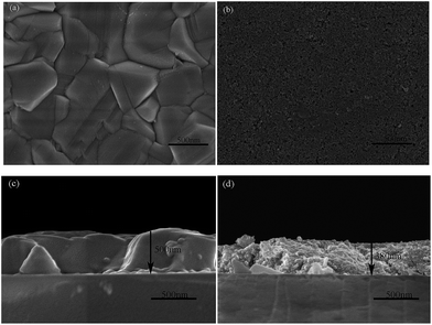 | ||
| Fig. 1 FESEM images of CIS nanocrystal films selenized by RTP (a and c) and CTP (b and d). (a and b) are the surface topography, (c and d) are cross-sectional view. | ||
It is well known that the electrical conductivity of thin films will be enhanced because of the grain growth resulted from selenization process.32 In our experiment, the resistivities of CIS nanocrystal films selenized by RTP and CTP were shown in Table 1 (the electrical resistivity measurement of CISSe films was directly carried out using the model device with a typical soda lime float glass (SLG)/CISSe/Al structure). From the data listed in the table, we can see that the resistivity of the well-crystallized CISSe film with densely packed large grains was just 1.08 Ω cm, while the value was almost 30.66 Ω cm for poor-crystallized CISSe film with fine grains. These results further confirmed that the crystal regrowth promoted by selenization by RTP would improve the crystallinity and grain size of CISSe film, consequently enhance the electrical conductivity.
| Sample | Voc (V) | Jsc (mA cm−2) | FF | η (%) | Rs (Ω cm2) | Rct (Ω cm2) | ρ (Ω cm) |
|---|---|---|---|---|---|---|---|
| Large-grain | 0.731 | 14.26 | 0.71 | 7.40 | 36.26 | 1.14 | 1.08 |
| Fine-grain | 0.714 | 12.05 | 0.71 | 6.12 | 32.99 | 1.95 | 30.66 |
| Pt | 0.706 | 11.74 | 0.73 | 6.02 | 17.36 | 2.16 | — |
XRD patterns of the CIS nanocrystal films selenized by RTP and CTP are shown in Fig. 2. The diffraction peaks of the CISSe film obtained from selenization by RTP shifted slightly to the left as compared to the film selenized by CTP, which was attributed to the expansion of unit cell after selenization. For selenizing by RTP, more S atoms were substituted by larger Se atoms. In addition, the diffraction peaks became sharp after selenization by RTP, indicating a bigger growth in the crystalline domain of grains in the well-crystallized film. This result was in line with the observations from FESEM as shown in Fig. 1. Furthermore, some minor characteristic peaks of the chalcopyrite CISSe were present in the well-crystallized film selenized by RTP, such as (101), (103), (211), and (316/332) peaks.33
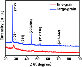 | ||
| Fig. 2 XRD patterns of the well-crystallized CISSe film with densely packed large grains and the poor-crystallized CISSe film with fine grains. | ||
The obtained CISSe films were used as the CEs in DSSCs and the effect of grain size and crystallinity of CISSe films on the performance of DSSC devices was studied. Fig. 3 shows J–V curves of DSSCs using different CISSe films and Pt as CEs. The detailed photovoltaic parameters, including the short-circuit current (Jsc), the open-circuit voltage (Voc), the fill factor (FF), and the energy conversion efficiency (η), are summarized in Table 1. The DSSC using the CIS nanocrystal film selenized by RTP as CE exhibited the best performance with an efficiency of 7.40%, an open-circuit voltage of 0.731 V, a short-circuit current density of 14.26 mA cm−2, a fill factor of 0.71. The enhancement of crystallization and grain size of CISSe films by RTP contributed a significant increase of Jsc and cell efficiency, which can be explained by the lower resistance for charge transport in the well-crystallized CISSe film with densely packed large grains.32,34 Meanwhile, it can be seen that all the DSSCs with CISSe CEs possess comparable performances to the Pt-coated CE, indicating that CISSe is an efficient alternative material and has superior electrocatalytic activity to reduce oxidized triiodide to iodide.
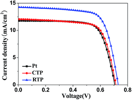 | ||
| Fig. 3 Photocurrent–voltage characteristics of DSSCs based on CISSe CEs with different crystallinity and Pt CE. | ||
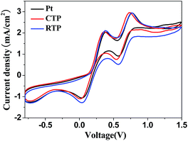
To compare the catalytic activities of CISSe CEs with different crystallinity under I−/I3− electrochemical system, CV measurement was performed. In the cyclic voltammograms (Fig. 4), there are two pairs of redox peaks for all of the CEs. The more negative pair is assigned to redox reaction (1), while the more positive one is assigned to redox reaction (2).35
| I3− + 2e− ⇌ 3I− | (1) |
| 3I2 + 2e− ⇌ 2I3− | (2) |
From CV curve, the current peak positions of the poor-crystallized CISSe CE are comparable to that of the Pt electrode, suggesting that the poor-crystallized CISSe CE possesses a similar electrocatalytic performance to the Pt electrode. However, the current density between cathodic and anodic peak of the well-crystallized CISSe CE is larger than that of the poor-crystallized CE, indicating that the redox reaction is more efficiently preceded for the well crystalline CISSe CE. Hence, the increase of crystallinity can lead to an improvement in the electrocatalytic activity of CISSe CEs.
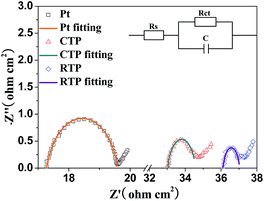
EIS measurements were conducted to further investigate the electrochemical characteristics of CISSe CEs with different crystallinity. Fig. 5 shows Nyquist plots of the symmetric configurations which were fabricated with two identical electrodes (the CISSe CEs with different crystallinity or Pt CEs) adopting the sandwich structure of CEs and electrolyte (CE/electrolyte/CE). The high-frequency (corresponding to low Z′) intercept on the Z′ axis represents the series resistance (Rs), while the semicircle in the high frequency region which stands for charge transfer resistance (Rct) corresponds to the charge-transfer ability of electrolyte/electrode interface.36 The values of Rs and Rct obtained by fitting the spectra in Fig. 5 with an EIS spectrum analyzer were summarized in Table 1. The series resistance Rs values of CISSe CE obtained from selenization by CTP is 32.99 Ω cm2. For the electrode selenized by RTP, Rs is 36.26 Ω cm2, which is a little bigger than that of CISSe CE selenized by CTP. The slightly larger Rs value of CISSe CE selenized by RTP may originate from the FTO substrate, which was some extent destroyed during the rapid and enduring heating selenization.
It is well-known that Rct is the most important parameter to demonstrate the catalytic ability of the CE. A smaller Rct facilitates electron transfer from CE to electrolyte for catalytic reduction of I3− to I− and accordingly results in less interfacial recombination.37 It can be seen that the value of Rct decreases obviously from 1.95 Ω cm2 to 1.14 Ω cm2 with the increase of the crystallinity of CISSe CEs, indicating that the well-crystallized CISSe CE with densely packed large grains has higher electrocatalytic activity and better conductivity, which is consistent with the conclusion of cyclic voltammetry. An ideal counter electrode of dye-sensitized solar cells should possess both high catalytic activity and high conductivity. Therefore, high catalytic activity for reactions between I− and I3−, good electronic conduction, high surface contact with the electrolyte are preferred characteristics for CE materials and all these factors contribute to the decrease of Rct. Although the poor-crystallized CISSe films with fine grains possess relatively high surface area which is beneficial to electrolyte penetration; however, the grain growth associated with the selenization process is known to enhance the electrical conductivity of thin films, which would promote the charge accumulating at the surface of the well-crystallized CISSe CE with densely packed large grains, subsequently speed up the reduction of I3− and I− then gradually decrease the Rct of the compact CISSe films prepared by RTP.
Conclusions
In summary, two different thermal annealing processings were employed during the selenization of surfactant-free CIS nanocrystal thin films. The influence of heating rates in selenization on the morphology and structure of the CISSe thin films was investigated. It was found that the CIS nanocrystal films selenized by RTP resulted in the larger CISSe grains with higher degree of crystallinity, while the nanoparticle-derived films annealed by CTP didn't show evident crystal regrowth. Furthermore, the obtained CISSe thin films were used as CEs in DSSCs. The well-crystallized CISSe film with densely packed large grains exhibited an impressive electrocatalytic activity for triiodide reduction. We infer that the efficient electron transport process resulted from the high crystallization is of great importance to the enhancement of photovoltaic performances of DSSCs.Acknowledgements
This project is supported by the National Natural Science Foundation of China (21203053, 21271064 and 61306016), the Joint Talent Cultivation Funds of NSFC-HN (U1204214), the Program for Changjiang Scholars and Innovative Research Team in University (PCS IRT1126) of Henan University.References
- B. O'Regan and M. Gratzel, Nature, 1991, 353, 737–740 CrossRef.
- C. T. Li, C. P. Lee, Y. Y. Li, M. H. Yeh and K. C. Ho, J. Mater. Chem. A, 2013, 1, 14888–14896 CAS.
- S. Mathew, A. Yella, P. Gao, R. Humphry-Baker, B. F. Curchod, N. Ashari-Astani, I. Tavernelli, U. Rothlisberger, M. K. Nazeeruddin and M. Gratzel, Nat. Chem., 2014, 6, 242–247 CrossRef CAS PubMed.
- A. G. Kannan, J. Zhao, S. G. Jo, Y. S. Kang and D. W. Kim, J. Mater. Chem. A, 2014, 2, 12232–12239 CAS.
- B. Lee, D. B. Buchholz and R. P. H. Chang, Energy Environ. Sci., 2012, 5, 6941–6952 CAS.
- K. Yu, Z. Wen, H. Pu, G. Lu, Z. Bo, H. Kim, Y. Qian, E. Andrew, S. Mao and J. Chen, J. Mater. Chem. A, 2013, 1, 188–193 CAS.
- H. Wang, K. Sun, F. Tao, D. J. Stacchiola and Y. H. Hu, Angew. Chem., Int. Ed., 2013, 52, 9210–9214 CrossRef CAS PubMed.
- S. Yun, M. Wu, Y. Wang, J. Shi, X. Lin, A. Hagfeldt and T. Ma, ChemSusChem, 2013, 6, 411–416 CrossRef CAS PubMed.
- H. Zhou, Y. Shi, L. Wang, H. Zhang, C. Zhao, A. Hagfeldt and T. Ma, Chem. Commun., 2013, 49, 7626–7628 RSC.
- H. M. Chuang, C. T. Li, M. H. Yeh, C. P. Lee, R. Vittal and K. C. Ho, J. Mater. Chem. A, 2014, 2, 5816–5824 CAS.
- Q. Tang, H. Cai, S. Yuan and X. Wang, J. Mater. Chem. A, 2013, 1, 317–323 CAS.
- B. He, Q. Tang, T. Liang and Q. Li, J. Mater. Chem. A, 2014, 2, 3119–3126 CAS.
- Y. Xiao, G. Han, Y. Li, M. Li and Y. Chang, J. Mater. Chem. A, 2014, 2, 3452–3460 CAS.
- T. H. Lee, K. Do, Y. W. Lee, S. S. Jeon, C. Kim, J. Ko and S. S. Im, J. Mater. Chem., 2012, 22, 21624–21629 RSC.
- F. Gong, H. Wang, X. Xu, G. Zhou and Z. S. Wang, J. Am. Chem. Soc., 2012, 134, 10953–10958 CrossRef CAS PubMed.
- F. Gong, X. Xu, Z. Li, G. Zhou and Z. S. Wang, Chem. Commun., 2013, 49, 1437–1439 RSC.
- Z. Zhang, S. Pang, H. Xu, Z. Yang, X. Zhang, Z. Liu, X. Wang, X. Zhou, S. Dong and X. Chen, RSC Adv., 2013, 3, 16528–16533 RSC.
- M. A. Ibrahem, W. C. Huang, T. W. Lan, K. M. Boopathi, Y. C. Hsiao, C. H. Chen, W. Budiawan, Y. Y. Chen, C. S. Chang, L. J. Li, C. H. Tsai and C. W. Chu, J. Mater. Chem. A, 2014, 2, 11382–11390 CAS.
- J. Yang, C. Bao, J. Zhang, T. Yu, H. Huang, Y. Wei, H. Gao, G. Fu, J. Liu and Z. Zou, Chem. Commun., 2013, 49, 2028–2030 RSC.
- X. K. Xin, M. He, W. Han, J. H. Jung and Z. Q. Lin, Angew. Chem., Int. Ed., 2011, 50, 11739–11742 CrossRef CAS PubMed.
- S. J. Yuan, Z. J. Zhou, Z. L. Hou, W. H. Zhou, R. Y. Yao, Y. Zhao and S. X. Wu, Chem.–Eur. J., 2013, 19, 10107–10110 CrossRef CAS PubMed.
- C. K. Miskin, W. C. Yang, C. J. Hages, N. J. Carter, C. S. Joglekar, E. A. Stach and R. Agrawal, Prog. Photovoltaics, 2014 DOI:10.1002/pip.2472.
- R. Y. Yao, Z. J. Zhou, Z. L. Hou, X. Wang, W. H. Zhou and S. X. Wu, ACS Appl. Mater. Interfaces, 2013, 5, 3143–3148 CAS.
- J. van Embden, A. S. Chesman, E. Della Gaspera, N. W. Duffy, S. E. Watkins and J. J. Jasieniak, J. Am. Chem. Soc., 2014, 136, 5237–5240 CrossRef CAS PubMed.
- B. D. Chernomordik, A. E. Béland, D. D. Deng, L. F. Francis and E. S. Aydil, Chem. Mater., 2014, 26, 3191–3201 CrossRef CAS.
- S. J. Park, J. W. Cho, J. K. Lee, K. Shin, J. H. Kim and B. K. Min, Prog. Photovoltaics, 2014, 22, 122–128 CAS.
- S. Ahn, Y. J. Choi, K. Kim, Y. J. Eo, A. Cho, J. Gwak, J. H. Yun, K. Shin, S. K. Ahn and K. Yoon, ChemSusChem, 2013, 6, 1282–1287 CrossRef CAS PubMed.
- A. R. Uhl, P. Fuchs, A. Rieger, F. Pianezzi, C. M. Sutter-Fella, L. Kranz, D. Keller, H. Hagendorfer, Y. E. Romanyuk, F. LaMattina, S. Yoon, L. Karvonen, T. Magorian-Friedlmeier, E. Ahlswede, D. VanGenechten, F. Stassin and A. N. Tiwari, Prog. Photovoltaics, 2014 DOI:10.1002/pip.2529.
- T. B. Harvey, I. Mori, C. J. Stolle, T. D. Bogart, D. P. Ostrowski, M. S. Glaz, J. Du, D. R. Pernik, V. A. Akhavan, H. Kesrouani, D. A. Vanden Bout and B. A. Korgel, ACS Appl. Mater. Interfaces, 2013, 5, 9134–9140 CAS.
- R. Mainz, B. C. Walker, S. S. Schmidt, O. Zander, A. Weber, H. Rodriguez-Alvarez, J. Just, M. Klaus, R. Agrawal and T. Unold, Phys. Chem. Chem. Phys., 2013, 15, 18281–18289 RSC.
- Y. Zhang, C. Liao, K. Zong, H. Wang, J. Liu, T. Jiang, J. Han, G. Liu, L. Cui, Q. Ye, H. Yan and W. Lau, J. Sol. Energy, 2013, 94, 1–7 CrossRef CAS PubMed.
- S. Riha, S. Fredrick, J. Sambur, Y. Liu, A. Prieto and B. Parkinson, ACS Appl. Mater. Interfaces, 2011, 3, 58–66 CAS.
- R. Caballero and C. Guillen, Sol. Energy Mater. Sol. Cells, 2005, 86, 1–10 CrossRef CAS PubMed.
- J. J. Scragg, T. Ericson, X. Fontané, V. Izquierdo-Roca, A. Pérez-Rodríguez, T. Kubart, M. Edoff and C. Platzer-Björkman, Prog. Photovoltaics, 2014, 22, 10–17 CAS.
- K. Imoto, K. Takahashi, T. Yamaguchi, T. Komura, J. Nakamura and K. Murata, Sol. Energy Mater. Sol. Cells, 2003, 79, 459–469 CrossRef CAS.
- Z. Zhang, X. Zhang, H. Xu, Z. Liu, S. Pang, X. Zhou, S. Dong, X. Chen and G. Cui, ACS Appl. Mater. Interfaces, 2012, 4, 6242–6246 CAS.
- F. Fabregat-Santiago, J. Bisquert, E. Palomares, L. Otero, D. B. Kuang, S. M. Zakeeruddin and M. Gratzel, J. Phys. Chem. C, 2007, 111, 6550–6560 CAS.
| This journal is © The Royal Society of Chemistry 2015 |

