Magnetic anisotropy and deep ultraviolet photoresponse characteristics in Ga2O3:Cr vermicular nanowire thin film nanostructure

Daoyou Guoab, Zhenping Wuab, Peigang Li*ac, Qianjing Wangd, Ming Leiab, Linghong Lie and Weihua Tang*ab
aSchool of Science, Beijing University of Posts and Telecommunications, Beijing 100876, China. E-mail: whtang@bupt.edu.cn; pgli@zstu.edu.cn
bState Key Laboratory of Information Photonics and Optical Communications, Beijing University of Posts and Telecommunications, Beijing 100876, China
cCenter for Optoelectronics Materials and Devices, Department of Physics, Zhejiang Sci-Tech University, Hangzhou 310018, China
dCollege of Physics and Electronic Information, Yunnan Normal University, Kunming 650500, China
eDepartment of Physics, The State University of New York at Potsdam, Potsdam, New York 13676-2294, USA

Received 4th November 2014 , Accepted 19th January 2015

First published on 19th January 2015


Abstract

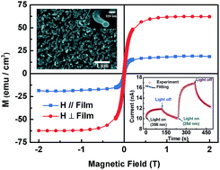
Nanostructures of magnetic doping semiconductors have attracted considerable attention due to their fantastic electronic, optical and magnetic properties as well as their unique morphology for both interconnects and functional units in fabrication of nanodevices. Herein, a Ga2O3:Cr vermicular nanowire thin film nanostructure was obtained on α-Al2O3 (0001) substrates by pulsed laser deposition. The nanostructure exhibits room temperature anisotropic ferromagnetic behavior with an easy axis perpendicular to the film plane and a Curie temperature of higher than 400 K. An obvious deep ultraviolet photoelectric response was obtained in the formed nanostructure.


Introduction

One-dimensional nanostructures, such as nanowires, nanotubes, nanorods, and nanobelts, have attracted enormous attention due to their potential applications as building blocks in nanodevices.1–3 Recently, several binary metal oxide nanowires such as ZnO, TiO2, In2O3 and SnO2 have been successfully synthesized, and their electronic and optical properties have been studied.1,4,5 β-Ga2O3, as a typical wide band gap semiconductor material, with bandgap of ∼4.9 eV and high transparency for the visible and wide range of UV down to 280 nm, is well known as a promising candidate for novel applications in optoelectronic devices such as solar-blind photodetectors, field effect transistors, gas sensors, and white light emitting devices.6–8 For instance, a multiple nanowires sensor of O2 and CO gases was fabricated with Ga2O3 nanowires synthesized by a chemical thermal evaporation method.9 A solar-blind photodetector was fabricated using β-Ga2O3 nanowires showing a high solar light rejection ratio, low photocurrent noise, and fast response.10

It is well known that the proper dopant can efficiently modify surface states, energy levels of semiconductors and transport performance of carriers for the host materials, which could enhance their electrical, optical and magnetic properties.11–14 Particularly in recent years, spintronic devices such as spin-valve transistors, non-volatile memory, logic device, ultrafast optical switches and optical isolators have stimulated great passions for realizing room-temperature ferromagnetism in nanostructured materials.15,16 The magnetic ions doped β-Ga2O3 nanostructures should be very attractive due to their fantastic electronic, optical and magnetic properties as well as unique morphology for both interconnects and functional units in nanodevices fabrication. Cr, a transition metal, is an important magnetic dopant for semiconductor, and a typical catalyst for growing nanostructures as well.17 However, the influences of Cr-doping on optoelectronic and magnetic properties are seldom reported. In this paper, we prepared the Ga2O3:Cr vermicular nanowire thin film nanostructure, and investigated the optoelectronic properties and magnetic properties.

Experimental

Ga2O3:Cr nanostructure was grown on α-Al2O3 (0001) substrates by pulsed laser deposition technique. The growing temperature was 900 °C with a pulse energy density of ∼5 J cm−2. 20 layers of Ga2O3 and Cr were deposited alternately. The Cr concentration was controlled by solely changing the laser pulse numbers during depositing the Cr layers (defined as N, N = 20 and 40 corresponding to sample Cr 20 and Cr 40 respectively). The pulse number for Ga2O3 layers was fixed at 100. The crystal structure was analyzed by a Bruker D8 Advance X-ray diffractometer (XRD) using Cu Kα (λ = 1.5405 Å) radiation. The surface morphology was characterized by a Hitachi S-4800 field emission scanning electron microscope (FE-SEM). The Cr concentration in the Ga2O3:Cr nanostructure was determined to be 1.33 at% and 2.29 at% for Cr 20 and Cr 40 respectively by the X-ray energy dispersive spectroscopy (EDS) equipped on the FE-SEM. The scanning transmission electron microscope (STEM) images and high resolution transmission electron microscope (HRTEM) images were obtained by a Tecnai G2 F30 transmission electron microscope (TEM), and the chemical compositions of single vermicular nanowire were checked by the EDS equipped on the TEM. The valences of Cr ions and element content were analyzed by X-ray photoelectron spectroscopy (XPS). Magnetic properties of the nanostructures were measured in a commercial superconducting quantum interference device (SQUID), Quantum design. To construct a metal/semiconductor/metal photodetector, radio frequency magnetron sputtering technique was used to deposit three pairs of Au/Ti interdigital electrodes on the Ga2O3:Cr nanostructure using a shadow mask. The electrode fingers were 200 μm wide, 2800 μm long, and 200 μm spacing gap. The current–voltage (IV) characters and time-dependent photoresponse of the Ga2O3:Cr nanostructure based photodetector were measured in a Keithley 2450. The time-dependent photoresponse measurement was performed with a 60 μW cm−2 excitation density UV lamp of 254 nm and 365 nm wavelengths as the light source at a constant voltage of 20 V.

Results and discussion

Fig. 1(a) shows the XRD patterns of the as-grown Ga2O3:Cr nanostructure (Cr 40). All the diffraction peaks indexed in the Fig. 1(a) exhibit a good agreement with those of the monoclinic β-Ga2O3 with lattice parameters of a = 12.23 Å, b = 3.04 Å, c = 5.80 Å and β = 103.7° (JCPDS Card no. 43-1012). Fig. 1(b) displays a typical top view FE-SEM image of the Ga2O3:Cr nanostructure (Cr 40). The vermicular nanowires with smaller aspect ratios (length-to-width ratio) are spread over the entire substrate. The average diameter of nanowires is ∼80 nm, and the average length is ∼300 nm. From the magnified image of single vermicular nanowire in the inset of Fig. 1(b), we can see that the tip of nanowire is bigger than the body. Fig. 1(c) gives the chemical compositions distribution of vermicular nanowire along the light green line with the purple arrow orientation shown in the low-magnitude plane view STEM image (the inset). The results of EDS line scan indicates that the Ga, Cr and O elements distribute uniformly. There is no difference between the tip and body of vermicular nanowire. Fig. 1(d) shows the HRTEM image of the Ga2O3:Cr vermicular nanowire thin film nanostructure. It is nano polycrystalline and in average size of ∼3.5 nm, which is in agreement with the weak diffraction peaks of XRD data. The interplaner spacings of 0.233 and 0.199 nm are corresponds to the ([3 with combining macron]11) and (600) planes of monoclinic β-Ga2O3 respectively, further demonstrating the β phase of Ga2O3.
image file: c4ra13813a-f1.tif
Fig. 1 Morphology and crystal structure of the as-grown Ga2O3:Cr vermicular nanowire thin film nanostructure of Cr 40: (a) the XRD patterns; (b) the top view FE-SEM image and the corresponding enlarged image in the inset; (c) the element distribution of the single Ga2O3:Cr vermicular nanowire as indicated in the low-magnitude plane view STEM image (inset) along the green line with the purple arrow orientation; (d) the plane view HRTEM image.

The chemical compositions and chemical states of Cr ions in the Ga2O3:Cr nanostructure were characterized using XPS. The charge-shift spectrum was calibrated using the fortuitous C 1s peak at 284.8 eV. Fig. 2(a) presents the XPS spectrum in the binding energy range of 0–1200 eV for Cr 40. Seen from Fig. 2(b), energy peak for Ga 3d is centered at 20.4 eV, which is attributable to the presence of gallium oxide and not gallium metal.18 The XPS spectra of Cr 2p core level is shown in Fig. 2(c). Based on the Gauss fitting, there is only one peak at 576.6 eV, which is corresponding to Cr3+.19 These peaks corresponding to Cr5+, Cr4+, Cr2+ and metallic Cr were not observed,20 suggesting that only Cr+3 exist in our Ga2O3:Cr nanostructure. The configuration of Cr doping Ga2O3 nanostructure should be neutral because +3Cr ions replace +3Ga ions.


image file: c4ra13813a-f2.tif
Fig. 2 (a) XPS survey spectrum of the as-grown Ga2O3:Cr vermicular nanowire thin film nanostructure of Cr 40; (b) Ga 3d in the 17–24 eV region; (c) Cr 2p3/2 in the 568–584 eV region.

Fig. 3 shows the magnetization versus magnetic field (MH) curves of the Ga2O3:Cr nanostructures at room temperature measured with the applied magnetic field parallel and perpendicular to the films. The diamagnetic contribution from the α-Al2O3 substrate was subtracted from the data. The Ga2O3:Cr vermicular nanowire thin film nanostructure displays typical hysteresis loops indicative of ferromagnetism and exhibits obvious magnetic anisotropy. For example, the saturation magnetization (Ms) of Cr 40 is 62.2 emu cm−3 for the case under perpendicular magnetic field and 18.5 emu cm−3 for the case under parallel magnetic field at 2 T. As seen in the enlarged image of MH loops in the upper left corner inset of Fig. 3, the magnetic remanence (Mr) for the applied magnetic field perpendicular to the films is also larger compare to that for the applied magnetic field parallel to the films. Magnetic parameters of Cr 40 and Cr 20 for the magnetic field parallel and perpendicular to the films are listed in Table 1. The perpendicular & parallel magnetic moments of Cr 40 and Cr 20 are 3.83 & 1.14 μB/Cr atom and 2.61 & 1.70 μB/Cr atom respectively. The magnetic moment of Cr atom in Cr-doped Ga2O3 is similar to that in Cr-doped other semiconductors, such as AlN, GaN, and ZnO.21,22 The temperature dependent magnetization (MT) properties of Cr 40 with the applied magnetic field perpendicular to the films was measured at 2 T in temperature range of 300–400 K. The MT curve shown in the lower right corner inset of Fig. 3 clearly exhibits ferromagnetic feature in the measurement temperature range, indicating that the Curie temperature is higher than 400 K.


image file: c4ra13813a-f3.tif
Fig. 3 MH curve and the corresponding enlarged image of Cr 40 (upper left corner inset) with the applied magnetic field parallel and perpendicular to the film at room temperature, and MT curve of Cr 40 at 2 T (lower right corner inset).
Table 1 Magnetic parameters for Cr 40 and Cr 20 of the Ga2O3:Cr vermicular nanowire thin film nanostructure with the applied magnetic field parallel or perpendicular to the film at room temperature
Sample Magnetic field direction Ms (emu cm−3) Mr (emu cm−3) Coercivity (Oe)
Cr 20 Perpendicular (⊥) 24.6 3.8 115
Parallel (∥) 16.0 2.3 77
Cr 40 Perpendicular (⊥) 62.2 5.7 94
Parallel (∥) 18.5 2.6 88


When discussing the origin of ferromagnetism, it should carefully consider the possible presence of a secondary phase in the films even though no secondary phases have been detected in the XRD and HRTEM measurements. The possible secondary phases are Cr metal and Cr-based oxides. Among them, only CrO2 is the ferromagnetism with a Curie temperature of 390 K.23 However, this phase could not be responsible for 400 K ferromagnetism. In fact, it can also be ruled out by the result of XPS in which Cr is only present in 3+ valence state in our samples. Other Cr-based oxides and Cr metal are all antiferromagnetic.24 It is reasonably to conclude that the room temperature ferromagnetism in the as-grown Ga2O3:Cr vermicular nanowire thin film nanostructure is intrinsic. The room temperature ferromagnetism is considered to be attributed to the substitution of Cr in the Ga positions due to the uniform distribution of Cr element in the vermicular nanowire. Origin of the anisotropic magnetization is not clear at the moment. The anisotropic behavior cannot be explained by the presence of randomly oriented ferromagnetic particles, which again indicates the intrinsic diluted ferromagnetic nature of Ga2O3:Cr nanostructure.

In order to investigate the UV photoresponse of the β-Ga2O3 thin films, a three-pair interdigital electrode was deposited through a shadow mask to serve as contact electrodes. Fig. 4(a) shows the room temperature IV characteristics of the as-grown Ga2O3:Cr nanostructure of Cr 40. The UV lamp with the wavelength of 365 nm and 254 nm were used as light sources, respectively. It can be seen clearly that the IV curve is symmetric and nearly linear both in the dark and under different illumination conditions. Such linear relationship suggests that Ohmic contacts between Ti/Au and Ga2O3 thin films.25 This is probably due to the large surface states at Ga2O3 surface so that carriers can tunnel through the barrier easily.26 Compare to that in dark, the current increases under 365 nm light and enhances obviously under 254 nm light illumination.


image file: c4ra13813a-f4.tif
Fig. 4 (a) IV characteristics curve of the Ga2O3:Cr vermicular nanowire thin film nanostructure (Cr 40) photodetector in dark, under 365 nm light, and under 254 nm light. (b) Time-dependent photoresponse of the photodetector to 365 nm and 254 nm light illumination under an applied bias of 20 V, and the corresponding exponential fitting.

Fig. 4(b) shows the time-dependent photoresponse of the photodetector to 365 nm and 254 nm illuminations by on/off switching under an applied bias of 20 V. Upon 365 nm UV illumination, the current slightly increases from approximately 10.7 nA of dark current to a non-stable value of approximately 11.9 nA extremely slow. Whereas, the current increases instantaneously to approximately 16.9 nA under 254 nm UV illumination. However, no matter for 365 nm and 254 nm UV illumination, the recovery time is long and the photocurrent decreases exponential when the light is off. We also measured multiple illumination cycles of the time-dependent photoresponse to 365 nm and 254 nm illuminations, respectively. The device exhibits a nearly identical response, indicating the high robustness and good reproducibility of the photodetector.

For more detailed comparative study of the response time, the quantitative analysis of the current rise and decay process involves the fitting of the photoresponse curve with a biexponential relaxation equation of the following type:27

 
I = I0 + Cet/τ1 + Det/τ2 (1)
where I0 is the steady state photocurrent, t is the time, C and D are the constant, τ1 and τ2 are two relaxation time constants. τr and τd are the time constants for the rise and decay edges, respectively. Seen in Fig. 4(b), the photoresponse processes are well fitted. Both the rise and decay processes usually consist of two components with a fast-response component and a slow-response component. The rise time constants τr1/τr2 are estimated to be 4.3 s/34.9 s and 5.2 s/33.1 s for 254 nm and 365 nm illumination, respectively. The decay time for 365 nm illumination is longer with a τd of 63.7 s, while the decay edge consists of two components for 254 nm illumination (τd1 = 8.4 s, τd2 = 76.1 s).

The photoresponse of a semiconductor to photon is a complicate process of excitons generation, trapping, and recombination. There should be many oxygen vacancies as defect states in Ga2O3:Cr vermicular nanowire thin film nanostructure. When the sample is illuminated with 365 nm light, electrons trapped in defect states will leap up to the conduction band. However, for 254 nm UV excitation, the photogenerated carriers in conduction band are mostly leaped up from the valence band. So, the photocurrent under 254 nm UV illuminations is larger than that under 365 nm UV light. Meanwhile, some of the photogenerated carriers are captured by the trapping states. After the illumination is turned off, the annihilation process of electrons in the conduction band is fast and responsible for the fast-response component of current decay, while the release and recombine processes of the carriers trapped by the trapping states are very long and responsible for the slow-response component. In our case, the presence of numerous trapping states prevents carriers' recombination contributing to the long recovery time.

Conclusions

We prepared Ga2O3:Cr vermicular nanowire thin film nanostructure on α-Al2O3 substrates by pulsed laser deposition technique. The nanostructure exhibits room temperature anisotropic ferromagnetic behavior with an easy axis perpendicular to the film plane and a Curie temperature of higher than 400 K, and also shows obvious deep ultraviolet photoelectric response, suggesting a potential application in magnetic-optic-electronic multifunctional nanodevices.

Acknowledgements

This work was supported by the National Natural Science Foundation of China (no. 61274017, 51172208, 11404029), Fund of State Key Laboratory of Information Photonics and Optical Communications (BUPT), the Beijing University of Posts and Telecommunications (BUPT) Excellent Ph.D. Students Foundation (no. CX201421), China Postdoctoral Science Foundation Funded Project (Grant no. 2014M550661), the Fundamental Research Funds for the Central Universities (Grant no. 2014RC0906), Beijing Natural Science Foundation (2154055), and National Basic Research Program of China (973 Program) (2010CB923202).

References

  1. S. Xu, Y. Qin, C. Xu, Y. Wei, R. Yang and Z. L. Wang, Nat. Nanotechnol., 2010, 5, 366–373 CrossRef CAS PubMed.
  2. T. Kuykendall, P. J. Pauzauskie, Y. Zhang, J. Goldberger, D. Sirbuly, J. Denlinger and P. Yang, Nat. Mater., 2004, 3, 524–528 CrossRef CAS PubMed.
  3. P. Roy, S. Berger and P. Schmuki, Angew. Chem., Int. Ed., 2011, 50, 2904–2939 CrossRef CAS PubMed.
  4. D. Guo, J. Wang, C. Cui, P. Li, X. Zhong, F. Wang, S. Yuan, K. Zhang and Y. Zhou, Sol. Energy, 2013, 95, 237–245 CrossRef CAS PubMed.
  5. N. Hadia and H. Mohamed, J. Alloys Compd., 2013, 547, 63–67 CrossRef CAS PubMed.
  6. D. Guo, Z. Wu, P. Li, Y. An, H. Liu, X. Guo, H. Yan, G. Wang, C. Sun, L. Li and W. Tang, Opt. Mater. Express, 2014, 4, 1067 CrossRef.
  7. W. Mi, X. Du, C. Luan, H. Xiao and J. Ma, RSC Adv., 2014, 4, 30579–30583 RSC.
  8. M. Zhong, Z. Wei, X. Meng, F. Wu and J. Li, J. Alloys Compd., 2015, 619, 572–575 CrossRef CAS PubMed.
  9. Z. Liu, T. Yamazaki, Y. Shen, T. Kikuta, N. Nakatani and Y. Li, Sens. Actuators, B, 2008, 129, 666–670 CrossRef CAS PubMed.
  10. Y. Li, T. Tokizono, M. Liao, M. Zhong, Y. Koide, I. Yamada and J. J. Delaunay, Adv. Funct. Mater., 2010, 20, 3972–3978 CrossRef CAS.
  11. M. Ibrahim Dar, S. Sampath and S. A. Shivashankar, RSC Adv., 2014, 4, 49360–49366 RSC.
  12. S. C. Erwin, L. Zu, M. I. Haftel, A. L. Efros, T. A. Kennedy and D. J. Norris, Nature, 2005, 436, 91–94 CrossRef CAS PubMed.
  13. R. Zhang, H. Lin, D. Chen, Y. Yu and Y. Wang, J. Alloys Compd., 2013, 552, 398–404 CrossRef CAS PubMed.
  14. L. J. Zhuge, X. M. Wu, Z. F. Wu, X. M. Yang, X. M. Chen and Q. Chen, Mater. Chem. Phys., 2010, 120, 480–483 CrossRef CAS PubMed.
  15. D. L. Leslie-Pelecky and R. D. Rieke, Chem. Mater., 1996, 8, 1770–1783 CrossRef CAS.
  16. J. Ding and A. O. Adeyeye, Adv. Funct. Mater., 2013, 23, 1684–1691 CrossRef CAS.
  17. H. W. Kim and S. H. Shim, Eur. Phys. J.: Appl. Phys., 2006, 34, 77–80 CrossRef CAS.
  18. D. Guo, Z. Wu, Y. An, X. Li, X. Guo, X. Chu, C. Sun, M. Lei, L. Li, L. Cao, P. Li and W. Tang, J. Mater. Chem. C, 2015 10.1039/c4tc02833c.
  19. A. Galtayries, R. Warocquier-Clérout, M. D. Nagel and P. Marcus, Surf. Interface Anal., 2006, 38, 186–190 CrossRef CAS.
  20. M. C. Biesinger, B. P. Payne, A. P. Grosvenor, L. W. M. Lau, A. R. Gerson and R. S. C. Smart, Appl. Surf. Sci., 2011, 257, 2717–2730 CrossRef CAS PubMed.
  21. H. X. Liu, S. Y. Wu, R. K. Singh, L. Gu, D. J. Smith, N. Newman, N. R. Dilley, L. Montes and M. B. Simmonds, Appl. Phys. Lett., 2004, 85, 4076–4078 CrossRef CAS PubMed.
  22. C. Song, K. Geng, F. Zeng, X. Wang, Y. Shen, F. Pan, Y. Xie, T. Liu, H. Zhou and Z. Fan, Phys. Rev. B: Condens. Matter Mater. Phys., 2006, 73, 024405 CrossRef.
  23. R. Keizer, S. Goennenwein, T. Klapwijk, G. Miao, G. Xiao and A. Gupta, Nature, 2006, 439, 825–827 CrossRef CAS PubMed.
  24. L. Zhuge, X. Wu, Z. Wu, X. Chen and Y. Meng, Scr. Mater., 2009, 60, 214–217 CrossRef CAS PubMed.
  25. S. P. Chang, S. J. Chang, Y. Z. Chiou, C. Y. Lu, T. K. Lin, Y. C. Lin, C. F. Kuo and H. M. Chang, Sens. Actuators, A, 2007, 140, 60–64 CrossRef CAS PubMed.
  26. D. Guo, Z. Wu, Y. An, X. Guo, X. Chu, C. Sun, L. Li, P. Li and W. Tang, Appl. Phys. Lett., 2014, 105, 023507 CrossRef PubMed.
  27. N. Liu, G. Fang, W. Zeng, H. Zhou, F. Cheng, Q. Zheng, L. Yuan, X. Zou and X. Zhao, ACS Appl. Mater. Interfaces, 2010, 2, 1973–1979 CAS.

This journal is © The Royal Society of Chemistry 2015
Click here to see how this site uses Cookies. View our privacy policy here.