
Improvement of optoelectronic and photovoltaic properties through the insertion of a naphthalenediimide unit in donor–acceptor oligothiophenes†
Sharad R. Bobe‡
a,
Akhil Gupta‡*bc,
Anushri Rananawarec,
Ante Bilicd,
Sidhanath V. Bhosale*a and
Sheshanath V. Bhosale*c
aPolymers and Functional Materials Division, CSIR-Indian Institute of Chemical Technology, Hyderabad 500007, Telangana, India. E-mail: bhosale@iict.res.in
bMedicinal Chemistry, Monash Institute of Pharmaceutical Sciences, Monash University, Parkville, VIC 3052, Australia. E-mail: akhil.gupta@monash.edu
cSchool of Applied Sciences, RMIT University, GPO Box 2476, Melbourne, VIC 3001, Australia. E-mail: sheshanath.bhosale@rmit.edu.au
dCSIRO Manufacturing, Virtual Nanoscience Lab, Parkville, Victoria 3052, Australia
First published on 8th December 2014
Abstract
Improvements to the optoelectronic and photovoltaic properties of 2-((5′-(4-(diphenylamino)phenyl)-[2,2′-bithiophen]-5-yl)methylene)malononitrile (R1; a donor–acceptor small molecular oligothiophene) are reported through the insertion of planar, conjugated napthalenediimide moiety. The novel donor material was successfully synthesized and exhibited a power conversion efficiency of 3.01% under AM 1.5 G irradiation (100 mW cm−2) when tested in solution-processable bulk heterojunction solar cells with PC61BM as an acceptor material.
In recent times, solution-processable bulk heterojunction (BHJ) solar cells have gained interest among many academic and industrial research groups as they have the potential to be lightweight, flexible and cost effective alternatives to the traditional solar-cells, besides, possess capability for simple mass production.1 In the past 5 years, significant improvements have been achieved in the development of BHJ solar cells through a combination of efforts including the design of more active materials, morphology control, and device fabrication processes.2 Traditionally, semiconducting polymers such as poly(3-hexylthiophene) (P3HT) are used as electron donor materials and soluble fullerene derivatives such as [6,6]-phenyl-C61-butyric acid methyl ester (PC61BM) are used as electron acceptor materials.3 Recent reports, however, have described improvements in BHJ device performance by using small molecules and this in turn has drawn attention away from the more established polymeric semiconductors like P3HT.4 These small molecules possess an advantage of being able to be synthesised and purified as single molecular entities, thus removing the major bottlenecks of device variability that can arise from material inconsistencies.
As with polymeric structures, the design requirements of small organic semiconductors include broad absorption profile, high charge mobility, multiple reversible redox potentials and appropriate energy difference in the highest occupied molecular orbital (HOMO) and lowest unoccupied molecular orbital (LUMO) energy levels. It has been established that low band gap materials can be generated by incorporating an electron donor–π-bridge–electron acceptor (D–π–A or D–A) motif within the structure.5,2a As previously discussed, reports of BHJ devices using small organic molecules as donor components have recently emerged and have resulted in devices exhibiting power conversion efficiencies (PCEs) in excess of 9%.6 Even though this progress is inspiring, ample scope still exists to develop novel light-harvesting materials that possess broad and efficient optical absorption, low HOMO energy levels (−5.0 to −5.5 eV) and adequate solubility required for solution processability.4 One successful strategy to fulfil such requirements is the exploration of D–A based compounds that show charge transfer absorption. Key examples of this approach have been reported by various research groups.7 Thus, there is considerable interest in exploring new D–A combinations and in synthesising molecules that can be processed from solution. In this communication, we report a strategy to investigate D–A design.
We chose a triarylamine end-group as the donor component, a dicyanovinyl acceptor group and introduced a planar, conjugated naphthalenediimide (NDI) functionality in order to vary (1) the optoelectronic and photovoltaic properties, and (2) the processability of small organic molecules (Fig. 1). The NDI unit has interesting physical and electronic properties, and chromophores based on the NDI framework have been used as active components for organic electronic applications.8,4e An additional advantage of the NDI functionality is that a variety of alkyl groups can be located on the nitrogen atoms, thus allowing tuning of solubility. In the present case, the-octyl group was the substituent of choice for producing highly soluble compound with excellent film forming properties without crystallization occurring in the film, see compound 2-((5-(9-(5-(4-(diphenylamino)phenyl) thiophen-2-yl)-2,7-dioctyl-1,3,6,8-tetraoxo-1,2,3,6,7,8-hexahydro-benzo[lmn][3,8]phenanthrolin-4-yl)thiophen-2-yl)methylene)malononitrile (S1); Fig. 1. Newly designed S1 is deemed to exhibit enhanced solubility and a large red shift of lamda maximum when compared with the reference compound R1. It is worth mentioning that compound S1 is the first reported example where NDI unit has been incorporated in the D–A module for BHJ applications.
 | ||
| Fig. 1 Molecular structures of the materials investigated in this work. | ||
Compound S1 was synthesized in moderate to high yields by reacting 5-(9-(5-(4-(diphenylamino)phenyl)thiophen-2-yl)-2,7-dioctyl-1,3,6,8-tetraoxo-1,2,3,6,7,8-hexahydrobenzo[lmn][3,8]phe-nanthrolin-4-yl)thiophene-2-carbaldehyde with malononitrile, in acetonitrile![[thin space (1/6-em)]](https://www.rsc.org/images/entities/char_2009.gif) :chloroform (1:1) solvent mixture at reflux with piperidine as a base (for detailed synthetic procedures, please see the (ESI†)). S1 was purified by conventional column chromatography and was fully characterized by means of high resolution mass spectrometry and NMR spectroscopy. High solubility of small molecular semiconductors is an essential feature for the fabrication of solution-processable BHJ devices and S1 meets this criterion as it displays high solubility in many routine solvents, such as chloroform (CHCl3), chlorobenzene and toluene (for instance, 25 mg mL−1 in CHCl3). Thermogravimetric analysis (TGA) revealed that S1 exhibits excellent thermal stability (>250 °C), a finding that strongly supports the fact that the compound will remain active and stable during the high temperature annealing of organic photovoltaic devices (Fig. S1, ESI†). Reference compound R1 was synthesized in our labs following the literature procedure.7e
:chloroform (1:1) solvent mixture at reflux with piperidine as a base (for detailed synthetic procedures, please see the (ESI†)). S1 was purified by conventional column chromatography and was fully characterized by means of high resolution mass spectrometry and NMR spectroscopy. High solubility of small molecular semiconductors is an essential feature for the fabrication of solution-processable BHJ devices and S1 meets this criterion as it displays high solubility in many routine solvents, such as chloroform (CHCl3), chlorobenzene and toluene (for instance, 25 mg mL−1 in CHCl3). Thermogravimetric analysis (TGA) revealed that S1 exhibits excellent thermal stability (>250 °C), a finding that strongly supports the fact that the compound will remain active and stable during the high temperature annealing of organic photovoltaic devices (Fig. S1, ESI†). Reference compound R1 was synthesized in our labs following the literature procedure.7e
The comparative UV-vis absorption spectral study of S1 and R1 was carried out in CHCl3 solution (Fig. 2). The use of NDI functionality induces a strong red-shift in the absorption of compound S1 when compared with R1. Typically, S1 gives strong absorption band maximum (λmax) at 632 nm (ε = 54820 M−1 cm−1), and R1 gives λmax at 514 nm (ε = 41250 M−1 cm−1). With the use of NDI functionality we found >30% enhancement to the peak molar absorptivity of S1 compared with R1. A note of interest is the fact that we observed the same bathochromic absorption shift in thin film spectrum of S1 compared with that of R1 (Fig. 2).
 | ||
| Fig. 2 Absorption spectra of compounds S1 and R1 (a) in CHCl3 solutions and (b) for pristine as-casted films (films of S1 and R1 were spin-casted at 3000 rpm for 1 min to give a film thickness of ∼55 nm). | ||
The absorption profile of S1 in pristine state can be described as panchromatic with its absorption extending through the entire visible spectrum and tailing into the near infra-red region (400–1000 nm). This type of control in altering the absorption profile by incorporating a more strongly electron accepting moiety could lead to enhanced light harvesting properties in small molecular semiconductors.
Density functional theory (DFT) calculations using the Gaussian 09 suite of programs9 and B3LYP/6-311+G(d,p)//B3LYP/6-31G(d) level of theory indicated that the HOMO orbital density of S1 has a major distribution over triphenylamine donor functionality and the LUMO density was delocalized through both acceptor functionalities, NDI and malononitrile, with almost equal contribution (Fig. 3). Such a segregation of HOMO and LUMO densities is an ideal condition for the intramolecular charge transfer (ICT) transition and is attributed to the presence of a strong acceptor unit, of which NDI is an example, in the given D–A system.
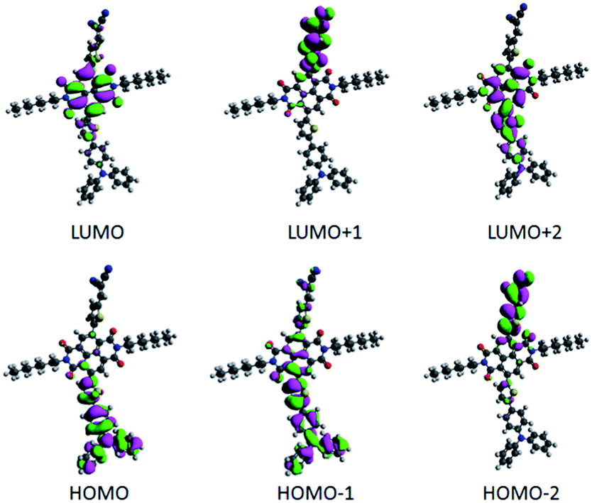 | ||
| Fig. 3 Orbital density distribution for the HOMOs (lower) and LUMOs (upper) of S1. DFT calculations were performed using the Gaussian 09 suite of programs and B3LYP/6-311+G(d,p)//B3LYP/6-31G(d) level of theory. | ||
Experimental estimation of HOMO energies was carried out using photo electron spectroscopy in air (PESA) and the LUMO energies were calculated by adding the band gap to the HOMO values (see Fig. 4 for energy level diagram, and Fig. S2† for PESA curve).
 | ||
| Fig. 4 Energy level diagram depicting the band gaps of S1 and R1 in comparison with P3HT and PC61BM. | ||
The UV-vis spectra indicated that insertion of NDI unit reduces the band gap of S1 when compared with R1. PESA and UV-vis spectra indicated that the band gaps of these materials are all in the range required of donor materials for BHJ devices and are significantly narrower in magnitude than 1.8 eV measured for P3HT. The LUMO of S1 was the lowest of two due to the bathochromic shift observed in the thin film spectrum when compared with R1. The optical and electrochemical properties of both the materials are summarized in Table S1 (see ESI†).
Initial screening into the potency of S1 as a donor material (p-type) was carried out by using it in a solution-processed BHJ device with conventional n-type soluble fullerene derivative PC61BM, and its performance under simulated sunlight and monochromatic light illumination was characterized. BHJ architectures typically deliver higher power conversion efficiencies (PCEs) by maximising the surface area of interface between the p-and n-type materials in the active layer. The blend solution of S1 and PC61BM was used to cast an active layer on top of the PEDOT:PSS surface. The BHJ device architecture used was ITO/PEDOT:PSS (38 nm)/active layer/Ca (20 nm)/Al (100 nm) where the active layer was a solution processed blend of S1 and PC61BM. For S1, a promising PCE of 3.01% was achieved when the film was spin-coated from a chlorobenzene solution as a 1:1 blend with PC61BM. By contrast, the maximum PCE obtained for a device based on R1 was 1.10%, when fabricated under similar conditions. The comparative current–voltage curves for the optimized blends of S1 and R1 with PC61BM are shown in Fig. 5.
 | ||
| Fig. 5 Current–voltage curves for the optimized devices based on S1 and R1 in blends with PC61BM (1:1 wt) under simulated sunlight (AM 1.5, 1000 W m−2). Device structure is: ITO/PEDOT:PSS (38 nm)/active layer/Ca (20 nm)/Al (100 nm) where the active layers were the blends of materials and PC61BM spun on top of the films of PEDOT:PSS using chlorobenzene. | ||
The optimized devices based on S1 showed lower open circuit voltages (Voc) than the devices based on R1. These values are consistent with the measured HOMO values where the more positive HOMO for compound S1 would predict a lower Voc. Devices based on S1 showed higher photocurrent than the devices based on R1, a finding that is consistent with the observed bathochromic-shift in the absorption spectrum of S1 compared with R1. The BHJ devices based on S1 yielded promising performance and the photovoltaic cell parameters, Voc, short circuit current density (Jsc), fill factor (FF) and PCE, reached 0.90 V, 7.90 mA cm−2, 0.43 and 3.01%, respectively. Overall, the insertion of NDI functionality into the studied D–A module resulted in around 80% increase in the photocurrent density and enhanced the PCE by a factor of >2, thus promoting the use of an electron accepting and highly conjugated functionality as an interesting structural concept for the design and development of highly efficient BHJ materials. With regards to the processing conditions of blend solutions, it has been shown4a that there exists a strong relationship between the degree of crystallization and solvent selection on the cell performance. Our attempts to fabricate devices using low boiling solvents, such as CHCl3, resulted in very poor photovoltaic performance. This was primarily due to low film quality. The use of high-boiling solvent is further preferable from a processing point of view.
The incident-photon-to-current conversion efficiency (IPCE) curves of the best BHJ devices based on these small molecules under monochromatic light are shown in Fig. 6. The analysis of the IPCE measurements of these BHJ devices reveals a significantly higher and broader peak IPCE of S1 (∼42% at 640 nm) compared to R1 (38% at 515 nm), which is presumably caused by the synergetic effect of excellent light-harvesting and tuned electrochemical properties. The IPCE measurements reported here are comparable to the film absorptions of S1 and R1 which indicate that the current arises mainly from the p-type donor material. Note that S1 shows light harvesting and electrochemical properties that are largely superior to R1, which translates to higher conversion efficiency.
 | ||
| Fig. 6 Comparative IPCE curves of the best BHJ devices based on S1 and R1. | ||
The active layer morphology was examined by an atomic force microscope (AFM) technique in tapping mode. The actual surface morphology of blend film of S1:PC61BM (1:1, w/w; as cast) is depicted in Fig. 7. The as casted film exhibited crystalline grains with a root-mean-square (RMS) roughness of 0.32 nm. The crystalline grains may be beneficial to ordered structure formation and charge transport in thin film. The hole only mobility in the BHJ blend film was measured by a space-charge limited current (SCLC) method with device structure of ITO/PEDOT:PSS/active layer/Au. A hole mobility of 8.5 × 10⁻⁶ cm2 V−1 s−1 was obtained for the blend of S1 and PC61BM.
 | ||
| Fig. 7 AFM image of 1:1 blend film with PC61BM spin-casted from chlorobenzene at 2500 rpm atop annealed ITO/PEDOT:PSS substrate. Topographic image (as-cast) with RMS 0.32 nm of S1:PC61BM. | ||
Even though the progress in the development of small molecular donors is on surge, the material reported in this paper has highlighted the potential for efficiency improvements in a given D–A system. The discovery of such materials exhibiting promising optoelectronic properties opens up a way to develop such motifs (based on the insertion of highly conjugated, planar functionality) and paves the way for such materials to be used for other organic electronic applications such as organic field-effective transistors.
In conclusion, we have demonstrated the first use of a NDI functionality to improve the optoelectronic and photovoltaic properties of D–A small molecules in organic solar cells. In a direct comparison we have shown that the incorporation of this electron accepting, highly conjugated and planar system lowers the band gap of an oligothiophene dye, S1, and shows higher PCE compared with an analogue, R1. S1 showed excellent thermal stability and solubility in common organic solvents, strong optical absorption over the whole visible region, low lying HOMO energy level and good photovoltaic performance. Based on the optoelectronic characterization and BHJ parameters, it is evident that the design concept addressed herein has huge potential to generate a series of novel organic materials whose properties can be tailored towards their use in conjunction with alternative accepting functionalities. We strongly believe that S1 represents a valuable addition to the library of small molecular electron donors that will form the basis for next generation of custom-designed high-efficiency materials.
Acknowledgements
Sid. V. B. would like to thank the TAPSUN programme for financial assistance under the project NWP0054 and V. Jayathirtha Rao for providing facilities. S.R.B. would like to thank CSIR, New Delhi for SRF fellowship. Sh. V. B. acknowledges Australian Research Council for financial support through a Future Fellowship Scheme (FT110100152). A.G. acknowledges CSIRO and the RMIT University for a visiting fellow position. A.G. acknowledges the assistance of Dr Jegadesan Subbiah (Bio21 Institute, University of Melbourne) for providing support during the fabrication of BHJ devices.Notes and references
- (a) G. Yu, J. Gao, J. C. Hummelen, F. Wudl and A. J. Heeger, Science, 1995, 270, 1789 CAS; (b) G. Li, V. Shrotriya, J. S. Huang, Y. Yao, T. Moriarty, K. Emery and Y. Yang, Nat. Mater., 2005, 4, 864 CrossRef CAS; (c) S. H. Park, A. Roy, S. Beaupre, S. Cho, N. Coates, J. S. Moon, D. Moses, M. Leclerc, K. Lee and A. J. Heeger, Nat. Photonics, 2009, 3, 297 CrossRef CAS; (d) Y. Liang, Z. Xu, J. Xia, S.-T. Tsai, Y. Wu, G. Li, C. Ray and L. Yu, Adv. Mater., 2010, 22, E135 CrossRef CAS PubMed; (e) S. B. Darling and F. You, RSC Adv., 2013, 3, 17633 RSC.
- (a) S. Günes, H. Neugebauer and N. S. Sariciftci, Chem. Rev., 2007, 107, 1324 CrossRef PubMed; (b) B. C. Thompson and J. M. J. Frechet, Angew. Chem., Int. Ed., 2008, 47, 58 CrossRef CAS PubMed; (c) X. Yang and J. Loos, Macromolecules, 2007, 40, 1353 CrossRef CAS; (d) B. Kippelen and J.-L. Brèdas, Energy Environ. Sci., 2009, 2, 251 RSC; (e) Y.-J. Cheng, S.-H. Yang and C.-S. Hsu, Chem. Rev., 2009, 109, 5868 CrossRef CAS PubMed.
- (a) A. Facchetti, Chem. Mater., 2011, 23, 733 CrossRef CAS; (b) H. Patil, W. X. Zu, A. Gupta, V. Chellappan, A. Bilic, P. Sonar, A. Rananaware, S. V. Bhosale and S. V. Bhosale, Phys. Chem. Chem. Phys., 2014, 16, 23837 RSC; (c) A. Gupta, S. E. Watkins, A. D. Scully, T. B. Singh, G. J. Wilson, L. J. Rozanski and R. A. Evans, Synth. Met., 2011, 161, 856 CrossRef CAS PubMed; (d) A. M. Raynor, A. Gupta, H. Patil, A. Bilic and S. V. Bhosale, RSC Adv., 2014, 4, 57635 RSC.
- (a) B. Walker, C. Kim and T.-Q. Nguyen, Chem. Mater., 2011, 23, 470 CrossRef CAS; (b) Y. Li, Q. Guo, Z. Li, J. Pei and W. Tian, Energy Environ. Sci., 2010, 3, 1427 RSC; (c) J. E. Anthony, Chem. Mater., 2011, 23, 583 CrossRef CAS; (d) A. Mishra and P. Bäuerle, Angew. Chem., Int. Ed., 2012, 51, 2020 CrossRef CAS PubMed; (e) Y. Lin, Y. Li and X. Zhan, Chem. Soc. Rev., 2012, 41, 4245 RSC.
- (a) B. C. Thompson and J. M. Frèchet, Angew. Chem., Int. Ed., 2008, 47, 58 CrossRef CAS PubMed; (b) G. Dennler, M. C. Scharber and C. J. Brabec, Adv. Mater., 2009, 21, 1323 CrossRef CAS; (c) J. Chen and Y. Cao, Acc. Chem. Res., 2009, 42, 1709 CrossRef CAS PubMed; (d) Y.-J. Cheng, S.-H. Yang and C.-S. Hsu, Chem. Rev., 2009, 109, 5868 CrossRef CAS PubMed; (e) Y. Li and Y. Zou, Adv. Mater., 2008, 20, 2952 CrossRef CAS.
- (a) Z. Li, G. He, X. Wan, Y. Liu, J. Zhou, G. Long, Y. Zuo, M. Zhang and Y. Chen, Adv. Energy Mater., 2012, 2, 74 CrossRef CAS; (b) T. S. Vander Poll, J. A. Love, T.-Q. Nguyen and G. C. Bazan, Adv. Mater., 2012, 24, 3646 CrossRef CAS PubMed; (c) J. Zhou, X. Wan, Y. Liu, Y. Zuo, Z. Li, G. He, G. Long, W. Ni, C. Li, X. Su and Y. Chen, J. Am. Chem. Soc., 2012, 134, 16345 CrossRef CAS PubMed; (d) V. Gupta, A. K. K. Kyaw, D. H. Wang, S. Chand, G. C. Bazan and A. J. Heeger, Sci. Rep., 2013, 3, 1965 Search PubMed; (e) J. Zhou, Y. Zuo, X. Wan, G. Long, Q. Zhang, W. Ni, Y. Liu, Z. Li, G. He, C. Li, B. Kan, M. Li and Y. Chen, J. Am. Chem. Soc., 2013, 135, 8484 CrossRef CAS PubMed.
- (a) N. M. Kronenberg, M. Deppisch, F. Würthner, H. W. A. Lademann, K. Deing and K. Meerholz, Chem. Commun., 2008, 6489 RSC; (b) N. M. Kronenberg, V. Steinmann, H. Bürckstümmer, J. Hwang, D. Hertel, F. Würthner and K. Meerholz, Adv. Mater., 2010, 22, 4193 CrossRef CAS PubMed; (c) A. B. Tamayo, X.-D. Dang, B. Walker, J. Seo, T. Kent and T.-Q. Nguyen, Appl. Phys. Lett., 2009, 94, 103301 CrossRef PubMed; (d) B. Walker, A. B. Tamayo, X.-D. Dang, P. Zalar, J. H. Seo, A. Garcia, M. Tantiwiwat and T.-Q. Nguyen, Adv. Funct. Mater., 2009, 19, 1 Search PubMed; (e) A. Gupta, A. Ali, A. Bilic, M. Gao, K. Hegedus, B. Singh, S. E. Watkins, G. J. Wilson, U. Bach and R. A. Evans, Chem. Commun., 2012, 48, 1889 RSC; (f) A. Gupta, V. Armel, W. Xiang, G. Fanchini, S. E. Watkins, D. R. MacFarlane, U. Bach and R. A. Evans, Tetrahedron, 2013, 69, 3584 CrossRef CAS PubMed; (g) R. J. Kumar, Q. I. Churches, J. Subbiah, A. Gupta, A. Ali, R. A. Evans and A. B. Holmes, Chem. Commun., 2013, 49, 6552 RSC; (h) A. Gupta, A. Ali, T. B. Singh, A. Bilic, U. Bach and R. A. Evans, Tetrahedron, 2012, 68, 9440 CrossRef CAS PubMed; (i) A. Gupta, A. Ali, A. Bilic, T. B. Singh and R. A. Evans, Dyes Pigm., 2014, 108, 15 CrossRef CAS PubMed.
- (a) S. V. Bhosale, C. Jani and S. Langford, Chem. Soc. Rev., 2008, 37, 331 RSC; (b) H. Patil, A. Gupta, A. Bilic, S. V. Bhosale and S. V. Bhosale, Tetrahedron Lett., 2014, 55, 4430 CrossRef CAS PubMed; (c) H. Patil, A. Gupta, A. Bilic, S. L. Jackson, K. Latham and S. V. Bhosale, J. Electron. Mater., 2014, 43, 3243 CrossRef CAS.
- M. J. Frisch, et al., Gaussian 09 revision D.01, Gaussian Inc., Wallingford CT, 2013 Search PubMed.
Footnotes |
| † Electronic supplementary information (ESI) available: Synthetic procedures, S1 spectra, PESA and TGA curves. See DOI: 10.1039/c4ra13588a |
| ‡ SRB and AG contributed equally to this work. |
| This journal is © The Royal Society of Chemistry 2015 |