
Introducing a protective interlayer of TiO2 in Cu2O–CuO heterojunction thin film as a highly stable visible light photocathode†
Peng Wanga,
Xiaoming Wenb,
Rose Amal*a and
Yun Hau Ng*a
aParticles and Catalysis Research Group, School of Chemical Engineering, The University of New South Wales, Sydney, NSW 2052, Australia. E-mail: yh.ng@unsw.edu.au; r.amal@unsw.edu.au
bSchool of Photovoltaics and Renewable Energy Engineering, The University of New South Wales, Sydney, NSW 2052, Australia
First published on 11th December 2014
Abstract
Visible light-induced photocurrent generation and photoelectrochemical stability of p-type Cu2O–CuO photocathodes are improved significantly upon incorporating an interlayer of TiO2 between Cu2O and CuO. The TiO2 layer hinders the electron conduction at the semiconductor–electrolyte interface (improved stability) as well as promoting electron transfer from Cu2O to CuO (increased photocurrent). Upon visible light illumination, the optimised multilayer Cu2O–TiO2–CuO heterojunction thin film yields a photocurrent of 2.4 mA cm−2 and retains 75% of its photoactivity over the measurement period. By comparison, the unmodified Cu2O–CuO generates a photocurrent of 1.3 mA cm−2 with photoactivity retention of only 32% after prolonged illumination. Wavelength-dependent incident photon-to-current efficiency (IPCE) reveals a considerable enhancement over the excitation region of Cu2O (400–560 nm). Transient fluorescence decay analysis suggests the promotion of electron transfer from Cu2O to CuO through TiO2. As a result, both photoactivity and photochemical stability of the photocathodes are improved.
Introduction
Splitting water into its elemental components, i.e. H2 and O2, is regarded as the cleanest and the most sustainable way to meet energy demands while addressing stringent environmental concerns. Even though traditional electrolysis of water has been known for decades,1 currently water splitting triggered by sunlight is attracting the attention of the research community as energy input, conversion and output all occur in clean and renewable forms.2 Since the discovery of photoelectrochemical (PEC) water splitting using UV-illumined TiO2 electrodes by Honda and Fujishima,3 extensive work has been carried out to develop an efficient PEC water splitting system. Various photoactive electrodes have been made and investigated with the majority of the examples based on n-type semiconductors (e.g. WO3,4 BiVO4 (ref. 5) and GaInP2 (ref. 6)). Electrons photogenerated in n-type semiconductors, with the aide of external voltage supplied, can be transported to the counter electrode (mostly platinum (Pt)) to reduce water. A p-type photoactive semiconductor is the ideal candidate to replace Pt for use in a “tandem” configuration which excludes or minimises the supply of external energy to split water in a photoelectrochemical process.7,8 However, few examples of highly efficient p-type semiconductors have been reported so far.p-type Cu2O has distinguished itself by its abundance, low-cost and, more impressively, its high theoretical photocurrent of −14.7 mA cm−2.9–11 It has a suitable direct optical band gap of 2–2.2 eV (λ < 560 nm in the visible light range), where the conduction band (CB) is 0.7 V more negative than the reduction potential of water and the valence band (VB) is just more positive than the oxidation potential of water.9,10 Electrons excited into CB of Cu2O are sufficiently energetic to be transferred to water for H2 production. Despite all these advantages, the Cu2O photoelectrode is chemically unstable due to a self-photodegradation mechanism. As the redox potential of Cu2O lies between its CB and VB, it can either be self-reduced (Cu2O to Cu) or self-oxidised (Cu2O to CuO) by the photogenerated electrons or holes, respectively, upon visible light illumination.12 Thimsen and co-workers introduced an ultra-thin protective layer of ZnO:Al/TiO2 on top of the Cu2O photoelectrode using atomic layer deposition (ALD).12 The ZnO:Al/TiO2 layer protected Cu2O from direct electron conduction with the electrolyte interface. Instead, it allowed the electrons to flow from Cu2O to the electrolyte through the protective layer. This strategy greatly suppressed the photodegradation of Cu2O. It has been adopted for surface passivation of other p-type photocathodes including Si-photoelectrode to extend the lifetime of p-type semiconductors in a solid–liquid junction cell.13,14 Nonetheless, ALD treatment of thin film requires costly instrumentation and large-scale treatment is challenging. Wang's group subsequently introduced a thin CuO layer with a function similar to the previously elaborated ZnO:Al/TiO2 on Cu2O photoelectrode by using a combination of electrodeposition, anodisation and calcination.15 The CuO top layer was found to reduce the photocorrosion of Cu2O as well as the charge recombination rate during water splitting reaction.
We recently developed an anodised Cu2O thin film with the surface decorated with CuO nanowires grown from the Cu2O layer underneath.16 The embedment of these CuO nanowires derived from thermal treatment was found to improve the adhesion of Cu2O layers to the substrate. The enhanced mechanical stability together with the partial surface passivation towards the Cu2O–electrolyte interface contributed to an improved PEC stability of the film. In this work, adopting the working principle of surface passivation, by using a dip-coating technique we introduce an interlayer of anatase TiO2 in between the Cu2O under layer and CuO top layer. Dip-coating is a fast, simple and, more importantly, scalable method of large film treatment. The introduction of TiO2 interlayer offers a number of advantages to improve the PEC performance of the Cu2O photocathode. Firstly, it minimises the direct electron conduction between Cu2O and electrolyte, which usually leads to the photocorrosion of Cu2O. Secondly, a thin layer of TiO2 does not affect the penetration of visible light to reach Cu2O underneath; therefore, comparable light absorption in Cu2O could be expected. Thirdly, the strategic alignment of the band gap structure among Cu2O, TiO2 and CuO can promote an efficient electron transfer pathway for higher electron consumption efficiency. As a result, both photocurrent generation and retention of photoactivity in our new photoelectrodes were greatly improved. A thorough investigation on the origin of the enhancement was performed and the electron transfer kinetics between the tri-components was studied.
Experimental section
Preparation of unmodified and TiO2-modified Cu2O–CuO photoelectrodes
All chemicals used in these studies were of analytical grade without further purification. The Cu foil (99.9%, Aldrich) was sonicated first in ethanol–acetone solution (1![[thin space (1/6-em)]](https://www.rsc.org/images/entities/char_2009.gif) :1), followed by Milli-Q water for 10 min each. A two-electrode, in-house designed anodisation cell was used, with Cu foil as the working electrode and platinum plate and wire as the counter electrode. Cu2O was synthesised by anodising the Cu foil in an alkaline electrolyte at 10 V for 10 min by a programmable DC power supply (PST-3201, GW Instek). The alkaline electrolyte was composed of 96.05 wt% of ethylene glycol (>99%, Aldrich), 0.75 wt% of potassium hydroxide (>99%, Aldrich) and 3.0 wt% of water with 0.20 wt% sodium fluoride (>99%, Aldrich). After anodisation, the prepared Cu2O foil was washed with Milli-Q water to remove unwanted debris or precipitates and dried under ambient air for 1 h. The unmodified Cu2O–CuO photoelectrode was fabricated by calcination of the anodised Cu2O thin film at 400 °C for 1 h. The TiO2-modified Cu2O–CuO photoelectrode was synthesised by dip-coating to create a TiO2 interlayer between the Cu2O under layer and CuO top layer. A pre-determined optimised 2.0 M titanium isopropoxide solution in ethanol was used as the TiO2 precursor. The dip-coating procedure on the anodised Cu2O foil was carried out for 30 min. In order to investigate the influence of TiO2 coverage on Cu2O–CuO photoelectrodes, Cu2O–CuO photoelectrodes modified with 2.0 M TiO2 precursor at different duration ranging from 10 min to 60 min were also prepared. After dip-coating of TiO2 precursor, the foils were annealed in air at identical conditions.
:1), followed by Milli-Q water for 10 min each. A two-electrode, in-house designed anodisation cell was used, with Cu foil as the working electrode and platinum plate and wire as the counter electrode. Cu2O was synthesised by anodising the Cu foil in an alkaline electrolyte at 10 V for 10 min by a programmable DC power supply (PST-3201, GW Instek). The alkaline electrolyte was composed of 96.05 wt% of ethylene glycol (>99%, Aldrich), 0.75 wt% of potassium hydroxide (>99%, Aldrich) and 3.0 wt% of water with 0.20 wt% sodium fluoride (>99%, Aldrich). After anodisation, the prepared Cu2O foil was washed with Milli-Q water to remove unwanted debris or precipitates and dried under ambient air for 1 h. The unmodified Cu2O–CuO photoelectrode was fabricated by calcination of the anodised Cu2O thin film at 400 °C for 1 h. The TiO2-modified Cu2O–CuO photoelectrode was synthesised by dip-coating to create a TiO2 interlayer between the Cu2O under layer and CuO top layer. A pre-determined optimised 2.0 M titanium isopropoxide solution in ethanol was used as the TiO2 precursor. The dip-coating procedure on the anodised Cu2O foil was carried out for 30 min. In order to investigate the influence of TiO2 coverage on Cu2O–CuO photoelectrodes, Cu2O–CuO photoelectrodes modified with 2.0 M TiO2 precursor at different duration ranging from 10 min to 60 min were also prepared. After dip-coating of TiO2 precursor, the foils were annealed in air at identical conditions.
Material characterization
The morphology and nanostructure of unmodified Cu2O–CuO and TiO2-modified Cu2O–CuO photoelectrodes were analysed by scanning electron microscopy (SEM, S900, Hitachi). The phase and crystallinity of the thin film were investigated by X-ray diffraction (XRD, X'pert Pro MRD, Philips, using Cu Kα radiation λ = 1.54 Å). The distribution of TiO2 particles on the layer of Cu2O was detected by energy dispersive spectrometry (EDS, NanoSEM 230, FEI Nova). The surface chemical composition was characterized by X-ray photoemission spectrometry (XPS, ESCALAB220i-XL, Thermo Scientific) with Al Kα at 1486.6 eV. All the XPS data were calibrated to the carbon 1s peak at 285 eV. Fluorescence lifetimes were measured using the time correlated single photon counting (TCSPC) technique on a Microtime-200 system (Picoquant) with an excitation by a 405 nm laser. The system has time resolution of about 200 ps.Photoelectrochemical performance
Photoelectrochemical characterization was carried out using a standard three-electrode electrochemical cell, which has a quartz window for light penetration and a hole for clamping samples. Platinum wire was used as the counter electrode and an Ag/AgCl electrode was employed as the reference electrode. The electrolyte used for all PEC measurements was a 0.5 M K2SO4 solution purged with argon to remove dissolved air. The photoelectrochemical properties including photocurrent density and photocurrent transient responses were recorded with a potentiostat (PG STAT-302N, Autolab) under on–off illumination cycles. The illumination source was a 300 W xenon arc lamp (PLS-SXE300) equipped with cut-off filter at 420 nm. Incident photon-to-current efficiency (IPCE) was measured using a 280 W xenon lamp (Newport 66902) coupled with a monochromator (Newport 74125).Results and discussion
Fig. 1a and b show the surface morphology of unmodified Cu2O–CuO and TiO2-modified Cu2O–CuO photoelectrodes. As described in our earlier work using high resolution transmission electron microscopy,16 the unmodified Cu2O–CuO photoelectrode comprises two distinct component layers, i.e. a compact under layer of Cu2O and a densely packed top layer of CuO nanowires. The growth of CuO nanowires from the bottom of the Cu2O layer was found to be initiated by thermal treatment.17 After modification with TiO2, a relatively lower concentration of surface CuO nanowires was observed while the formation of interconnected TiO2 particles was detected underneath these CuO nanowires. The X-ray diffraction patterns of unmodified Cu2O–CuO and TiO2-modified Cu2O–CuO photoelectrodes were compared in Fig. 1c. In addition to the peaks assigned to crystalline Cu2O (36.4° and 42.3°) and CuO (38.7°), a small peak at 25.2° attributed to anatase TiO2 was observed in the TiO2-modified thin film. The Rietveld analysis revealed that the predominant component was Cu2O (∼50%) followed by a small amount of CuO (∼15%) and TiO2 (∼4%), and the rest was attributed to the Cu substrate.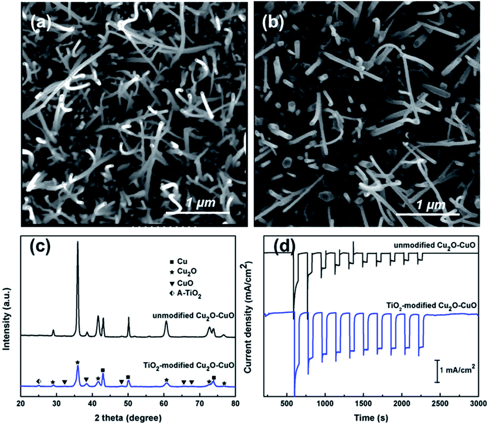 | ||
| Fig. 1 SEM images of (a) unmodified Cu2O–CuO and (b) TiO2-modified Cu2O–CuO photoelectrodes; (c) XRD patterns and (d) visible light (>420 nm) photocurrent generation of unmodified Cu2O–CuO and TiO2-modified Cu2O–CuO photoelectrodes. | ||
Fig. 1d shows the photocurrent generation using unmodified Cu2O–CuO and TiO2-modified Cu2O–CuO photoelectrodes at −0.36 V vs. Ag/AgCl under visible light illumination (>420 nm). When Cu2O semiconductor was exposed to visible light illumination with energy greater than its band gap, electrons and holes were generated within the semiconductor. Under a negative bias against a Pt counter electrode, electrons were flown from the Pt counter electrode to the Cu2O working electrode generating a cathodic current. The observed photocathodic current confirmed the p-type behaviour of the Cu2O electrode.18 The unmodified Cu2O–CuO photoelectrode generated an initial photocurrent density of 1.3 mA cm−2 but experienced a severe photocurrent decay upon repeating the on–off illumination cycles indicating its photocorrosion, which represents a common issue in Cu2O-based electrodes. Upon modification with TiO2, the initial photocurrent density reached 2.4 mA cm−2 (which is an 85% photocurrent enhancement). More importantly, the photocurrent profile underwent only a mild decay over the measurement period, with 75% of the initial photocurrent density being retained. With the protective layer of TiO2 presenting above the Cu2O surface, the Cu2O–electrolyte interaction was limited to minimise the problematic direct electron conduction. Additionally, the transfer of photogenerated electrons from Cu2O to TiO2 was thermodynamically favoured as the CB of Cu2O is more negative than that of TiO2.19 Combining the reduced rate of photocorrosion and the improved charge transfer mechanism, the PEC performance of TiO2-modified photoelectrodes was higher and more stable. A similar trend, i.e. increased photocurrent generation and improved photocurrent stability, was also observed when the Cu2O–CuO photoelectrodes were modified with different concentrations of the TiO2 precursor indicating a constructive effect of having a thin TiO2 protecting layer (please refer to Fig. S1 in ESI†). Another noticeable aspect of the measurements is that the anatase TiO2 (band gap of 3.2 eV) remained at its ground state without being photoexcited in visible light. Thus, TiO2 did not contribute an extra electron pool in the photocurrent generation but provided an efficient platform for electron transfer.
As the coverage of TiO2 on the Cu2O surface is presumably critical in preventing direct contact with the electrolyte as well as facilitating efficient electron transfer pathways, an investigation on the TiO2 coating patterns was performed. Fig. 2 shows the SEM images of Cu2O–CuO photoelectrodes modified with precursor of TiO2 at different duration. At a short coating time of 10 min, apparent agglomeration of small particles was observed with the CuO nanowires penetrating the surface from the Cu2O layer underneath. The growth of the agglomerates continued as a longer coating time was applied. For a 60 min photoelectrode coating time, a development of clear grain boundaries (defined as “cracks” between agglomerates) was evident. The grain boundaries significantly influenced the electron transport by introducing defects or charge trap sites for electron–hole recombination, which impeded the shuttling of electrons. In addition, the “cracks” between agglomerates allowed diffusion of the electrolyte to reach the under layer of Cu2O, thus diminishing the “protective” role of TiO2. Elemental mappings of the photoelectrodes over a larger area are presented in Fig. 3, where the identity of agglomerates observed in Fig. 2 is verified as TiO2 (supported by XRD in Fig. 1c). Although at a microscopic level (1 μm scale) the TiO2 agglomerates appeared to be evenly coated over Cu2O, the overall coverage of TiO2 was relatively poor (10 μm scale) as can be seen in the elemental map in Fig. 3a. In contrast, photoelectrodes coated for both 30 min and 60 min showed comparable and considerable TiO2 coverage on the surface of Cu2O. The thickness of the 30 min-coated TiO2 was estimated by back scattered electrons (BSE) imaging to be ca. 140 nm (Fig. S2 in ESI†). The main photoelectrochemical differences between the 30 min and 60 min coating procedures stemmed from the difference in the produced morphological features; photoelectrodes modified for 60 min presented formation of much more severe grain boundaries, which resulted in decreased photocurrent and stability, as will be elaborated below.
 | ||
| Fig. 2 SEM images of Cu2O–CuO photoelectrodes modified with precursor of TiO2 at different duration: (a) 10 min; (b) 30 min; (c) 60 min. | ||
 | ||
| Fig. 3 Energy dispersive X-ray spectroscopy mapping images of Cu2O–CuO photoelectrodes modified with precursor of TiO2 at different duration. (a) 10 min; (b) 30 min; (c) 60 min. | ||
As shown in Fig. 4, the coating process influences the photocurrent generation and the photoelectrochemical stability of TiO2-modified Cu2O–CuO photoelectrodes. In general, our measurements for Cu2O–CuO photoelectrodes modified with an interlayer of TiO2 revealed two main findings: (1) an increase in the magnitude of the cathodic photocurrent generation, and (b) a slower photocurrent decay over time reflecting the improved stability. As indicated in Fig. 4a, all TiO2-modified photoelectrodes demonstrated higher initial photocurrent density upon visible light illumination than that of the unmodified Cu2O–CuO photoelectrode. The initial photocurrent densities were 1.3, 1.6, 2.4 and 1.5 mA cm−2 for unmodified, 10, 30, and 60 min-modified Cu2O–CuO photoelectrodes, respectively. Photoelectrochemical stability towards self-photodegradation was estimated by monitoring the photocurrent decay over the measurement period (Fig. 4b).20 The photoelectrodes prone to the most severe photocorrosion demonstrated the fastest photocurrent decay resulting in low photoactivity at the end of the measurement. The Cu2O–CuO photoelectrode modified with TiO2 for 30 min showed the highest photocurrent generation and retained 75% of its initial photoactivity over 40 min of measurement. Even though they performed better than unmodified Cu2O–CuO photoelectrode, the photoelectrodes modified for 10 and 60 min, were inferior in both aspects. As the conduction band of TiO2 lies lower than that of Cu2O, the presence of a TiO2 layer on top of Cu2O created a thermodynamically feasible pathway to shuttle the electrons photogenerated in Cu2O. The creation of a junction between TiO2 and CuO facilitates charge transfer, thus improving the overall photocurrent generation. In accordance with the TiO2 coverage and agglomeration states shown in Fig. 2 and 3, the Cu2O–CuO photoelectrode modified with TiO2 for 30 min revealed the most optimal TiO2 coverage with small dispersed aggregates that provided the most “protective” and surface passivating function for Cu2O. Samples with low coverage (modified for 10 min) and a large amount of cracks between large agglomerates (modified for 60 min) showed relatively ineffective surface passivation. They only retained 65% (modified for 10 min) and 56% (modified for 60 min) of their initial activity, respectively. Another possible reason for lower photoactivity and stability observed in Cu2O–CuO photoelectrode modified for 60 min is the trapping of electrons in the long lived Ti3+ states (please refer to XPS data in Fig. S2 in ESI†).12,21,22 Upon generation in Cu2O, the electrons are efficiently transferred to TiO2. Instead of further injection into CuO or electrolyte, the electrons are possibly reducing Ti4+ to Ti3+ resulting in lower photoactivity.
 | ||
| Fig. 4 (a) Visible light (>420 nm) photocurrent generation and (b) corresponding current decay of Cu2O–CuO photoelectrodes unmodified and modified with precursor of TiO2 at different duration. | ||
Wavelength-dependent photocurrent analysis was performed to measure the incident photon-to-current efficiency of the Cu2O–CuO photoelectrodes (Fig. 5a). As expected, the overall conversion efficiency was higher in TiO2-modified Cu2O–CuO photoelectrodes. Interestingly, the photocurrent enhancement in TiO2-modified Cu2O–CuO photoelectrodes was only observed at the wavelengths shorter than 560 nm, which corresponds to the optical band gap of Cu2O (∼2.2 eV). This result supports the earlier suggestion on the charge transfer from the conduction band of Cu2O to TiO2. As charge recombination is suppressed, higher utilisation rate of electrons is achieved in the wavelength region where Cu2O is excited. The photoactivity in wavelengths longer than 560 nm appeared as the tailing off in the overall photocurrent profile and likely originated from the narrower band gap CuO component in the photoelectrode. Since the electron transfer from CuO to TiO2 is prohibited as the conduction band of CuO is more positive than that of TiO2,23 the presence of TiO2 does not influence the conversion efficiency in this wavelength region. CuO nanowires offer an energetically favourable electron transfer pathway for the electrons originated from Cu2O and TiO2.
 | ||
| Fig. 5 (a) Wavelength-dependent IPCE of unmodified Cu2O–CuO and TiO2-modified Cu2O–CuO photoelectrodes; (b) transient decay curves of commercial Cu2O, unmodified Cu2O–CuO and TiO2-modified Cu2O–CuO photoelectrodes. | ||
Fluorescence lifetimes of commercial Cu2O, unmodified Cu2O–CuO and TiO2-modified Cu2O–CuO photoelectrodes were measured using the time-correlated single photon counting technique (Fig. 5b). Samples were excited at 405 nm and monitored at 510 nm. The decay constants were determined using bi-exponential analysis as shown in eqn (1), from which average lifetimes were obtained using eqn (2).
|
y = A1exp(−t/τ1) + A2exp(−t/τ2)
| (1) |
| 〈τ〉 = (A1τ1 + A2τ2)/(A1 + A2) | (2) |
Conclusions
In summary, we have demonstrated a beneficial impact of coating a thin layer of TiO2 on an anodised Cu2O photoelectrode on its visible light photoelectrochemical performance. Two noticeable improvements were observed: enhanced magnitude of the photocurrent generation and improved photoelectrochemical stability of Cu2O. The increased stability is especially significant as self-photodegradation of Cu2O has been the most challenging aspect of this unstable p-type material for years. Fig. 6 illustrates the schematic configuration of the TiO2-modified Cu2O–CuO photoelectrode prepared in this work. Based on the experimental results obtained, the photoelectrochemical properties are proposed to be enhanced through: (1) Cu2O surface passivation by TiO2, preventing redox reactions at the Cu2O–electrolyte interface; and (2) improved charge transport channels attributed to the well-aligned band gap structure, in which the photoexcited electrons in Cu2O are thermodynamically transferred to TiO2 or CuO nanowires or from Cu2O to TiO2 and subsequently CuO nanowires. The embedment of one-dimensional CuO nanowires underneath the Cu2O layer also improved the physical stability of the well-designed Cu2O–TiO2–CuO heterojunction thin film. Instead of the electron transfer by random diffusion from Cu2O to the interface, the embedment of one-dimensional CuO nanowires provided a fast and direct electron transfer pathway. Although a complete inhibition of the photoactivity decay was not achieved at this stage, this work opens immense possibilities for improvement by further optimisation of the process. | ||
| Fig. 6 Schematic illustration of (a) TiO2-modified Cu2O–CuO photoelectrodes; (b) corresponding energy band positions; electron diffuse transfer from Cu2O to interface (c) without one-dimensional CuO nanowires and (d) with one-dimensional CuO nanowires. | ||
Author contributions
P. W. fabricated the photoelectrodes, conducted SEM, EDS, XRD, PEC and IPCE measurements. Dr B. G. conducted XPS experiment and analysis. Dr X. M. W. conducted TCSPC measurement and analysed data. Prof. R. A. and Dr Y. H. N. supervised this work. All authors analysed the data and completed the paper.Acknowledgements
This work was financially supported by the Australia Research Council Discovery Project (DP 110101638). The authors would like to acknowledge the UNSW Mark Wainwright Analytical Centre for providing facility and technical supports. Dr Bill Gong from Solid State & Elemental Analysis Unit of UNSW is gratefully acknowledged for his help in XPS measurement and analysis. The authors thank Carlos G. Morales-Guio and Prof. Xile Hu from École Polytechnique Fédérale de Lausanne (EPFL) for assistance in the back scattered electron (BSE) imaging.Notes and references
- S. Trasatti, J. Electroanal. Chem., 1999, 476, 90–91 CrossRef CAS.
- R. Abe, J. Photochem. Photobiol., C, 2010, 11, 179–209 CrossRef CAS PubMed.
- A. Fujishima and K. Honda, Nature, 1972, 238, 37–38 CrossRef CAS.
- C. Ng, A. Iwase, Y. H. Ng and R. Amal, ChemSusChem, 2013, 6, 291–298 CrossRef CAS PubMed.
- Y. H. Ng, A. Iwase, A. Kudo and R. Amal, J. Phys. Chem. Lett., 2010, 1, 2607–2612 CrossRef CAS.
- O. Khaselev and J. A. Turner, J. Electrochem. Soc., 1998, 145, 3335–3339 CrossRef CAS PubMed.
- C. G. Morales-Guio, S. D. Tilley, H. Vrubel, M. Grätzel and X. Hu, Nat. Commun., 2014, 5, 3059 Search PubMed.
- L. J. Minggu, W. R. Wan Daud and M. B. Kassim, Int. J. Hydrogen Energy, 2010, 35, 5233–5244 CrossRef CAS PubMed.
- A. J. Nozik and R. Memming, J. Phys. Chem., 1996, 100, 13061–13078 CrossRef CAS.
- A. J. Nozik, Appl. Phys. Lett., 1977, 30, 567–569 CrossRef CAS PubMed.
- Y. Li and J. Zhang, Laser Photonics Rev., 2010, 4, 517–528 CrossRef CAS.
- A. Paracchino, V. Laporte, K. Sivula, M. Grätzel and E. Thimsen, Nat. Mater., 2011, 10, 456–461 CrossRef CAS PubMed.
- K. Sun, N. Park, Z. Sun, J. Zhou, J. Wang, X. Pang, S. Shen, S. Y. Noh, Y. Jing, S. Jin, P. K. L. Yu and D. Wang, Energy Environ. Sci., 2012, 5, 7872–7877 CAS.
- Y. V. Pleskov, A. M. Kraitsberg, G. Y. Kolbasov, N. I. Taranenko and V. G. Lipyavka, Sol. Energy Mater., 1991, 22, 119–126 CrossRef CAS.
- Z. Zhang and P. Wang, J. Mater. Chem., 2012, 22, 2456–2464 RSC.
- P. Wang, Y. H. Ng and R. Amal, Nanoscale, 2013, 5, 2952–2958 RSC.
- S. L. Shinde and K. K. Nanda, RSC Adv., 2012, 2, 3647–3650 RSC.
- P. E. de Jongh, D. Vanmaekelbergh and J. J. Kelly, J. Electrochem. Soc., 2000, 147, 486–489 CrossRef CAS PubMed.
- W. Siripala, A. Ivanovskaya, T. F. Jaramillo, S. H. Baeck and E. W. McFarland, Sol. Energy Mater. Sol. Cells, 2003, 77, 229–237 CrossRef CAS.
- N. J. Bell, Y. H. Ng, A. Du, H. Coster, S. C. Smith and R. Amal, J. Phys. Chem. C, 2011, 115, 6004–6009 CAS.
- J. P. Yasomanee and J. Bandara, Sol. Energy Mater. Sol. Cells, 2008, 92, 348–352 CrossRef CAS PubMed.
- L. B. Xiong, J. L. Li, B. Yang and Y. Yu, J. Nanomater., 2012, 2012 Search PubMed.
- J. Bandara, C. P. K. Udawatta and C. S. K. Rajapakse, Photochem. Photobiol. Sci., 2005, 4, 857–861 CAS.
Footnote |
| † Electronic supplementary information (ESI) available. See DOI: 10.1039/c4ra13464h |
| This journal is © The Royal Society of Chemistry 2015 |