
Synthesizing graphenes directly on SiO2/Si in open environments by a dual flame method
Wang Gangab,
Zhao Yunbc,
Deng Yaab,
Chen Minjiangab,
Tao Liab,
Fan Xiaokuna,
Huang Wenbina,
Yang Huaichaoab and
Sun Lianfeng*a
aNational Center for Nanoscience and Technology, Chinese Academy of Sciences, Beijing 100190, People's Republic of China. E-mail: slf@nanoctr.cn
bUniversity of Chinese Academy of Sciences, Chinese Academy of Sciences, Beijing 100039, People's Republic of China
cSemiconductor Lighting Technology Research and Development Center, Institute of Semiconductors, Chinese Academy of Sciences, Beijing 100083, People's Republic of China
First published on 27th January 2015
Abstract
In this work, a simple, productive and low cost method is reported for synthesizing few-layer graphenes directly on SiO2/Si substrates. Films of nickel with different thicknesses (25–700 nm) are thermally deposited on SiO2/Si substrates as catalyst. The substrates with nickel films are treated by lighting cotton and alcohol blast burners in sequence and then cooling down quickly. The dual flames last only several minutes. After growth, few-layer graphenes can be found on the upper surface of nickel and at the interfaces between the nickel and the SiO2/Si, which are confirmed by Raman spectroscopy. Few-layer graphenes can be directly obtained on the SiO2/Si substrate after etching off nickel, without further transfer process. Scanning Raman mapping and transmission electron microscopy indicate that the graphenes are uniform, continuous and of high quality. The dependence of the quality of graphenes on the thickness of nickel have been studied and discussed.
1. Introduction
Graphene is a hexagonal arrangement of carbon atoms,1 which form a one atom thick planar sheet.2 Due to its outstanding physical properties, such as high mobility3,4 and thermal conductivity,5 graphene is usually considered as a competitive candidate for electronic devices and accordingly it captures significant attention for both fundamental research and applications. Generally, the main methods to produce graphene include mechanical exfoliation 1, chemical exfoliation of graphite,6,7 chemical vapor deposition (CVD),8–12 thermal decomposition of SiC13 and unzipping carbon nanotubes14,15 etc. Among these, chemical exfoliation and CVD are most promising candidates for large-scale produce of graphene. However, these regular synthesis approaches are always either inefficient or complex for craftwork. In recent years, the flame synthesis method has emerged as a promising technique to produce graphene, due to its merits of simplicity, speed and high efficiency.16–20 Flame synthesis, as its name indicates, generally introduces the flame of a blast burner or alcohol lamp as heat source to synthesize graphene. The flame synthesis method can be easily operated in open environments with facile tools. Nevertheless, as flame synthesis usually uses metal or minerals as substrate to grow graphene,16–20 it cannot be ignored that these synthesis approaches always need transfer processes, which would inevitably introduce contaminants and defects.In this paper, we report a dual flame method to directly grow graphene on dielectric substrates which need no transfer procedure. This method is not only facile but also time and energy saving, which could produce high quality and large scale graphene films in open environments at atmosphere pressure. Here, we successfully synthesize few-layer graphenes directly on SiO2/Si in atmospheric environment by dual flame method. The whole process of our dual flame method to synthesize graphene costs only several minutes. Unlike conventional CVD method, the rapid heating/cooling process and inexistence of hydrocarbon and carrier gas also avoid energy wasting.
2. Experiment
Fig. 1 illustrates the schematic process to directly synthesize transfer-free graphenes on SiO2/Si substrates by dual flame method. As shown in the picture, the cotton is called burner 1 and the alcohol blast burner is called burner 2. First of all, the nickel films were evaporated on SiO2/Si substrates with different thickness (typically 400 nm) by thermal evaporation. Then, we encircled the Ni/SiO2/Si sample by cotton and immerged it into ethanol until the cotton was fully soaked with ethanol. After having done all these preparations, the Ni/SiO2/Si substrate which was surrounded by cotton was burnt in the internal flame of burner 1 by lighting for 20 seconds. In this procedure, carbon source from burner 1 diffused to the nickel films. At last, the Ni/SiO2/Si substrates were heated to 950 centigrade for 50 or 60 s in the outer flame of burner 2, which was called carburization process. The carbon source diffused into the entire nickel film in this process.18,19 After carburization, the burner 2 was switched off and the burner 1 was capped off by a beaker immediately. Because short of oxygen, flame was rapidly extinguished and the Ni/SiO2/Si substrate cooled down to room temperature in the beaker quickly as well. During the cooling down process, carbon solubility in the nickel film decreased dramatically and carbon atoms segregated out from the interior of nickel to the surface in the form of few-layer graphene. Afterward, an etchant solution (CuSiO4![[thin space (1/6-em)]](https://www.rsc.org/images/entities/char_2009.gif) :H2O:HCl = 10 g:50 ml:50 ml) was used to etch away the nickel and then continuous graphenes could be obtained directly on SiO2/Si substrate.
:H2O:HCl = 10 g:50 ml:50 ml) was used to etch away the nickel and then continuous graphenes could be obtained directly on SiO2/Si substrate.
 | ||
| Fig. 1 Schematic procedures of the flame synthesis of graphenes: (1) evaporation of nickel film (typical 400 nm); (2) immerging the sample into ethanol after surrounding the Ni/SiO2/Si substrate by cotton, then lighting it with fire and lasting 20 seconds; (3) burning the sample in outer flame of Burner 2 (alcohol blast burner) for 50–60 seconds; (4) putting out the fire with a beaker; (5) graphene formed after growth and etching off the nickel. | ||
The dual flame from two burners, as shown in the Fig. 1, served as different functions during growth. The flame from burner 1 surrounded the Ni/SiO2/Si substrate during the whole duration of graphene synthesis, protecting the Ni film and graphene from air oxidation and serving as carbon source for graphene segregation. The flame from burner 2 served as heating source of carbonization and provided carbon for graphene growth as well.
The few-layer graphene were confirmed and analysed by Raman spectra (Renishawin via plus) using a 100× objective around 0.4 mW at room temperature.21,22 A DM4000M Leica microscope and a Tecnai F20 TEM (Transmission Electron Microscopy) was used for morphology characterization of obtained graphene.
3. Results and discussion
Our dual flame method to directly grow graphene on SiO2/Si substrates was based on non-equilibrium surface segregation process and carburization/decarburization mechanism,19 which was similar to the CVD method. Carbon solubility in nickel was strongly relevant to temperature. Carbon atoms diffused in the nickel film during the carburization process, and then segregated onto the nickel film surface because of the sharp decrease of carbon solubility in nickel during the cooling down. When synthesizing graphenes on copper, the growth mechanism is attributed to equilibrium segregation process.8 However, if nickel is used as the catalyst to grow graphenes, the growth mechanism is attributed to non-equilibrium segregation process.23,24 The growth mechanism of dual flame in this manuscript is similar to that of growth of graphene by Ni catalyzing at ambient pressure by chemical vapor deposition.23,24 During the growth, graphene segregation occurs while cooling down, which is non-equilibrium process. This mechanism is also discussed and reported in previous works using flame method to grow graphenes.18,193.1 Few-layer graphenes on different kinds of surfaces
After growth, defected graphenes/carbon film could be obtained on top surface of nickel, which is consistent with previous reports.25,26 In fact, during flame synthesis process, the edge of nickel film could occasionally curl up because of uneven heating. We also characterized the lower surface of nickel film that originally attached to SiO2 but curled after growth. We also found that the signals of graphene were detected on the lower surface of nickel, which implied that during the growth process, graphene layers would form at the interface of nickel and SiO2 and attach to nickel or SiO2 depending on its adhesion. Hence, counting in the graphenes on SiO2 substrate after etching away nickel, we found the graphene segregated onto three faces. The nickel films recrystallized in the heating process,27,28 and meanwhile the carbon atoms dissolve into nickel films and then converge at the nickel's grain boundary. As is shown in Fig. 2a, graphenes can be found on different surfaces, including upper surface of nickel, the lower surface of nickel that curl up and the silicon substrate. | ||
| Fig. 2 (a) After growth, graphenes can be found on three surfaces: on the upper side of nickel film (A), on the lower side of curled nickel film (B), on the surface of SiO2 (C). (b) The typical Raman spectra of graphenes from three surfaces which are marked in (a). | ||
Fig. 2b illustrates the typical Raman spectra of graphenes on these three surfaces. It needs to note that three typical Raman spectra are characterized under same experimental methods and conditions. As shown in the picture, high intensity of D peak in black line demonstrates that graphenes on the surface of nickel film (air/nickel) contain lots of defects.21 The ratio of IG/I2D is about 2 which indicates graphenes are few layers. Similarly, according to the weak signal and wide G and 2D peaks, graphenes on the other side of nickel film (nickel/SiO2), Raman spectrum of which is shown as red line in Fig. 2b, are defected as well. It may be the reason of low quality of graphenes on the lower side of nickel that carbon atoms segregate onto the SiO2 surfaces mostly but left little on the nickel/SiO2 surface. In contrast, typical Raman spectra of graphenes on SiO2substrates have tiny D peak and sharp G and 2D peaks, which suggests that graphenes on this surface have much higher degree of crystallization. Peak positions of G bond and 2D bond of each three typical Raman spectra are marked in Fig. 2b. The positions of G and 2D peaks of graphene on Ni have up-shift comparing with that of graphene on silicon substrate, which can be attributed to the substrate effect.29
3.2 Few-layer graphenes on silicon substrates
Fig. 3a is a typical optical image of the graphenes on the SiO2/Si surface after nickel films were etched away by an etchant solution. From the optical image, we can see the continuity and uniformity of graphenes on SiO2/Si substrates obtained by our experiment. In order to get detailed information of graphenes' quality, Raman mapping was used for further characterization. The inset red rectangular in Fig. 3a marks the area of Raman mapping, which show graphenes' IG and ratio of IG/I2D over hundreds of micrometer square area in Fig. 3b and c, respectively. G peaks of graphene obtained by our dual flame method, as illustrated in Fig. 3b, generally have relatively strong intensities that indicate good crystallization of graphenes. Ratio of IG/I2D is usually used to confirm the number of graphene layers. The distribution of IG/I2D shown in Fig. 3d are generally in the range of 0.5 and 1.1, which imply that graphene films are bi- and few-layers. This result is consistent with previous reports on graphenes synthesized by CVD on nickel or cooper films.10,30 Detailed statistics of ratios of IG/I2D are displayed in Fig. 3d. Most graphenes' IG/I2D have a range of 0.5–0.9, which indicates 3–6 layers of graphenes.22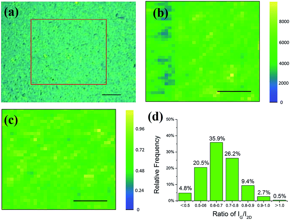 | ||
| Fig. 3 (a) Optical photograph of continuous graphenes on silicon substrate after nickel etched off. The Inset red rectangle refers to the area of Raman mapping corresponding to (b) and (c). (b) Raman mapping of G peak intensity. (c) Raman mapping of the ratio of IG/I2D over the same area as that in (b). (d) Statistical chart of IG/I2D over 1000 points. Scale bars, 20 μm. | ||
In addition, TEM characterization is used to confirm the high quality of obtained graphenes. As shown in Fig. 4a, the obtained graphenes on SiO2/Si substrate have continuous and uniform morphology (continuous and with no cracks) which suggest good crystallization of carbon atoms.31 In Fig. 4b–d, HRTEM (High Resolution Transmission Electron Microscopy) images demonstrates that obtained graphene have about 5 layers.
 | ||
| Fig. 4 (a) TEM image of graphenes obtained from silicon substrate after growth. (b), (c) and (d) HRTEM images of few-layered graphene. | ||
3.3 Graphene synthesized by different thickness of nickel film on silicon substrates
Nickel film, as the catalyst during the synthesis, plays a critical role in our experiment. Therefore we also study the relation of graphene's quality and nickel's thickness. Fig. 5a compares the Raman spectra of graphene synthesized by different thickness of nickel film, in which the thickness of nickel range from 25 to 700 nm. On the condition of 25 and 50 nm, most nickel evaporated or de-wetted during the flame heating process. Despite that, very weak G and 2D bands can still be detected in the samples with 25 and 50 nm thick nickel. Once nickel film is over 100 nm, the possibility of dewetting of Ni is eliminated and carbon can out-diffuse through Ni and form continuous graphene film at the interface of Ni and silicon substrates. When Ni is over 100 nm, graphenes obtained with different thickness of Ni still exhibit slightly different Raman signals, in which 400–500 nm nickel can produce graphenes with best quality. Obvious D peaks can be found in the samples with 100–300 nm Ni, while 2D peaks with relatively wide full-widths at half-height maximum (FWHM) can be found in the samples with 600–700 nm Ni. Fig. 5b exhibits statistic correlation of nickel's thickness and ratios of ID/IG and IG/I2D. Ratios of IG/I2D of obtained graphene are between 0.8 and 1.8, indicating that the productions contain bi-layer and few layer graphene.32,33 | ||
| Fig. 5 (a) Raman spectra of the graphene synthesized by different thickness of nickel film (25, 50, 100–700 nm). (b) The ratios of ID/IG and IG/I2D of the graphene growth from different thickness of nickel film. | ||
4. Concluding
Our dual flame method is a fast, productive and economical method to directly synthesize high quality graphenes on dielectric substrate without transfer process in open environments. It involves only one single step process to produce few-layer graphenes and needs only dozen seconds of whole growth procedure. Relatively good quality of continuous bi-layer and few layer graphenes can be obtained directly on SiO2/Si substrate. Considering its high efficiency, energy saving and low cost, it will have chance to significantly contribute to practical applications of graphene in the future.Acknowledgements
This work was supported by National Science Foundation of China (Grant nos 10774032, 90921001), Key Knowledge Innovation Project of the Chinese Academy of Sciences on Water Science Research, Instrument Developing Project of the Chinese Academy of Sciences (Grant no. Y2010031).Notes and references
- K. S. Novoselov, A. K. Geim, S. V. Morozov, D. Jiang, Y. Zhang, S. V. Dubonos, I. V. Grigorieva and A. A. Firsov, Science, 2004, 306, 666–669 CrossRef CAS PubMed.
- M. Ishigami, J. H. Chen, W. G. Cullen, M. S. Fuhrer and E. D. Williams, Nano Lett., 2007, 7, 1643–1648 CrossRef CAS PubMed.
- K. I. Bolotin, K. J. Sikes, Z. Jiang, M. Klima, G. Fudenberg, J. Hone, P. Kim and H. L. Stormer, Solid State Commun., 2008, 146, 351–355 CrossRef CAS PubMed.
- Y. C. Huang, C. P. Chang and M. F. Lin, Nanotechnology, 2007, 18, 495401 CrossRef CAS PubMed.
- A. A. Balandin, S. Ghosh, W. Bao, I. Calizo, D. Teweldebrhan, F. Miao and C. N. Lau, Nano Lett., 2008, 8, 902–907 CrossRef CAS PubMed.
- D. A. Dikin, S. Stankovich, E. J. Zimney, R. D. Piner, G. H. Dommett, G. Evmenenko, S. T. Nguyen and R. S. Ruoff, Nature, 2007, 448, 457–460 CrossRef CAS PubMed.
- Y. Hernandez, V. Nicolosi, M. Lotya, F. M. Blighe, Z. Sun, S. De, I. T. McGovern, B. Holland, M. Byrne, Y. K. Gun'Ko, J. J. Boland, P. Niraj, G. Duesberg, S. Krishnamurthy, R. Goodhue, J. Hutchison, V. Scardaci, A. C. Ferrari and J. N. Coleman, Nat. Nanotechnol., 2008, 3, 563–568 CrossRef CAS PubMed.
- X. Li, W. Cai, J. An, S. Kim, J. Nah, D. Yang, R. Piner, A. Velamakanni, I. Jung, E. Tutuc, S. K. Banerjee, L. Colombo and R. S. Ruoff, Science, 2009, 324, 1312–1314 CrossRef CAS PubMed.
- S. Bae, H. Kim, Y. Lee, X. Xu, J. S. Park, Y. Zheng, J. Balakrishnan, T. Lei, H. R. Kim, Y. I. Song, Y. J. Kim, K. S. Kim, B. Ozyilmaz, J. H. Ahn, B. H. Hong and S. Iijima, Nat. Nanotechnol., 2010, 5, 574–578 CrossRef CAS PubMed.
- Z. Sun, Z. Yan, J. Yao, E. Beitler, Y. Zhu and J. M. Tour, Nature, 2010, 468, 549–552 CrossRef CAS PubMed.
- G. Kalita, K. Wakita and M. Umeno, RSC Adv., 2012, 2, 2815–2820 RSC.
- N. Liu, L. Fu, B. Dai, K. Yan, X. Liu, R. Zhao, Y. Zhang and Z. Liu, Nano Lett., 2011, 11, 297–303 CrossRef CAS PubMed.
- H. Huang, W. Chen, S. Chen and A. T. S. Wee, ACS Nano, 2008, 2, 2513–2518 CrossRef CAS PubMed.
- L. Jiao, L. Zhang, X. Wang, G. Diankov and H. Dai, Nature, 2009, 458, 877–880 CrossRef CAS PubMed.
- F. Yu, H. Q. Zhou, Z. X. Zhang, D. S. Tang, M. J. Chen, H. C. Yang, G. Wang, H. F. Yang, C. Z. Gu and L. F. Sun, Appl. Phys. Lett., 2012, 100, 101904 CrossRef PubMed.
- B. M. Kellie, A. C. Silleck, K. Bellman, R. Snodgrass and S. Prakash, RSC Adv., 2013, 3, 7100–7105 RSC.
- N. K. Memon, F. S. Xu, G. L. Sun, S. J. B. Dunham, B. H. Kear and S. D. Tse, Carbon, 2013, 63, 478–486 CrossRef CAS PubMed.
- Z. Li, H. W. Zhu, D. Xie, K. L. Wang, A. Y. Cao, J. Q. Wei, X. A. Li, L. L. Fan and D. H. Wu, Chem. Commun., 2011, 47, 3520–3522 RSC.
- N. K. Memon, S. D. Tse, J. F. Al-Sharab, H. Yamaguchi, A. M. B. Goncalves, B. H. Kear, Y. Jaluria, E. Y. Andrei and M. Chhowalla, Carbon, 2011, 49, 5064–5070 CrossRef CAS PubMed.
- R. N. Tiwari, M. Ishihara, J. N. Tiwari and M. Yoshimura, J. Mater. Chem., 2012, 22, 15031 RSC.
- A. C. Ferrari, J. C. Meyer, V. Scardaci, C. Casiraghi, M. Lazzeri, F. Mauri, S. Piscanec, D. Jiang, K. S. Novoselov, S. Roth and A. K. Geim, Phys. Rev. Lett., 2006, 97, 187401 CrossRef CAS.
- M. S. Dresselhaus, G. Dresselhaus, R. Saito and A. Jorio, Phys. Rep., 2005, 409, 47–99 CrossRef PubMed.
- A. Reina, S. Thiele, X. T. Jia, S. Bhaviripudi, M. S. Dresselhaus, J. A. Schaefer and J. Kong, Nano Res., 2009, 2, 509–516 CrossRef CAS.
- Q. K. Yu, J. Lian, S. Siriponglert, H. Li, Y. P. Chen and S. S. Pei, Appl. Phys. Lett., 2008, 93, 113103 CrossRef PubMed.
- Z. W. Peng, Z. Yan, Z. Z. Sun and J. M. Tour, ACS Nano, 2011, 5, 8241–8247 CrossRef CAS PubMed.
- J. S. Chen, B. Wu and Y. Q. Liu, Acta Chim. Sin., 2014, 72, 359–366 CrossRef CAS.
- S. J. Chae, F. Gunes, K. K. Kim, E. S. Kim, G. H. Han, S. M. Kim, H. J. Shin, S. M. Yoon, J. Y. Choi, M. H. Park, C. W. Yang, D. Pribat and Y. H. Lee, Adv. Mater., 2009, 21, 2328–2333 CrossRef CAS.
- A. Reina, X. Jia, J. Ho, D. Nezich, H. Son, V. Bulovic, M. S. Dresselhaus and J. Kong, Nano Lett., 2009, 9, 30–35 CrossRef CAS PubMed.
- Y. Y. Wang, Z. H. Ni, T. Yu, Z. X. Shen, H. M. Wang, Y. H. Wu, W. Chen and A. T. S. Wee, J. Phys. Chem. C, 2008, 112, 10637–10640 CAS.
- A. Ismach, C. Druzgalski, S. Penwell, A. Schwartzberg, M. Zheng, A. Javey, J. Bokor and Y. Zhang, Nano Lett., 2010, 10, 1542–1548 CrossRef CAS PubMed.
- L. H. Tang, H. B. Feng, J. S. Cheng and J. H. Li, Chem. Commun., 2010, 46, 5882–5884 RSC.
- Z. Q. Luo, T. Yu, J. Z. Shang, Y. Y. Wang, S. Lim, L. Liu, G. G. Gurzadyan, Z. X. Shen and J. Y. Lin, Adv. Funct. Mater., 2011, 21, 911–917 CrossRef CAS.
- J. S. Park, A. Reina, R. Saito, J. Kong, G. Dresselhaus and M. S. Dresselhaus, Carbon, 2009, 47, 1303–1310 CrossRef CAS PubMed.
| This journal is © The Royal Society of Chemistry 2015 |