DOI:
10.1039/C4RA13317J
(Paper)
RSC Adv., 2015,
5, 6906-6911
Size effect of InAs quantum dots grown by metal organic chemical vapor deposition technique in storing electrical charges for memory applications
Received
28th October 2014
, Accepted 16th December 2014
First published on 17th December 2014
Abstract
Catalyst-free growth of InAs quantum dots (QDs) with different sizes and densities was undertaken by metal organic chemical vapor deposition technique to investigate their capability and the effect of size on charge storage. The QDs were grown on a high-k dielectric, ZrO2, layer, which was deposited onto the GaAs substrate passivated with an ultra-thin GaP layer. The size and density of the QDs were controlled by varying the growth temperature. To demonstrate the effect of QD dot size on charge storage behavior, they were used as charge storing nodes in a GaAs metal-oxide–semiconductor based memory device. From capacitance–voltage measurements, it was observed that the hysteresis width of the device and the density of stored charge increase with a decrease in size of the QDs. This is due to size quantization, for which the surface potential as well as the generation of strongly localized trap levels become significant. On the other hand, the charge retention is found to increase on increasing the dot size due to enhanced conduction band offset between the QDs and the substrate, in which tunneling back the stored carriers is minimized.
1 Introduction
The quantum size effect (QSE) is one of the most pronounced effects in quantum confined semiconductor nanostructures when the size of the nanocrystals (NCs) is smaller than the electron de Broglie wavelength. QSE facilitates the formation of electric dipoles, redistribution or localization of the energy levels, and leads to a discrete density of states along the confinement direction.
However, the quantum size effect causes widening of the bandgap as well as a change in the density of states of the semiconductor NCs. Moreover, due to the size effect, the variation of surface potential promoted by electrostatic coulomb charging is observed along with carrier tunneling. Size quantization favors the charging of discrete energy levels of the NCs and when the total capacitance of the NCs is sufficiently small, the coulomb blockade effect becomes significant. The coulomb blockade effect prevents further electron to tunnel into the NCs because in that case addition of single electron requires sufficient charging energy. Coulomb blockade effect, thus, minimize the leakage current by reducing the carrier tunneling. Therefore, the QSE plays a crucial role on the capacitance of a semiconductor NCs and thus the charge storage properties of the NCs are affected to a great extent.
Recently, effect of particle size on the resonant tunneling phenomena in CdS nanoparticles (NPs) based electrical bistability devices was reported by Nenna et al.1 The current conduction and negative differential resistance behavior produced by resonant tunneling effect was significantly enhanced due to the formation of quantized energy levels by decreasing the size of the CdS NPs. Yun et al.2 reported the size dependent single electron tunneling phenomena in Pt NPs embedded metal-oxide–semiconductor (MOS) structure at room temperature. On reducing the (Pt) particle size, the single electron addition energy (coulomb charging energy) has been found to increase leading to larger tunneling current. The QSE on the surface potential of nanocrystalline Si based thin film transistor was reported by Mao.3 Here the change in surface potential of the Si–NCs was investigated due to the change in bandgap as well dielectric constant with the grain size. The dependency of gate leakage current on the grain size of Si–NCs was also studied by Mao.4 Here the author demonstrated that the tunneling current of Si thin film transistor strongly depends on the size of Si–NCs due to the change in surface potential.
Though some reports are available in the literature about the size effect of nanostructures on charge storage, most of these devices are based on the Si metal-oxide–semiconductor (MOS) structure using Si5 and Ge NCs.6,7 It is found from these reports that the stored charge density and the carrier dynamics in terms of charge retention time were uniquely controlled with the size of NCs in the memory devices. However due to superior electron transport properties, viz. high electron mobility and high break down field of GaAs compared to Si; GaAs MOS based structures are considered to be a better choice for new generation low-power and high-speed memory applications.8–10 In order to reduce the operating voltage various high-k dielectric materials, viz. HfO2, ZrO2, Al2O3, Y2O3, TiO2, and LaAlO3 are used in the MOS structures.11–17
In the literature various studies are available where semiconductor nanostructures such as Si,18 Ge,19,20 SiGe QDs,21 Si nano-needles,22 and carbon nanotubes23 were used as charge storing nodes. Metallic nanoparticles of Ni,24 Pt,25 cobalt silicide (CoSi2),26 vanadium silicide (V3Si),27 and AuPd,28 and dielectric NCs (such as Al2O3 nanodots),29 were also used as charge storing elements. In these reports, though the authors studied the charge storing capability of NCs, QDs, and metallic NPs, the effect of size quantization is not investigated. Moreover use of metallic nanoparticles leads to reaction between the metal and oxide. In some cases, metal might diffused into the oxide matrix and due to high temperature processing, it gets ionized leading to doping the gate, source or drain region.30 Moreover obtaining stable metal NPs with repeatability is not an easy task. Furthermore any application with metal NPs does not fit in the existing process lines of IC technology. Thus semiconducting QDs are good substitutes for metal NPs as charge storage elements since the former has certain advantages of high exciton binding energy, minibands, and large discrete density of states which makes it suitable for multibit storage. Reports are available where single layer InAs QDs was used as charge storage nodes in GaAs/AlGaAs heterostructure.31 However type-I nature of InAs/GaAs heterostructure promotes rapid unwanted radiative recombination of carriers. As a result charge storage relaxation takes place, which deteriorates the charge retention characteristics of the memory devices.
In order to achieve good retention property, it is important to have high conduction band offset between QDs and the high-k dielectric materials in MOS based memory devices along with good interface quality with the tunnel layer. It is well known that like SiO2/Si, the direct deposition of high-k dielectric layer on GaAs does not facilitate stable and defect free interface due to the presence of surface states as a result of Ga–O or As–O bonds which will lead to large surface recombination velocity and Fermi level pinning. Thus proper surface passivation is essential for the realization of high performance stable GaAs MOS devices. Hence to eliminate the native oxide formation and to unpin the Fermi level, in this work, an ultra-thin GaP layer was grown on GaAs. If we consider InAs QDs (electron affinity of 4.9 eV) for the purpose, it is found that InAs/ZrO2 interface offers a barrier height of about 3.26 eV. In this work, we have thus introduced InAs QDs along with high-k dielectric (ZrO2) to obtain GaAs MOS based memory structures to engineer the band offsets. Due to small energy bandgap and small carrier effective mass, there exists well splitted energy levels in InAs QDs, which favors multibit data storage.32 In this paper, we, thus, report the catalyst-free size controlled growth and characterization of InAs QDs on high-k dielectric (ZrO2) layers to explore its capability of charge storage while using it in a GaAs MOS based memory device.
2 Experimental
p-Type (100) GaAs substrates, having carrier concentration of 1 × 1016 cm−3, were chemically surface treated by boiling sequentially with acetone and methanol followed by rinsing repeatedly in deionized water (18.2 MΩ). Then the substrates were dipped into the etchant solution of H2O2–NH4OH–H2O (1![[thin space (1/6-em)]](https://www.rsc.org/images/entities/char_2009.gif) :1:2 by volume) in order to remove native oxide and elemental As. Finally those were rinsed for 3 min in deionized water and dried by N2 gun. An ultra-thin interface passivation layer (IPL) of GaP of thickness 1.6 ± 0.3 nm was grown on p-GaAs at 540 °C by metal organic chemical vapor deposition (MOCVD) technique. Tri-methyl gallium (TMGa) and phosphine (PH3), with a flow rate of 6.8 sccm and 70 sccm, respectively, were used as the precursors for Ga and P, respectively, whereas high purity H2 was used as carrier gas. Then ZrO2 (5 nm thick) was grown on it as a tunneling layer. Zirconium t-butoxide [Zr-(OC4H9)4] and O2 were used as the zirconia and oxide precursors, respectively. Here the growth was performed at 300 °C and N2 was used as the carrier gas. The grown ZrO2 film was annealed at 500 °C for 5 min in N2 ambient. The growth of InAs QDs with different sizes on tunneling ZrO2 was carried out for 2 min by MOCVD technique at different temperatures as shown in Table 1. Tri-methyl indium (TMI) and arsine (AsH3) were utilized as the precursors for In and As, respectively. The flow rate of TMI and AsH3 were taken as 45 and 75 sccm, respectively. Finally ZrO2 control layer of thickness 25 nm was deposited. Top gate electrode of Al covering an area 1.96 × 10⁻³ cm2 was formed by thermal evaporation. Similarly a low resistance ohmic contact was made with Pd–Ag onto the back surface of GaAs. It was then annealed at 300 °C for 3 min in argon ambience. The thickness of the deposited layers was determined by an ellipsometer (Accurion Nanofilm EP3 Model). Atomic force microscopy (AFM) (model 5100, Agilent Technologies) was used to determine the size and density of QDs grown on tunneling layer. The QDs were also characterized by high resolution transmission electron microscope (HRTEM, Jeol Jem-2100) and TEM (FEI-Tecnai G220S-Twin). The chemical analysis of the QDs was made by X-ray photoelectron spectroscopy (XPS) using PHI 5000 VersaProbeII (ULVAC-PHI, INC, Japan) system attached with a microfocused (100 μm, 25 W, 15 kV) monochromatic Al Kα source (hν = 1486.6 eV), a hemispherical analyzer, and a multichannel detector. The vacuum was maintained at ∼10−11 torr inside the chamber throughout the experiment. To neutralize the charge, a combination of low energy Ar+ ions and electrons were used during the analysis. Charge calibration of the binding energy scale was done by C 1s peak at 284.6 eV. The electrical measurements of the memory devices were carried out using Keithley (4200-SCS) semiconductor parameter analyzer.
:1:2 by volume) in order to remove native oxide and elemental As. Finally those were rinsed for 3 min in deionized water and dried by N2 gun. An ultra-thin interface passivation layer (IPL) of GaP of thickness 1.6 ± 0.3 nm was grown on p-GaAs at 540 °C by metal organic chemical vapor deposition (MOCVD) technique. Tri-methyl gallium (TMGa) and phosphine (PH3), with a flow rate of 6.8 sccm and 70 sccm, respectively, were used as the precursors for Ga and P, respectively, whereas high purity H2 was used as carrier gas. Then ZrO2 (5 nm thick) was grown on it as a tunneling layer. Zirconium t-butoxide [Zr-(OC4H9)4] and O2 were used as the zirconia and oxide precursors, respectively. Here the growth was performed at 300 °C and N2 was used as the carrier gas. The grown ZrO2 film was annealed at 500 °C for 5 min in N2 ambient. The growth of InAs QDs with different sizes on tunneling ZrO2 was carried out for 2 min by MOCVD technique at different temperatures as shown in Table 1. Tri-methyl indium (TMI) and arsine (AsH3) were utilized as the precursors for In and As, respectively. The flow rate of TMI and AsH3 were taken as 45 and 75 sccm, respectively. Finally ZrO2 control layer of thickness 25 nm was deposited. Top gate electrode of Al covering an area 1.96 × 10⁻³ cm2 was formed by thermal evaporation. Similarly a low resistance ohmic contact was made with Pd–Ag onto the back surface of GaAs. It was then annealed at 300 °C for 3 min in argon ambience. The thickness of the deposited layers was determined by an ellipsometer (Accurion Nanofilm EP3 Model). Atomic force microscopy (AFM) (model 5100, Agilent Technologies) was used to determine the size and density of QDs grown on tunneling layer. The QDs were also characterized by high resolution transmission electron microscope (HRTEM, Jeol Jem-2100) and TEM (FEI-Tecnai G220S-Twin). The chemical analysis of the QDs was made by X-ray photoelectron spectroscopy (XPS) using PHI 5000 VersaProbeII (ULVAC-PHI, INC, Japan) system attached with a microfocused (100 μm, 25 W, 15 kV) monochromatic Al Kα source (hν = 1486.6 eV), a hemispherical analyzer, and a multichannel detector. The vacuum was maintained at ∼10−11 torr inside the chamber throughout the experiment. To neutralize the charge, a combination of low energy Ar+ ions and electrons were used during the analysis. Charge calibration of the binding energy scale was done by C 1s peak at 284.6 eV. The electrical measurements of the memory devices were carried out using Keithley (4200-SCS) semiconductor parameter analyzer.
Table 1 InAs QDs with different sizes and densities at different growth temperature using MOCVD technique
| Sample |
QDs diameter (nm) |
QDs density (cm−2) |
Growth temperature (°C) |
| AFM |
TEM |
| A |
5 |
4 |
2.00 × 10¹¹ |
500 |
| B |
12.5 |
12 |
1.68 × 10¹¹ |
550 |
| C |
16 |
15 |
1.00 × 10¹¹ |
580 |
3 Results and discussion
3.1. Characterizations of InAs QDs
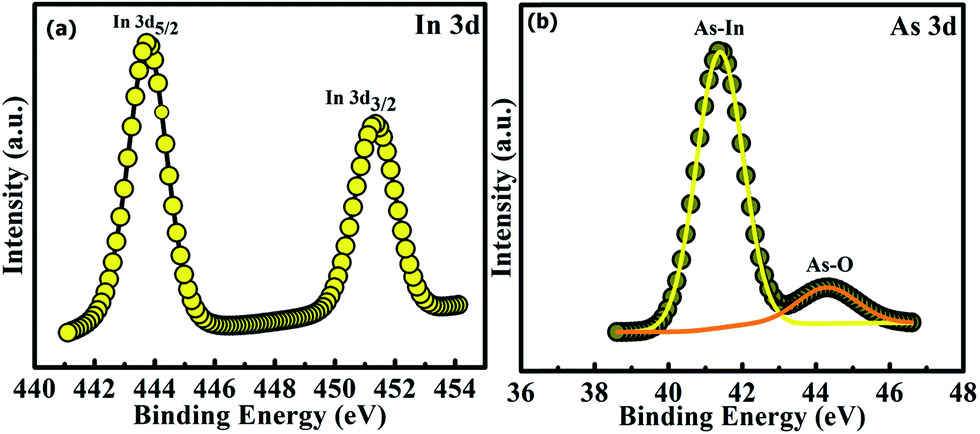
The AFM images of InAs QDs which is homogeneously distributed over the surface of high-k corresponding to the samples A, B, and C are shown in Fig. 1(a)–(c), respectively. With the help of WSxM software, relevant parameters of the grown QDs are determined and presented in Table 1. Fig. 2(a)–(c) represent the plan-view bright field TEM micrograph of the quantum dots with approximately round in shape and the average dot diameter was found to be 4, 12, and 15 nm, respectively. The obtained values of the dot diameter from the TEM image were found to be smaller than the AFM images. This can be attributed to the tip size convolution. As the AFM tip cannot penetrate the region between two closely spaced QDs, so the size of the QDs was found to be higher than the value obtained from TEM images. Because of the enhanced migration length and increased adsorption with increasing temperature, indium (In) adatoms become more mobile and hence promote rapid nucleation. Thus the size and density of the QDs changes with increasing growth temperature. The chemical nature of InAs QDs and ZrO2 was analyzed by high resolution XPS measurements. As depicted in Fig. 3(a), two distinct peaks of In 3d spectrum of the InAs QDs are observed.
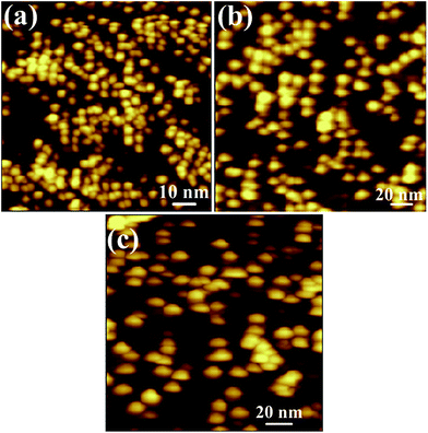 |
| | Fig. 1 AFM images of MOCVD grown InAs QDs on tunneling ZrO2 at a substrate temperature of (a) 500 °C, (b) 550 °C and (c) 580 °C. | |
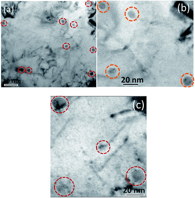 |
| | Fig. 2 TEM images of the MOCVD grown InAs QDs on tunneling ZrO2 at (a) 500 °C (b) 550 °C and (c) 580 °C substrate temperatures. | |
 |
| | Fig. 3 X-ray photoelectron spectra of (a) In 3d and (b) the As 3d region of InAs QDs. | |
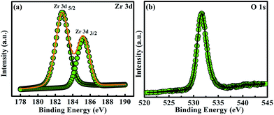
The one located at 443.80 eV belongs to In 3d5/2, while the other at 451.40 eV corresponds to In 3d3/2. Thus the value of spin orbital splitting (SOS) was found to be 7.60 eV. Fig. 3(b) shows the signature of two peaks of As. The peak at 41.40 eV is related to As whereas that at 44.40 eV denotes the oxidized As. The As peak was found to be more stronger than that obtained from the oxidized species. The spectrum of Zr 3d signal of ZrO2 films is shown in Fig. 4(a). Two peaks of Zr 3d signal corresponding to Zr 3d5/2 and Zr 3d3/2 are located at 182.80 eV and 185.10 eV. The SOS value was found to be 2.3 eV which assured the fully oxidation state of Zr (Zr+4).33 The presence of O 1s core level spectrum at 532.15 eV as shown in Fig. 4(b) again confirms the formation of ZrO2 film.
 |
| | Fig. 4 X-ray photoelectron spectra of (a) Zr 3d and (b) O 1s. The annealing of the grown ZrO2 film was done at 500 °C for 5 min in N2 ambient. | |
3.2. QDs as charge storage nodes
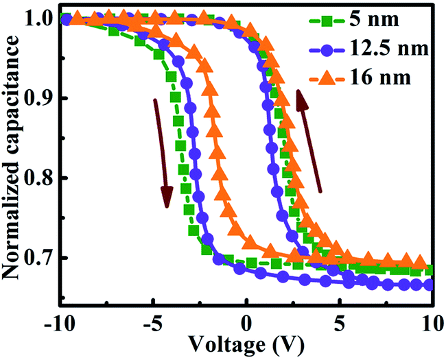
The MOCVD grown InAs QDs are used as charge storage elements in a GaAs MOS based memory device. Fig. 5(a) and (b) shows the schematic view of a typical GaAs MOS based non-volatile memory device with InAs QDs embedded between the high-k control and tunneling ZrO2 dielectric layers and cross-sectional TEM image of the device, respectively. The HRTEM images of the InAs QDs on the high-k dielectric and the presence of native oxide layer on the surface of InAs QDs are shown in Fig. 5(c) and (d), respectively. The charge storage behavior was studied at room temperature through high-frequency (1 MHz) capacitance–voltage characteristics (C–V) at a gate sweeping voltage of ±10 V. As shown in Fig. 6, memory windows of width 6.81, 4.32, and 3.89 V were observed in the memory cells using QD samples A, B, and C, respectively. The hysteresis width of the memory device is found to decrease with increase in dot size. Due to profound change in density of states in QDs, the density of stored charge (Dcharge) increases with decrease in dot size (dQD) and which follows from the following relations:| |
 | (1) |
and| | |
Memory window ∝ Dcharge
| (2) |
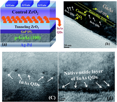 |
| | Fig. 5 (a) A schematic of the device structure and (b) cross-sectional TEM image of InAs QDs embedded in a matrix of ZrO2. HRTEM images of the (c) InAs QDs and (d) native oxide layer on the surface of InAs QDs. | |
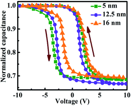 |
| | Fig. 6 Room temperature high-frequency (1 MHz) capacitance–voltage characteristics of the GaAs NVM devices containing InAs QDs with sizes 5, 12.5, and 16 nm corresponding to the growth temperature 500, 550, and 580 °C, respectively. | |
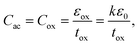
Moreover gradual increase in surface potential with decreasing dot size at a particular gate voltage will also lead to increase in stored charge density. For smaller dots, the generation of strongly localized trap levels becomes significant which in turn will increase the stored charge density into the QDs. However, the hysteresis in C–V characteristics can be obtained either due to the injection of charges into the trap sites of the InAs QDs or due to the presence of interface states. Again the counter clockwise hysteresis direction suggests that the carrier transport between InAs QDs and p-type GaAs substrate is due to tunneling.26 To ensure that the origin of charge storage is the QDs, we have characterized our memory devices by frequency dependent C–V measurements. No frequency dispersion in accumulation capacitance is found and nearly constant hysteresis width was observed as shown in Fig. 7(a)–(c), for the memory cells made of QD samples A, B, and C, respectively, when the frequency was varied from 50 kHz to 1 MHz at ±10 V. This confirms that the hysteresis found in the C–V characteristics is due the presence of QDs and not due to the generation of trap charges in ZrO2 or ZrO2/GaAs interface. The maximum capacitance at the leftmost voltage (most negative) is the accumulation capacitance (Cac), i.e. oxide capacitance (Cox) as shown in Fig. 7(a)–(c). The capacitance per unit area of the MOS capacitor under accumulation region is the oxide capacitance which can be expressed as:
| |
 | (3) |
where
k is the permittivity,
ε0 is the free space permittivity and
tox is the gate dielectric thickness. The thickness (
tox) of the high-
k dielectric layer (ZrO
2 in our case) is kept constant in all the devices containing three different sizes QDs. As the MOCVD grown InAs QDs are embedded (not incorporated) between the high-
k oxide layers, so there is no change in the stoichiometry of the oxide. Hence the material property,
i.e. the dielectric permittivity (
k) is not changed. As a result maximum capacitance,
i.e. accumulation capacitance is found to be almost same in all the devices. It depends only on the applied voltage irrespective of QDs size and frequency. However the slight variation in the oxide capacitance, as shown in
Fig. 7(a)–(c) is due to the change in effective oxide thickness. On the other hand, the QDs act as charge storage elements which are responsible only for the shift in flatband voltage,
i.e. memory window during voltage sweeping. Thus change in the size of InAs QDs has lead to change in the flatband voltage or in other words to change the memory window. The programming (writing) and erasing operation were explained in terms of band diagram as shown in
Fig. 8(a) and (b), respectively. The programming,
i.e. writing operation is achieved during the application of positive voltage at the gate electrode. In this condition the inversion electrons of the GaAs side will tunnel from the GaAs conduction band to the InAs QDs. The injected electrons are then stored into the deep trap sites of InAs QDs leading to the writing operations. Again further movement of electrons towards the metal gate electrode is inhibited due to the thick control high-
k dielectric layer. However during erasing operation the trapped electrons are emitted back to the GaAs on applying negative voltage to the gate electrode. The injection of holes from GaAs to InAs QDs becomes significant under erasing condition leading to large hole current. During erase cycle the electron current from the gate electrode was minimized by using high-
k dielectric (ZrO
2) which acts as a blocking layer. However the back tunneling current (the current dominated by holes under programming mode and the current promoted by electrons under erasing mode) can be suppressed by using ZrO
2 as a blocking oxide layer, which exhibits large barrier height along with large relative permittivity.
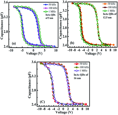 |
| | Fig. 7 Room temperature frequency dependent capacitance–voltage characteristics of the GaAs MOS based NVM devices containing InAs QDs with sizes (a) 5 nm, (b) 12.5 nm, and (c) 16 nm with sweeping gate voltage ±10 V. No frequency dispersion was found in the InAs QDs embedded memory devices. This ensures the obtained memory effect is due to the charge storage in the InAs QDs. | |
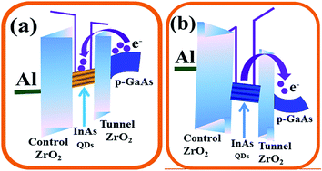 |
| | Fig. 8 Schematic energy band diagram of Al/ZrO2/InAs QDs/ZrO2/(GaP)p-GaAs memory structure at (a) positive programming bias condition, and (b) negative bias for erasing modes. | |
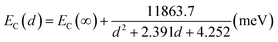
The charge storage behavior of the device was investigated in terms of discharging mechanism of the charges in the InAs QDs and thus the capacitance decay was determined. From Fig. 9, the retention of the stored charge was found to be better with QD samples C. With increase in the size of the QDs, the conduction band shifts towards the lower energy compared to its bulk counterpart resulting in increase in the conduction band offset between QDs and the surrounding oxide according to the following relation6,34,35 assuming spherical InAs QDs of diameter d in nm:
| |
 | (4) |
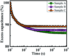 |
| | Fig. 9 Charge retention characteristics of the GaAs MOS based NVM devices of samples A, B, and C. | |
Hence the emission of existing stored charge carriers, i.e. back tunneling current from QDs to the substrate is suppressed. As a result the capacitance decay is reduced. Therefore the charge retention into the QDs is enhanced with increase in the size of the QDs. As shown in Fig. 9, there exist two capacitance decay regions, viz. initial fast decay and then slow decay region. Lateral charge spreading and Coulomb repulsion is responsible for the initial fast charge loss in the device while slow decay is caused due to the charge leakage through the tunnel layer. Since high growth temperature promotes the localization of QDs, initial decay is slightly minimized with increasing the size of QDs. However it was also seen that the leakage through tunneling was significantly reduced for the devices consists of QDs with bigger sizes which were grown at higher temperature leading to less generation of interface trap states.
4 Conclusion
We have successfully achieved the size controlled growth of InAs QDs by MOCVD technique on high-k ZrO2, which is deposited onto the ultra-thin GaP passivated p-GaAs (100) substrates. From AFM and TEM images it was found that the average size of the QDs increases whereas its density decreases with increase in growth temperature. We have systematically studied the effect of the size of InAs QDs on the charge storage characteristics in GaAs MOS based non-volatile flash memory devices. Superior memory window was obtained when the size of QDs is 5 nm, whereas the charge retention is found to be enhanced with increase in QDs size on increasing growth temperature. Thus a trade-off in size of the QDs is required for an optimum memory operation.
Acknowledgements
One of the authors (SMI) acknowledges financial support from University Grants Commission, New Delhi through Maulana Azad National Fellowship for Minority Students. The authors are also thankful to Prof. Rabibrata Mukherjee, Department of Chemical Engineering, IIT Kharagpur for AFM measurements.
References
- G. Nenna, S. Masala, V. Bizzarro, M. Re, E. Pesce, C. Minarini and T. D. Luccio, J. Appl. Phys., 2012, 112, 044508 CrossRef PubMed.
- M. Yun, B. Ramalingam and S. Gangopadhyay, Nanotechnology, 2011, 22, 465201 CrossRef PubMed.
- L. F. Mao, Thin Solid Films, 2010, 518, 3396 CrossRef CAS PubMed.
- L. F. Mao, J. Vac. Sci. Technol., B: Microelectron. Nanometer Struct.–Process., Meas., Phenom., 2010, 28, 460 CrossRef CAS.
- R. A. Rao, H. P. Gasquet, R. F. Steimle, G. Rinkenberger, S. Straub, R. Muralidhar, S. G. H. Anderson, J. A. Yater, J. C. Ledezma, J. Hamilton, B. Acred, C. T. Swift, B. Hradsky, J. Peschke, M. Sadd, E. J. Prinz, K. M. Chang and B. E. White Jr, Solid-State Electron., 2005, 49, 1722 CrossRef CAS PubMed.
- L. F. Mao, Nanoscale Res. Lett., 2013, 8, 21 CrossRef PubMed.
- A. E. Hdiy, K. Gacem, M. Troyon, A. Ronda, F. Bassani and I. Berbezier, J. Appl. Phys., 2008, 104, 063716 CrossRef PubMed.
- K. Y. Cheng, M. Feng, D. Cheng and C. Liao, in Fundamentals of III–V semiconductor MOSFETs, ed. S. Oktyabrsky and P. D. Ye, Springer, New York, 2010, ch. 10, pp. 285–305 Search PubMed.
- R. C. Jeff Jr, M. Yun, B. Ramalingam, B. Lee, V. Misra, G. Triplett and S. Gangopadhyay, Appl. Phys. Lett., 2011, 99, 072104 CrossRef PubMed.
- H. C. Chiu, C. K. Lin, C. W. Lin and C. S. Lai, Microelectron. Reliab., 2012, 52, 2592 CrossRef CAS PubMed.
- H. S. Kim, I. Ok, M. Zhang, F. Zhu, S. Park, J. Yum, H. Zhao and J. C. Lee, Appl. Phys. Lett., 2007, 91, 042904 CrossRef PubMed.
- G. K. Dalapati, Y. Tong, W. Y. Loh, H. K. Mun and B. J. Cho, IEEE Trans. Electron Devices, 2007, 54, 1831 CrossRef CAS.
- J. Oh, P. Majhi, C. Y. Kang, J. W. Yang, H. H. Tseng and R. Jammy, Appl. Phys. Lett., 2007, 90, 202102 CrossRef PubMed.
- P. D. Ye, G. D. Wilk, J. Kwo, B. Yang, H.-J. L. Gossmann, M. Frei, S. N. G. Chu, J. P. Mannaerts, M. Sergent, M. Hong, K. K. Ng and J. Bude, IEEE Electron Device Lett., 2003, 24, 209 CrossRef CAS.
- G. D. Wilk, R. M. Wallace and J. M. Anthony, J. Appl. Phys., 2001, 89, 5243 CrossRef CAS PubMed.
- M. K. Lee, C. F. Yen and J. J. Huang, J. Electrochem. Soc., 2006, 153, F77 CrossRef CAS PubMed.
- D. Choi, J. S. Harris, M. Warusawithana and D. G. Schlom, Appl. Phys. Lett., 2007, 90, 243505 CrossRef PubMed.
- H. I. Hanafi, S. Tiwari and I. Khan, IEEE Trans. Electron Devices, 1996, 43, 1553 CrossRef CAS.
- S. Das, K. Das, R. K. Singha, A. Dhar and S. K. Ray, Appl. Phys. Lett., 2007, 91, 233118 CrossRef PubMed.
- K. Das, M. Nanda Goswami, R. Mahapatra, G. S. Kar, A. Dhar, H. N. Acharya, S. Maikap, J. H. Lee and S. K. Ray, Appl. Phys. Lett., 2004, 84, 1386 CrossRef CAS PubMed.
- D. W. Kim, F. E. Prins, D. L. Kwong and S. K. Banerjee, IEEE Trans. Electron Devices, 2003, 50, 510 CrossRef CAS.
- S. Jung, J. Yoo, Y. Kim, S. K. Dhungel and J. Yi, Mater. Sci. Eng., C, 2006, 26, 813 CrossRef CAS PubMed.
- X. B. Lu and J. Y. Dai, Appl. Phys. Lett., 2006, 88, 113104 CrossRef PubMed.
- D. Panda, S. Maikap, A. Dhar and S. K. Ray, Electrochem. Solid-State Lett., 2009, 12, H7 CrossRef CAS PubMed.
- H. Kim, S. Woo, H. Kim, S. Bang, Y. Kim, D. Choi and H. Jeon, Electrochem. Solid-State Lett., 2009, 12, H92 CrossRef CAS PubMed.
- J. H. Kim, J. Y. Yang, J. S. Lee and J. P. Hong, Appl. Phys. Lett., 2008, 92, 013512 CrossRef PubMed.
- D. Kim, D. U. Lee, H. J. Lee and E. K. Kim, Thin Solid Films, 2012, 521, 94 CrossRef CAS PubMed.
- F. Sabri and D. G. Hasko, Appl. Phys. Lett., 1999, 74, 2996 CrossRef CAS PubMed.
- J. H. Chen, W. J. Yoo, D. S. H. Chan and L. J. Tang, Appl. Phys. Lett., 2005, 86, 073114 CrossRef PubMed.
- S. L. Zhang and U. Smith, J. Vac. Sci. Technol., A, 2004, 22, 1361 CAS.
- C. R. Müller, L. Worschech, J. Heinrich, S. Höfling and A. Forchel, Appl. Phys. Lett., 2008, 93, 063502 CrossRef PubMed.
- M. Hocevar, N. Barboux, A. Poncet, M. Gendry and A. Souifi, IEEE Trans. Electron Devices, 2009, 56, 2657 CrossRef CAS.
- G. K. Dalapati, A. Sridhara, A. S. W. Wong, C. K. Chia, S. J. Lee and D. Chi, Appl. Phys. Lett., 2007, 91, 242101 CrossRef PubMed.
- Y. M. Niquet, G. Allan, C. Delerue and M. Lannoo, Appl. Phys. Lett., 2000, 77, 1182 CrossRef CAS PubMed.
- G. Allan, Y. M. Niquet and C. Delerue, Appl. Phys. Lett., 2000, 77, 639 CrossRef CAS PubMed.
|
| This journal is © The Royal Society of Chemistry 2015 |
Click here to see how this site uses Cookies. View our privacy policy here.