Facile synthesis of single crystalline sub-micron Cu2ZnSnS4 (CZTS) powders using solvothermal treatment

Shanlong Chen, Haijun Tao, Yizhou Shen, Lumin Zhu, Xiaofei Zeng, Jie Tao* and Tao Wang
Nanjing University of Aeronautics and Astronautics, College of Material Science and Technology, Nanjing, Jiangsu, China. E-mail: taojie@nuaa.edu.cn

Received 21st October 2014 , Accepted 15th December 2014

First published on 16th December 2014


Abstract

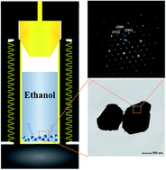
Single crystalline sub-micron Cu2ZnSnS4 (CZTS) powders were successfully synthesized by a facile solvothermal method, using L-cysteine as sulfur precursor. It was confirmed that pure kesterite structured CZTS powders were synthesized at 400 °C after 5 h, with the irregular polygonal particle size being 500 nm to 1 μm. Interestingly, single crystalline CZTS particles were also obtained by simple solvothermal treatment without post annealing. The H2S released from L-cysteine had an impact on the growth of CZTS particles at high temperature. Further, the as-synthesized CZTS powders were used as counter electrode for dye-sensitized solar cells (DSSCs) and it is indicated that the CZTS counter electrode based DSSCs show a conversion efficiency of 4.243%.


Kesterite-based thin film photovoltaic cells using Cu2ZnSnS4 (CZTS), Cu2ZnSnSe4 (CZTSe), and Cu2ZnSn(S,Se)4 (CZTSSe), respectively, as absorber layers are very promising for inexpensive photovoltaic electricity generation. This is due to the earth abundance and low-toxicity of the materials, their near-optimum direct band gap energy of 1.0–2.0 eV, high absorption coefficient (>104 cm−1), theoretical limit PCE of 32.2% and the rapid improvement in power conversion efficiency (more than 10%) from this family of compounds.1–3 Recently, many approaches have been developed to fabricate CZTS/CZTSSe thin films, such as vacuum based deposition (evaporation and sputtering), chemical vapor deposition, electrodeposition, and solution-based processing. As the vacuum based deposition methods suffer from relatively low throughput, low material utilization, stringent requirements of vacuum equipment, high temperature, and complicated operations, these costly methods will face many difficulties in large scale production. In this regard, various solution-based approaches have been developed owing to their advantages of low-cost and high throughput.4,5 Solution-based processing approaches can be further sub-divided into two kinds. They are based on whether the kesterite compound is formed before applying the liquid coating (as with many nanocrystal ink approaches) or the kesterite compound is formed only after applying liquid coating (as in hydrazine slurry based approaches and sol–gel molecular-ink approaches).6 Furthermore, as mentioned in many reports, it is easier to control the phase structure, particle size, homogeneity, and contents of the defects in the CZTS thin films, if the kesterite particles are formed before fabricating the liquid coating. Recently, the synthesis of CZTS particles involves hot-injection, microwave irradiation and hydrothermal/solvothermal method.7–12 However, as for hot-injection, most research interests focus on the fabrication of oil-soluble CZTS nanocrystals and some long, toxic organic ligands are used, which will deteriorate the performance of the solar cells. During these three years, a facile and green hydrothermal/solvothermal method was introduced to synthesize CZTS nanoparticles or microparticles, without using expensive, toxic and long-chain organic solvent. In a conventional hydrothermal/solvothermal synthesis, the ethylene glycol, or ethylenediamine were always used as solvent or stabilizer, and the reaction temperature was maintained ranged from 180–220 °C.13,14 However, the reported hydrothermal/solvothermal approach aims to obtain ultrafine nanometer scale CZTS, then the coating fabricated by screen printing, drop-casting, roll-to-roll or knife coating will be under sulfuration or other heat treatment, in order to increase the grain size (micron level) and crystallization, leading to the higher efficiency thin film solar cells. And there comes a problem like that, the melting point of CZTS is as high as 1000 °C but the sulfuration temperature can't be beyond 600 °C.15–18 Then, it is hard to fabricate the thin film of high quality and less grain boundaries through annealing nanometer scale CZTS crystals.

Thus, the idea of synthesizing the micron or sub-micron CZTS particles was proposed. In this paper, a facile solvothermal method was employed to synthesize the sub-micron CZTS powders, with the size ranging from 500 nm to 1 μm. The phase structure, morphology, crystal characteristics and optical property of the CZTS samples are investigated respectively by X-ray diffraction (XRD), Raman spectra (with 325 nm and 514 nm He–Ne laser employed as the excitation source respectively), transmission electron microscopy (TEM), field emission scanning electron microscopy (FE-SEM), energy dispersive X-ray spectroscopy (EDS), selected area electron diffraction (SAED) and UV-Vis absorption spectrophotometer (UV-Vis). The solvothermal parameters, such as reaction time, were adjusted to acquire the pure phase CZTS of kesterite-structure. Primary growth mechanism for the formation of single crystalline sub-micron CZTS samples is addressed.

CZTS single crystalline sub-micron powder was synthesized by high temperature solvothermal method. All reagents were of analytical grade and used without further purification. In a solvothermal process, Cupric(II) acetate monohydrate, zinc(II) acetate, stannic(IV) chloride and L-cysteine (Sinopharm Chemical Reagent Co., Ltd, China) were added into a stainless autoclave, which was filled with anhydrous ethanol (Sinopharm Chemical Reagent Co., Ltd, China) up to 70% of the total volume (50 mL) without stirring. The final concentrations of the Cu, Zn, Sn precursors were fixed at 1 mmol, 0.5 mmol, 0.5 mmol, and the S precursor (4 mmol) was kept higher than stoichiometric ratio for the complete sulfurization of the compound (as seen in Table 1). The autoclave was sealed and maintained at 400 °C for 1–48 h under autogenous pressure and then allowed to cool to room temperature naturally. During this process, Cu2+, Sn4+, Zn2+ cations and S2− anion were changed into CZTS phase through oxidation–reduction reactions. After cooling, the powders were centrifuged, washed with ethanol and the supernatant was discarded. Then the precipitation was baked at 80 °C in air overnight for characterization.

Table 1 The CZTS samples treated at 400 °C for different reaction time
Sample Temperature/oC Reaction time/h Cu[thin space (1/6-em)]:[thin space (1/6-em)]Zn[thin space (1/6-em)]:[thin space (1/6-em)]Sn[thin space (1/6-em)]:[thin space (1/6-em)]S/mmol
400-1 400 1 1[thin space (1/6-em)]:[thin space (1/6-em)]0.5[thin space (1/6-em)]:[thin space (1/6-em)]0.5[thin space (1/6-em)]:[thin space (1/6-em)]4
400-2 3
400-3 5
400-4 24
400-5 48


The phase characteristics of the products were determined by X-ray diffraction (XRD) and Raman spectra. The size, shape, composition and crystal structure of the obtained CZTS powders were investigated by transmission electron microscopy (TEM), field emission scanning electron microscopy (FE-SEM), energy dispersive X-ray spectroscopy (EDS) and from its selected area electron diffraction (SAED). The absorption spectra were recorded with a diffuse reflectance UV-Vis absorption spectrophotometer, which was equipped with an integrating sphere attachment. In typical measurements, CZTS inks were spin-coated on a glass, so as to obtain the CZTS film. The wavelength was ranged from 200 to 1100 nm.

The crystal structure of CZTS has two related tetragonal structures consisting of stannite and kesterite.1,2 Kesterite has a tetragonal unit cell, with sulfur atoms located in a face-centered-cubic sub-lattice. The Cu, Zn, and Sn atoms occupy half the tetrahedral interstitial sites within the S sub-lattice, with compositional order. Similar to chalcopyrite CIGS, kesterite CZTS exhibits diffraction peaks in addition to those observed from the compositionally disordered sphalerite compound, such as the (101) and (211) peaks. The phase development of the CZTS powders synthesized at 400 °C for different reaction time is shown in Fig. 1. The observed diffraction peaks indicate that kesterite-structure CZTS (CAS 26-0575) is obtained during solvothermal process. The three strong diffraction peaks around 28.5°, 47.3° and 56.2° are assigned to those crystal faces of (112), (220) and (312).19,20 However, when the reaction time is 1 h or 3 h, it is apparent that some undesired impurity phases appear in the XRD patterns, such as Cu2−xS and ZnS. The reason for the secondary sulphide formation was described by Regulacio.21 It is proposed that the formation of CZTS nanoparticles involves nucleation and growth. The copper sulfide initially forms and serves as the starting point for growth of CZTS, directly affecting the crystal structure of the generated CZTS.21 If the secondary sulphides have not reacted with each other completely, some impurity phases may remain. With the reaction time extension to 5 h, the sharper and higher diffraction peaks are obtained. In addition, some small diffraction peaks around 18.3°, 29.6°, 33.1°, 37.9°, 58.9° and 76.4° are observed in Fig. 1(c), which could be indexed to those crystal faces of (101), (103), (200), (211), (224) and (332). Thus, it is confirmed that the kesterite-structure CZTS phase is obtained through 5 h reaction and the high temperature solvothermal treatment is beneficial to significant improvement of crystallinity. However, if the reaction time is extended to 24 or 48 h, there are other characteristic peaks of impurities appearing, such as Cu4SnS6, Cu2−xS and ZnS, and the CZTS peaks nearly disappear. These impurity phases may derive from the CZTS phase resolving under the high temperature for longer time and it is consistent with the reports of Weber. They have declared that volatile SnS and S are lost from the sample at annealing a CZTS film in vacuum to 500 °C or higher for a long time.16,18 The proposed stoichiometric chemical equilibrium reaction is illustrated by eqn (1). On the basis of eqn (1) and the situation of this high temperature solvothermal treatment (400 °C), it is assumed that partial reduction of SnS would lead to the decomposition reaction and the other solid secondary phases are left.

 
Cu2ZnSnS4(s) ↔ Cu2S(s) + ZnS(s) + SnS(g) + 1/2S2(g) (1)


image file: c4ra12815j-f1.tif
Fig. 1 Schematic illustration of the synthetic route of single crystalline sub-micron CZTS powders (a), XRD patterns for the as-synthesized CZTS powders for different reaction time (b), XRD pattern and Raman spectra for the CZTS powders formed at 400 °C for 5 h (c) and (d), with the 514 nm He–Ne laser as excitation source.

Furthermore, it is noteworthy that the XRD profiles of tetragonal Cu2SnS3 (CAS 89-4714) and cubic ZnS (CAS 80-0020) are similar to that of CZTS phase as shown in Fig. 1(c). Therefore, the further structural information of the sample on macroscopic scale is obtained from Raman spectrum (as shown in Fig. 1(d)). The peaks from Cu2SnS3 (352 cm−1), ZnS (346 cm−1), and Cu2−xS (475 cm−1) phases are not observed. The Raman peak at 340 cm−1, 290 cm−1 is from kesterite CZTS and the biggest peak is known to be positioned at 339 cm−1. Furthermore, a minor peak for CZTS (373 cm−1) also appears, if 325 nm excitation source was used (as seen in Fig. S2). These results exclude the presence of other binary or ternary compounds, with only CZTS existing, which are similar to those in previous reports.13,22–24

As be seen in Fig. 2(a) and (b), the size of CZTS powders with irregular polygonal shape is mostly falling in the range of 500–1000 nm. It is definitely confirmed that the sub-micron CZTS powders were successfully synthesized at 400 °C for 5 h. Interestingly, the clear presence of sharp diffraction spots in Fig. 2(c) indicates that the CZTS particles are highly crystallized and proved to be single crystalline. Furthermore, the diffraction spots are indexed as (112), (200) and (101) respectively, which is consistent with the above XRD data. The atomic ratio of Cu[thin space (1/6-em)]:[thin space (1/6-em)]Zn[thin space (1/6-em)]:[thin space (1/6-em)]Sn[thin space (1/6-em)]:[thin space (1/6-em)]S was found to be 23.27[thin space (1/6-em)]:[thin space (1/6-em)]12.59[thin space (1/6-em)]:[thin space (1/6-em)]13.58[thin space (1/6-em)]:[thin space (1/6-em)]50.56, which is close to the stoichiometric value of 2[thin space (1/6-em)]:[thin space (1/6-em)]1[thin space (1/6-em)]:[thin space (1/6-em)]1[thin space (1/6-em)]:[thin space (1/6-em)]4 (as seen in Table S1). The formation mechanism of single crystalline sub-micron CZTS is explained as follows. The L-cysteine could play important roles from three aspects in this solvothermal method. Firstly, it acts as a complexing reagent by forming metal–cysteine ligands, and secondly it acts as the source of sulfur by breaking the C–S bond. After the reactant dissolving, metal ions are complexed with L-cysteine to form the precursors. The formation mechanisms can be explained in eqn (2).25 The partial Cu2+ is reduced to Cu+ by L-cysteine solution at solvothermal process. Then, the Sn2+ could be slowly oxidized to Sn4+ by Cu+. Finally, the complexes of [Cu(L-cysteine)n]+, [Zn(L-cysteine)n]2+, [Sn(L-cysteine)n]4+ are obtained through the chelation between metal cation and cysteine ligand. The metal–cysteine ligands serve as a reservoir of metal ions and regulate the nucleation rate by the slow release of ions into solution. When the reactants are heated, the released S2− from the L-cysteine combines with the metal ions and precipitation of sulfides (Cu2−xS, ZnS or CZTS) occurs owing to the stronger coordination capability between metal ions and S2−. Consequently, the initial CZTS crystal nucleus is obtained.

Cu2+ → Cu+, 2Cu2+ + Sn2+ → 2Cu+ + Sn4+

Cu+ + nL-cysteine → [Cu(L-cysteine)n]+

Sn4+ + nL-cysteine → [Sn(L-cysteine)n]4+

Zn2+ + nL-cysteine → [Zn(L-cysteine)n]2+
 
[Cu(L-cysteine)n]+ + [Sn(L-cysteine)n]4+ + [Zn(L-cysteine)n]2+ → Cu2ZnSnS4 (2)


image file: c4ra12815j-f2.tif
Fig. 2 Bright-field TEM images (a) and (b), SAED pattern (d) for single crystalline sub-micron CZTS powders synthesized for 5 h and the picture of well-dispersed CZTS/ethanol inks (d).

Thirdly, it is reported that the L-cysteine could act as reductant by releasing hydrogen sulfide (H2S) during solvothermal reaction.25–27 Among the solution-based processing approaches, an additional annealing step is mandatory to improve the crystallinity and grain size of CZTS particles in the as-prepared thin films. The heat treatment is always performed in a small graphite box in an excess sulfur or H2S atmosphere at a temperature ranged from 400 °C to 600 °C.18 During this solvothermal process, it is equivalent to treat the CZTS crystal nucleus with H2S annealing at 400 °C, as the high temperature is employed. Thus, the crystallinity of CZTS samples is greatly improved, which is consistent with the results of XRD patterns. Furthermore, the growth rate is faster than the nucleation rate, as the excess forming H2S and high temperature are provided in the autoclave. And the single crystalline sub-micron CZTS powders are obtained during the solvothermal method. In addition, Fig. 2(d) shows the picture of well-dispersed CZTS/ethanol inks solution. The fabrication of well-dispersed and stable inks is the most important step to fabricate ink-based solar cells.

The optical band gap can be calculated by using the intercept method and the following formula:9

 
(αhν)n = A(Eg) (3)
where α is the absorption coefficient near the absorption edge, A is a constant and n characterizes the transition process. Here n = 2 and 1/2 stands for the direct band gap and indirect band gap, respectively. The CZTS is a direct band gap semiconductor. Fig. 3 shows the optical band gap calculated using eqn (3). The band gap is approximated to be 1.45 eV by plotting (αhν)2 versus the energy and extrapolating the linear part of the spectrum, (αhν)2 = f(), to zero. This value is in the optimal band gap window for the absorber of solar cells.10,28


image file: c4ra12815j-f3.tif
Fig. 3 Plot of (αhν)2 vs. photon energy () of the as-synthesized CZTS powders at 5 h.

The device performance was measured using Pt/FTO and CZTS/FTO counter electrodes and N719-TiO2/FTO working electrode separately. Fig. 4 shows the JV characteristics of DSSCs under 100 mW cm−2 illumination. The parameters for standard Pt/FTO counter electrodes based DSSCs device is as follows: short circuit current density (JSC) of 9.861 mA cm−2, open circuit voltage (VOC) of 0.774 V, fill factor (FF) of 44.674%, and efficiency (η) of 3.412%. Replacing the Pt-coated FTO with the CZTS-5 film counter electrodes, the parameters of the cell change significantly. The FF increases significantly from 44.674% to 60.968% (36% increase), and the η also improves from 3.412% to 4.243% (24% increase). However, the VOC and JSC decrease slightly up to 0.746 V and 9.318 mA cm−2 respectively.


image file: c4ra12815j-f4.tif
Fig. 4 Current–voltage characteristics of the dye-sensitized solar cells (DSSCs). The inset shows the JSC, VOC, FF, η, and structure of the solar cells.

A simple and relatively convenient solvothermal synthesis of the single crystalline sub-micron Cu2ZnSnS4 (CZTS) powders is proposed. The irregular polygonal sub-micron particles, with diameters in the range of 500 nm to 1 μm, are obtained without using any post high temperature annealing. The highly crystalline nature of the CZTS samples was confirmed by the XRD. Furthermore, it is implied that partial reduction of volatile SnS or S would lead to the decomposition of CZTS at solvothermal treatment for longer time and the other impurity phases are left. Interestingly, a single crystalline CZTS particle was observed from selected area electron diffraction pattern and it was well consistent with the XRD results. The role of L-cysteine and high temperature (400 °C) in the solvothermal reaction is clarified and it is believed that the H2S released from the L-cysteine leads to the formation of single crystalline sub-micron CZTS particles. Finally, the fabricated CZTS/FTO counter electrode based DSSCs has an enhanced fill factor (36%) and increased efficiency (24%) compared with traditional DSSCs using Pt as the counter electrode.

Acknowledgements

This work was supported by the National Nature Science Foundation of China (Grant no. 51202112).

Notes and references

  1. D. B. Mitzi, O. Gunawan, T. K. Todorov, K. Wang and S. Guha, Sol. Energy Mater. Sol. Cells, 2011, 95, 1421–1436 CrossRef CAS PubMed.
  2. D. A. R. Barkhouse, O. Gunawan, T. Gokmen, T. K. Todorov and D. B. Mitzi, Prog. Photovoltaics, 2012, 20, 6–11 CAS.
  3. H. Katagiri, K. Jimbo, W. S. Maw, K. Oishi, M. Yamazaki, H. Araki and A. Takeuchi, Thin Solid Films, 2009, 517, 2455–2460 CrossRef CAS PubMed.
  4. B. Shin, O. Gunawan, Y. Zhu, N. A. Bojarczuk, S. J. Chey and S. Guha, Prog. Photovoltaics, 2013, 21, 72–76 CAS.
  5. N. Yu, R. Zhong, W. Zhong, X. Chen, J. Luo, X. Gu, X. Hu, L. Zhang, J. Hu and Z. Chen, RSC Adv., 2014, 4, 36046–36052 RSC.
  6. H. Xin, J. K. Katahara, I. L. Braly and H. W. Hillhouse, Adv. Energy Mater., 2014, 4, 1301823 CrossRef.
  7. S. N. Park, S. J. Sung, D. H. Son, D. H. Kim, M. Gansukh, H. Cheong and J. K. Kang, RSC Adv., 2014, 4, 9118–9125 RSC.
  8. Q. Guo, H. W. Hillhouse and R. Agrawal, J. Am. Chem. Soc., 2009, 131, 11672–11673 CrossRef CAS PubMed.
  9. Y. Gao, H. Yang, Y. Zhang, J. Li, H. Zhao, J. Feng, J. Sun and Z. Zheng, RSC Adv., 2014, 4, 17667–17670 RSC.
  10. C. Steinhagen, M. G. Panthani, V. Akhavan, B. Goodfellow, B. Koo and B. A. Korgel, J. Am. Chem. Soc., 2009, 131, 12554–12555 CrossRef CAS PubMed.
  11. A. Khare, A. W. Wills, L. M. Ammerman, D. J. Norris and E. S. Aydil, Chem. Commun., 2011, 47, 11721–11723 RSC.
  12. Y. Xie, C. Zhang, F. Yue, Y. Zhang, Y. Shi and T. Ma, RSC Adv., 2013, 3, 23264–23268 RSC.
  13. Y. L. Zhou, W. H. Zhou, M. Li, Y. F. Du and S. X. Wu, J. Phys. Chem. C, 2011, 115, 19632–19639 CAS.
  14. W. Liu, B. Guo, C. Mak, A. Li, X. Wu and F. Zhang, Thin Solid Films, 2013, 535, 39–43 CrossRef CAS PubMed.
  15. Q. Guo, G. M. Ford, W. C. Yang, B. C. Walker, E. A. Stach, H. W. Hillhouse and R. Agrawal, J. Am. Chem. Soc., 2010, 132, 17384–17386 CrossRef CAS PubMed.
  16. A. Weber, R. Mainz and H. W. Schock, J. Appl. Phys., 2010, 107, 013516 CrossRef PubMed.
  17. A. Redinger and S. Siebentritt, Appl. Phys. Lett., 2010, 97, 1–3 CrossRef PubMed.
  18. A. Redinger, D. M. Berg, P. J. Dale and S. Siebentritt, J. Am. Chem. Soc., 2011, 133, 3320–3323 CrossRef CAS PubMed.
  19. Y. L. Zhou, W. H. Zhou, Y. F. Du, M. Li and S. X. Wu, Mater. Lett., 2011, 65, 1535–1537 CrossRef CAS PubMed.
  20. W. C. Liu, B. L. Guo, X. S. Wu, F. M. Zhang, C. L. Mak and K. H. Wong, J. Mater. Chem. A, 2013, 1, 3182–3186 CAS.
  21. M. D. Regulacio, C. Ye, S. H. Lim, M. Bosman, E. Ye, S. Chen, Q. H. Xu and M. Y. Han, Chem.–Eur. J., 2012, 18, 3127–3131 CrossRef CAS PubMed.
  22. C. Zou, L. Zhang, D. Lin, Y. Yang, Q. Li, X. Xu, X. Chen and S. Huang, CrystEngComm, 2011, 13, 3310–3313 RSC.
  23. P. A. Fernandes, P. M. P. Salome and A. F. da Cunha, Thin Solid Films, 2009, 517, 2519–2523 CrossRef CAS PubMed.
  24. A. J. Cheng, M. Manno, A. Khare, C. Leighton, S. A. Capmbell and E. S. Aydil, J. Vac. Sci. Technol., A, 2011, 29, 051203 Search PubMed.
  25. Q. Cai, X. J. Liang, J. S. Zhong, J. S. Zhong, M. G. Shao, Y. Wang, X. W. Zhao and W. D. Xiang, Acta Phys.-Chim. Sin., 2011, 27, 2920–2926 CAS.
  26. Y. Xia, Z. Chen, Z. Zhang, X. Fang and G. Liang, Nanoscale Res. Lett., 2014, 9, 1–7 CrossRef CAS PubMed.
  27. Z. Zhang, C. Zhou, L. Huang, X. Wang, Y. Qu, Y. Lai and J. Li, Electrochim. Acta, 2013, 114, 88–94 CrossRef CAS PubMed.
  28. C. Wang, C. Cheng, Y. Cao, W. Fang, L. Zhao and X. Xu, Jpn. J. Appl. Phys., 2011, 50, 5003 Search PubMed.

Footnote

Electronic supplementary information (ESI) available. See DOI: 10.1039/c4ra12815j

This journal is © The Royal Society of Chemistry 2015
Click here to see how this site uses Cookies. View our privacy policy here.