Seung Jin Chaeab,
Yong Hwan Kimab,
Tae Hoon Seoc,
Dinh Loc Duongab,
Seung Mi Leed,
Min Ho Parke,
Eun Sung Kimab,
Jung Jun Baeab,
Si Young Leeab,
Hyun Jeonga,
Eun-Kyung Suhc,
Cheol Woong Yange,
Mun Seok Jeong*ab and
Young Hee Lee*ab
aCenter for Integrated Nanostructure Physics, Institute for Basic Science, Sungkyunkwan University, Suwon 440-746, Republic of Korea. E-mail: leeyoung@skku.edu; mjeong@skku.edu
bDepartment of Energy Science, Department of Physics, Sungkyunkwan University, Suwon 440-746, Republic of Korea
cSchool of Semiconductor and Chemical Engineering, Chonbuk National University, Jeonju 561-756, Republic of Korea
dCenter for Nanocharacterization, Korea Research Institute of Standards and Science, Daejeon 305-340, Korea
eDepartment of Advanced Materials Engineering, Sungkyunkwan University, Suwon 440-746, Korea
First published on 27th November 2014
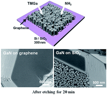
We report high-quality GaN crystals grown directly on graphene layers without a buffer layer by metal–organic chemical vapour deposition. Photoluminescence and Raman spectra revealed that GaN crystals grown on graphene layers had mild strain as compared to those grown on sapphire and SiO2 substrates. Etch pits were not observed on the surface of GaN/graphene, in which threading dislocations were diminished inside the bulk. This is markedly different from GaN/sapphire, in which threading dislocations were present on GaN surfaces. This opens a new possibility that graphene with π electrons and hexagonal symmetry could be an ideal substrate for GaN crystal growth instead of expensive sapphire substrates.
Graphene is a layered structure of hexagonally arranged carbon atoms with strong σ bonds within the plane, whereas weak π electrons are exposed to the surface. Thus, the interaction of graphene with other materials is generally weak. For example, if GaN is grown on a graphene substrate, the lattice mismatch may be very different from that of GaN grown on sapphire, which may reduce the dislocation density or generate different types of dislocations. Ideally, the strain energy could be reduced owing to the weak interaction between graphene and the host material. Therefore, graphene could act as an ideal substrate for the crystal growth of numerous materials.6–10 In this report, we demonstrate this concept by introducing graphene as a substrate for direct growth of GaN instead of sapphire. Highly crystalline GaN (0001) on a graphene substrate was synthesized by metal–organic chemical vapour deposition (MOCVD) without using a buffer layer. No yellow band in the photoluminescence (PL) spectra was observed. Tensile stress accumulated on the GaN/graphene, but its magnitude was smaller than that of GaN/sapphire. Unlike GaN/sapphire, which shows threading dislocations on the GaN surface, etch pits were not observed on the surface of the GaN/graphene, where the threading dislocations were diminished inside the bulk material.
Fig. 2a shows the photoluminescence (PL) spectra at room temperature of the grown GaN samples. GaN grown on the graphene (Gr)/SiO2/Si and Gr/sapphire substrates showed clear excitonic PL peaks at 3.38 and 3.39 eV, respectively, without a yellow luminescence band. This is similar to the GaN grown on sapphire except for a slight peak shift from 3.42 eV, but it is in contrast with GaN grown on the SiO2/Si substrate, in which a yellow luminescence (YL) band was observed at approximately 2.2 eV (band width ∼1 eV), representing defect formation in the GaN film. The values for the full width at half maximum of the excitonic PL peaks for the three substrates were similar to each other, indicating that GaN crystallites grown on graphene have a crystal quality similar to that of GaN grown on sapphire. The respective red shifts of 0.03 and 0.04 eV for the GaN grown on the Gr/SiO2/Si and Gr/sapphire substrates as compared to GaN grown on sapphire could be related to strain relaxation, which will be discussed later.
The presence of residual stress of the GaN film is well represented by the frequency shift and width of the E2 high (EH2) mode.14–18 Fig. 2b shows clear EH2 and A1 LO modes for the four samples at room temperature. The EH2 mode of strain-free GaN is 567 cm−1 (see Table 1). The GaN film grown on the sapphire substrate induces general compressive strain, whereas the GaN film on the silicon substrate induces tensile strain.19 In Fig. 2b, the blue shift of the EH2 peak frequency by 7.2 cm−1 for the GaN directly grown on sapphire and by 2.7 cm−1 for the GaN grown on the Gr/sapphire substrate corresponds to compressive strain, although the latter is milder than the former. This indicates that the strain is minimized by using graphene as a substrate. On the other hand, the red shift by 1.8 cm−1 in the GaN grown on the Gr/SiO2/Si and SiO2/Si substrates is an indication of mild tensile stress. This implies that the graphene transferred onto different substrates is slightly influenced by the substrate type, presumably owing to the surface morphology of the substrate.
Substrate | Equip. | Raman (EH2) | PL (eV) | Thickness (μm) | Threading dislocation density (cm−2) | Stress | Nucleation layer | |
---|---|---|---|---|---|---|---|---|
Ref. 14 | — | HVPE | 567 | 50 | 3 × 10⁶ | — | — | |
Ref. 15 | Sapphire | HVPE | 569.1 | 3.42 | 80 | <108 | — | — |
Ref. 16 | Si (111) | MOCVD | 565.2 | 3.405 | 1.5, 2.5 (ref. 24) | −108 (ref. 24) | Tensile | Gan/AIN |
Ref. 17 | 6H–SiC | MBE | 565.3 | 3.414 | 2–5 | 4 × 10⁸ (ref. 21) | Tensile | AIN |
Ref. 18 | Sapphire | MOCVD | 568.5 | 3.432 | 2–5 | — | Compressive | — |
This work | Graphene/SiO2/Si | MOCVD | 565.2 | 3.38 | 10 | ![]() |
Tensile | GaN |
Fig. 2c and d show the PL spectra of GaN on sapphire and on Gr/sapphire as a function of temperature from 10 K to 300 K. The spectra are dominated by neutral donor–bound recombination.20 Red shifts and broadening of all emission lines were observed as the temperature decreased. The temperature dependence of the line width is attributed to phonon-induced band broadening.21 The characteristic red shift with increasing temperature is attributed to band gap reduction from lattice expansion and to electron–phonon interaction.22 As shown in Fig. 2c, no donor–acceptor pairs (DAP) were observed in GaN grown on sapphire. On the other hand, DAP lines were clearly visible in the GaN grown on Gr/sapphire. As shown in Table 2, the gaps between DAP, DAP-1LO, and DAP-2LO are nearly regulated with an interval of ∼100 meV in the GaN grown on Gr/sapphire. Carbon could be a source of acceptor sites owing to the presumably disassembled graphene layers during nucleation of GaN by pyrolysis at high growth temperatures. Carbon doping in GaN crystals is generally obtained by implantation or by using CBr4 gas.23,24 In these methods, defects in GaN crystals are generated by physical force and etching, resulting in the appearance of a YL band. In the current case of Gr/sapphire, the carbon atoms were doped naturally by pyrolysis, without creating defect sites by physical damage.
The mild tensile stress in GaN grown on Gr/SiO2/Si is markedly different from the high compressive stress accumulated in GaN grown on Gr/sapphire. Fig. 3 shows the theoretical simulation data based on density functional theory, which is generally used in nanostructure calculations.25 Fig. 3a shows the ball-and-stick atomic structure of the GaN monolayer. The Ga–Ga or N–N distance is 3.18 Å. This closely matches the separation distance (3.23 Å) of the next bond-centre site of graphene, as shown in Fig. 3b. Every Ga and N atom is positioned at the bond-centre site of graphene. Overlapping a super cell of GaN on the graphene layer resulted in an alternative location of N atoms at every other top site of graphene (indicated by green dashed line) and Ga atoms alternatively at H (hexagonal) sites and bond-centre sites of graphene (red dashed line) (see Fig. 3c). As the number of Ga and N atoms increases to form a monolayer, the GaN structure is converted into a hexagonal phase. The Ga–N bond length approaches that of the bulk material, as shown in Fig. 3d, as the number of layers increases. Maintaining hexagonal symmetry and minimum strain as compared to hexagonal GaN/sapphire is an advantage of using graphene as a substrate. The graphene layer could be strained by the substrate, which is evidenced by the difference in the binding energy with and without relaxation of the graphene layer. On the other hand, the interfacial binding energy increases, becoming saturated to less than −3.0 eV per GaN at six GaN layers. This is the origin of stress of the grown GaN, even with a graphene substrate. At high growth temperatures, therefore, the grown GaN layers, in particular those near the interface, are expected to be slightly strained. Nevertheless, this interfacial energy is smaller than that of GaN/sapphire, as shown in the calculated strain, stress, and frequency shift in Table 3. As a consequence, we expect the strain developed on the graphene surface to be presumably smaller that on sapphire from the theoretical simulation data.
GaN on Gr/SiO2/Si | GaN on sapphire | GaN on Gr/sapphire | |
---|---|---|---|
a Δω (cm−1) = Cσxx, Δω: EH2 phonon frequency, C: linear stress coefficient (cm−1 per GPa) → 2.56 cm−1 per GPa, σxx: biaxial stress (GPa) bulk GaN → 567 cm−1, E = stress/strain = σ/ε, E: Young's modulus of bulk GaN → 160–290 GPa. | |||
Δω (cm−1) | −1.8 | +7.2 | +2.7 |
σxx (GPa) | −0.7 | +2.8 | +1.1 |
ε (%) | 0.2–0.4 | 0.9–1.8 | 0.4–0.6 |
As shown in Table 3, using the phonon frequency (EH2) change with respect to the bulk value (567 cm−1),14 Δω (cm−1) = Cσxx formula,26 already well known relationship to calculate the strain of GaN grown on sapphire and that of GaN grown on Gr/sapphire simultaneously, the biaxial stress (σxx) was extracted. The linear stress coefficient, C, is a constant value. Young's modulus (E = σ/ε) was used to obtain the strain value by substituting the value of the obtained stress. The mild tensile stress on GaN/Gr/SiO2/Si was expected owing to the weak interaction between graphene and GaN. The strain of GaN/Gr/sapphire is approximately three times smaller than that of GaN/sapphire, as expected from the theoretical arguments given in the previous paragraph.
Fig. 4a shows the cross-sectional transmission electron microscope (TEM) images of GaN near the interface of graphene. The inset image clearly shows no defects such as voids or cracks. Multilayer (∼10 layers) graphene with slight variations in thickness, which is a characteristic of multilayer graphene on a Ni substrate,11 was also clearly visible at the interface. In addition, the high-resolution TEM image of GaN crystals in Fig. 4b indicates a well-aligned crystal lattice array. The lattice spacing between the nearby planes is 0.52 nm, in good agreement with the d-spacing of GaN (0001) planes grown on sapphire.13 The electron diffraction pattern shows a (110) zone axis pattern of the grown GaN crystal on graphene in Fig. 4c (see also ESI, Fig. S3†).
GaN epitaxial layers can be grown, in general, by the well-known two-step MOCVD method on (0001) sapphire.27 These layers contain a high density of threading dislocations (TDs). There are three types of TDs in GaN: pure edge, pure screw, and mixed types. Epitaxial layers predominantly contain pure edge-type TDs that have a line direction perpendicular to the GaN sapphire interface. As a consequence, edge TDs are generated as a result of the large lattice mismatch between GaN and sapphire. TDs are detrimental to electronic and photoelectronic devices. The TD density is, therefore, a critical parameter for judging the quality of GaN films. To understand the formation of TDs in GaN grown on Gr/SiO2/Si, we inspected two TEM cross-sectional micrographs. It is commonly presumed that TDs evolve from the coalescence of tilted and twisted islands during the initial stages of GaN deposition.28 Bright-field TEM images, recorded under two-beam conditions in order to image all dislocations with different Burgers vectors, were used to estimate the density. Fig. 5a and b show the cross-sectional TEM images of the sample grown on the Gr/SiO2/Si substrate. The TD types in the GaN crystal were determined by applying the g·b criterion to the two-beam images of the cross-sectional TEM specimen (g is a reciprocal lattice vector and b is a Burgers vector), which were recorded near the [110] zone axis with g = [1
00] in Fig. 5a and b.29
Here we discuss pure edge dislocations in more detail. The dislocations shown only in g = [100] of the two-beam image are pure edge dislocations because threading dislocations have a dislocation line vector parallel to the c-axis, as shown in Fig. 5b. On the other hand, the dislocations shown in the [11
0] zone axis of the two-beam image are pure edge, pure screw, and mixed dislocations, as shown in Fig. 5a. This indicates that the predominant dislocations in GaN crystals grown on Gr/SiO2/Si were screw- and mixed-type dislocations. The numbers of edge-, screw-, and mixed-type dislocations for GaN crystals grown on Gr/SiO2/Si differed from those of previous studies on sapphire substrates, which revealed pure edge-type dislocations only.30–33 The predominance of mixed-type dislocations on Gr/SiO2/Si may be attributed to a higher density of screw-type dislocations as compared to those on GaN on sapphire. The dashed line in Fig. 5b is the grain boundary of the GaN crystal. The number of TDs was counted at random positions on a scale of 2 μm. The estimated total TD density ranged from 8 × 108 cm−2 to 3.6 × 109 cm−2, which is comparable to that of GaN grown on sapphire, 6H–SiC, and Si(111) but slightly higher than that of GaN grown on sapphire substrates (see Table 1).
Convergent beam electron diffraction (CBED) is one of the most powerful techniques for determining the polarity of GaN crystals on graphene.34 Since GaN is a non-centrosymmetric crystal, JEMS software was used to simulate the index of (0002) and (000) directions of the experimental patterns and consequently to deduce the nanostructure polarity (Fig. 5c and d). The intensity distribution change also depends on the sample thickness. The simulation and experimental disks agreed well with each other, indicating that these crystals were grown with Ga polarity.
Unlike typical GaN crystals grown on sapphire, GaN grown on Gr/SiO2/Si in the current study generated edge dislocations perpendicular to the (0001) growth direction, and therefore most dislocations were buried within the GaN crystals. Thus surface etch pits were not visible on the surface of GaN grown on Gr/SiO2/Si (Fig. 6a). Even after surface etching with 0.5 mol KOH at 80 °C for 20 min, etch pits were not visible, as shown in the two side images of Fig. 6a. On the other hand, for GaN/SiO2/Si, several large etch pits and many small etch pits were formed, as shown in Fig. 6b. An etch pit density (EPD) of approximately 8 × 109 cm−2 was obtained, which is similar to the EPD of GaN grown on the sapphire substrate. The shape of the etch pits in the top view was clearly different from that of the side view, which shows cylindrical protrusions. Most dislocations were generated perpendicular to the growth direction. To demonstrate the quality of GaN crystals grown on graphene, we fabricated an light emitting diode (LED) using five-period InGaN/GaN multi-quantum wells (MQWs) (see ESI, Fig. S4†). Light emission was demonstrated from the as-fabricated LED. This opens the possibility of fabricating flexible LEDs in the near future.
![]() | ||
Fig. 6 FESEM images of GaN grown on (a) Gr/SiO2/Si and (b) SiO2/Si after etching for 20 min in 0.5 mol KOH. The right images show top and side views of GaN after etching. |
Footnote |
† Electronic supplementary information (ESI) available. See DOI: 10.1039/c4ra12557f |
This journal is © The Royal Society of Chemistry 2015 |