Yanwei Shena,
Xiaoqin Yan*a,
Zhiming Baia,
Xin Zhenga,
Yihui Suna,
Yichong Liub,
Pei Linb,
Xiang Chena and
Yue Zhang*ab
aState Key Laboratory for Advanced Metals and Materials, School of Materials Science and Engineering, University of Science and Technology Beijing, 100083, Beijing, PR China. E-mail: xqyan@mater.ustb.edu.cn
bKey Laboratory of New Energy Materials and Technologies, University of Science and Technology Beijing, 100083, Beijing, PR China. E-mail: yuezhang@ustb.edu.cn
First published on 15th December 2014
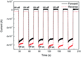
We report fabrication of an all inorganic, self-powered and rapid-response ultraviolet (UV) photodetector using solution-processed p-NiO/ZnO-nanorod array heterojunction. The device exhibited a fast binary-response with a rise time of 0.23 s and decay time of 0.21 s. A large responsivity of 0.44 mA W−1 was achieved for a 0.4 mW cm−2 UV light irradiation at a zero-bias voltage. The self-powered performance could be attributed to the proper built-in electric field between ZnO and NiO arising from the well-aligned energy-band structure of the device, which gives rise to a photovoltaic effect.
Recently zinc oxide (ZnO), especially nanostructured ZnO, has drawn more and more attention for its promising applications in photodetectors,4,13–17 light emitting diodes,18–20 solar cells,21–23 strain sensors,24,25 nanogenerators26–28 and field effect transistors,29,30 which benefits from its unique physical properties, such as wide bandgap (≈3.37 eV), high exciton binding energy (≈60 meV), high carrier mobility (>100 cm2 V−1 s−1 at RT), and high resistance to irradiation. Among all the ZnO nanostructures, one-dimensional nanorods are usually chosen to construct UV detectors due to their high crystallinity, high surface-to-volume ratio and excellent carrier transport property.14,31
Photoconductive detectors fabricated using composites of ZnO nanowires and other nanomaterials32,33 have been demonstrated to have enhanced photoresponse performance with the advantages of tunable spectral selectivity and fast response speed, but these devices usually need external power sources. According to the interface features, self-powered photodetectors typically have two structures, i.e. Schottky junction type and p–n junction type. Compared with the ZnO-based Schottky junction UV detectors, ZnO-based p–n junction UV detectors are more suitable for self-powered photodetectors due to their lower applied fields and faster response times.9 So far, several groups have reported the work on self-powered photodetectors based on ZnO based p–n junction. Onkar Game and co-workers reported a self-powered organic–inorganic hybrid photodetector comprising of n-type ZnO nanorods and p-type spiro-MeOTAD, which exhibited a high sensitivity (102) and a UV-visible rejection ratio of 300. The response time of τrise and τdecay were reported to be 200 μs and 950 μs, respectively.8 However, for organic–inorganic hybrid photodetectors, poor stability is a big challenge since the organic materials are quite sensitive to oxygen and humidity. Ni et al. demonstrated a self-powered spectrum-selective ZnO/NiO core–shell nanowire array photodetector that gave a high responsivity of ∼0.493 mA W−1 at a zero bias. Expensive high-vacuum MOCVD and RF magnetron sputtering equipment were utilized to grow the core ZnO nanowires and NiO shell layer respectively.10 A self-powered visible-blind UV detector with a fast response of rise time (≈20 μs) and decay time (≈219 μs) was constructed using a single n-type ZnO and a p-type GaN film by Bie et al.5 It is known to all that single ZnO nanowire based devices are usually just prototype devices because the nanowires are difficult to manipulate and easy to damage. Therefore, a lower-cost, stable and self-powered UV photodetector with rapid and remarkable photoresponse has to be studied further.
Here, we fabricated a p-NiO/ZnO-nanorod array based UV detector using an all solution-process method and studied its self-powered detection performance under a nominal zero bias. The structural properties, photoelectric response properties, and the self-powered mechanism of the devices were investigated in this study.
The morphologies of the ZnO nanorod array and NiO film were characterized using a Field emission scanning electron microscope (FESEM, FEI Quanta 3D). The crystalline and structural properties of the layers were investigated by X-ray diffraction (XRD) (Rigaku DMAX-RB with Cu Kα radiation l = 0.15406 nm) and confocal Raman microscopy (JY-HR800). UV-vis absorption spectra of the NiO films were measured using a UV-vis-NIR spectrometer (Varian Cary 5000). The photoelectric properties of the obtained UV photodetectors were characterized using a Semiconductor Characterization System (Keithley 4200). The UV light source was a 355 nm laser with a power of 20 mW.
![]() | ||
Fig. 2 The cross-sectional (a), top view (b) SEM morphologies of the p-NiO/n-ZnO nanorod array, and top view (c) SEM morphology of NiO film. |
As shown in Fig. 3a and b, the XRD patterns and Raman spectra of the p-NiO/n-ZnO nanorod array confirm the high quality of ZnO nanorod array and the existence of NiO. It can be observed from Fig. 3a that a dominant and intense (002) peak at 34.36° of ZnO showed that the grown ZnO was highly crystalline and well c-axis oriented, which is in line with the result of SEM morphologies. Only a weak (200) peak at 42.9° of NiO can be observed, which may be ascribed to the thin thickness. In order to further demonstrate the presence of NiO, Raman analysis was conducted. Fig. 3b shows two peaks of NiO at around 548.2 cm−1 and 1098.7 cm−1, which may be closely related to the oscillation of Ni–O in NiO. At the same time, the two peaks had a slight shift with respect to pure NiO, which was caused by the interaction between NiO and ZnO. The bandgap of NiO can be determined to be 3.55 eV from the plot of (αhν)2 vs. hν (α and hν are the absorption coefficient and photon energy, respectively), as indicated in the inset of Fig. 3c.
![]() | ||
Fig. 3 XRD patterns (a) and Raman spectra (b) of the p-NiO/n-ZnO nanorod array; (c) optical absorption spectrum of the NiO films and the inset shows a plot of (αhν)2 vs. hν. |
Fig. 4a represents the typical I–V characteristics of the device under dark and illumination by a 355 nm UV light with intensity of 3.2 mW cm−2, which showed a large rectification ratio (about 160 at ±3 V) and small leakage current (about 1.13 × 10⁻⁶ A at −3 V). The inset of Fig. 4a is the I–V curve under dark and illumination plotted on the semi-logarithmic scale. The ratio of photocurrent to dark current is about 102 when the device is reverse biased. At a very low forward voltage for V < 0.2 V, the dark current increases linearly with the voltage (I ∼ V), which demonstrates a transport mechanism following the Ohmic law. When V > 0.2 V, the dark current increases exponentially following the equation, I ∼ exp(αV), indicating a recombination-tunnelling mechanism usually observed in the wide bandgap p–n diodes.16,38 The constant α was evaluated to be 4.37 V−1. The bigger α than that of idea vacuum diode (1.5) indicates that more donor-like defects such as oxygen vacancies existed in the junction area than those in ZnO nanorod array epitaxial layer, providing the recombination-tunnelling path.39 These defects may decrease the width of depletion layer to a certain extent, thus suppressing the separation of photogenerated electron–hole pairs. It can be seen from Fig. 4b, an enlarged curve of Fig. 4a, that a measurable photovoltaic effect existed under UV illumination, which was responsible for the self-powered performance of the fabricated ZnO/NiO UV detectors. Specifically, a proper built-in electric field between ZnO and NiO arising from the devices' well-aligned energy-band structure (see Fig. 4c) could separate efficiently the photogenerated electron–hole pairs in ZnO at the heterojunction interface and help the charge carriers transport to corresponding electrodes, resulting in photocurrent.
The photocurrent response properties and stability of the ZnO/NiO based UV detectors was further investigated as shown in Fig. 5. The devices' photocurrent response plot was recorded at a nominal zero set bias under on/off switching radiation of 3.2 mW cm−2 UV light with an on/off internal of 15 s. Six repeat cycles were measured under a small forward and reverse bias of ≈0.1 mV. It can be seen from Fig. 5a that the photocurrent response was fast, consistent and repeatable. It should be noted that, under forward bias, the photocurrent alternated between positive and negative at the moment of switching the UV light on and off, which demonstrated an on/off binary-response arising from the photovoltaic behavior and low turn-on voltage of the ZnO/NiO device. The photosensitivity of this binary-response device for UV detection exceeded the value of ∼105 previously reported. Similar results could also be found in the ZnO/CuSCN based UV detectors.9 The rise time and decay time, (defined as the time required for the photocurrent to increase from 10% to 90% and drop from 90% to 10%), could be derived to be 0.23 s and 0.21 s respectively from the enlarged rising and decaying edges of the photocurrent response shown in Fig. 5b, indicating a fast photocurrent response behavior.
Fig. 6a shows the photocurrent response of the ZnO/NiO device at a zero-bias voltage under a 355 nm UV light irradiation with power densities ranging from 0.1–3.2 mW cm−2, which demonstrated that the photocurrent increased steadily as the irradiance intensity increased, reaching 0.3 μA at 3.2 mW cm−2. The responsivity is a key parameter for photodetectors, which can be defined as R = ΔI/(AP) (ΔI is the photocurrent difference between the dark and UV illumination, A is the contact area (0.42 cm2), P is the UV source irradiance). The responsivity as a function of irradiance intensity was presented in Fig. 6b. It is clearly demonstrated that the responsivity increased rapidly when the irradiance intensity was lower, then decreased with the increase of irradiance intensity, i.e. the ZnO/NiO device exhibited higher photosensitivity to weaker UV light source. The responsivity reached up to 0.44 mA W−1 for 0.4 mW cm−2 irradiance. This phenomenon may attribute to saturation of ZnO surface states, which lead to increase of recombination rate, decrease of the average life time of electrons, and hence lead to decrease of internal gain and responsivity.33,40
![]() | ||
Fig. 6 (a) Photocurrent as a function of UV irradiance recorded at a zero-bias voltage and (b) their relative responsivity. |
This journal is © The Royal Society of Chemistry 2015 |