
A high-density nanowire electrode on paper for biomedical applications†
P. Mostafalu and
S. Sonkusale*
NanoLab, Electrical and Computer Engineering Department, Tufts University, Medford, MA 02155, USA. E-mail: sameer@ece.tufts.edu
First published on 23rd December 2014
Abstract
Paper-based devices have heralded a new direction for low-cost, point-of-care medical diagnostics. In this paper, we bring the benefits of nanotechnology to paper-based diagnostics by presenting a room temperature, low-cost process to fabricate high-density nanowires directly on paper substrates using template-assisted electrodeposition and simple adhesive tape-based patterning. Different types of nanowires made from platinum, nickel and copper are fabricated and patterned with microscale resolution on paper substrates. Nanowires are characterized using scanning electron microscopy (SEM), energy dispersive spectroscopy (EDS) and impedance spectroscopy. The approach was used to make dry paper-based nanowire electrodes that exhibit excellent electrode-tissue impedance suitable for recording electrocardiogram signals without any wet-gel adhesives. Another application employed a nanowire electrode on paper as a cathode in batteries for energy harvesting from natural acidic sources. The battery generated sufficient power of around 6 mW with dimensions of just 4 cm2 from a simulated gastric acid environment. Many more applications ranging from high surface area electrodes for supercapacitors and batteries to next generation chemical and biological sensors will be enabled by the proposed approach of bringing nanotechnology to paper-based devices.
Introduction
The development of low-cost, reliable, self-contained medical diagnostic devices using common earth-abundant materials is receiving significant attention owing to its potential to significantly improve health outcomes in regions of the world with limited resources.1–4 Of the many possible alternatives, common paper has been suggested as a suitable substrate material for such devices. Paper is typically prepared from cellulose fibers through earth-abundant renewable sources like wood, cotton, etc.5 Different synthesis approaches can be used to produce paper with a wide range of properties such as hydrophobicity and pore sizes.6 Paper is flexible, lightweight, and biocompatible, making it an ideal platform for sensing and electronic applications. Capacitive touch pads, dopamine sensors, glucose sensors and bioassays on paper substrates have been recently demonstrated.7–9 Moreover the fabrication of paper-based devices is straightforward and utilizes low-cost, environmentally friendly, room-temperature processing steps.7,8,10 For example, one can begin with hydrophilic chromatography and filter papers and pattern them using standard photolithography or wax printing to define hydrophobic regions to make paper-based microfluidic devices for sensing.11–15 One can also work with hydrophobic alternatives such as parchment or wax papers, on which either chemical treatment or laser ablation is used to define hydrophilic areas for microfluidic flow-based assays.10,16,17 Potential of paper-based devices can be further enhanced if one can bring new materials and approaches to enhance performance or add new functionality.Nanowires and nanoparticles, with their unique properties such as high surface area, high surface to volume ratio, and outstanding electrical transport behavior are emerging materials for realization of electrodes for sensors, batteries, and supercapacitors.18–22 Biomedical devices have also benefited from the following properties of nanomaterials: antimicrobial susceptibility,23,24 contrast agents in imaging,25 cancer therapeutics through photothermal or magnetic heating effects,26,27 low impedance and high surface area electrodes for recording of neural activity,28,29 and biosensors for the detection of biological targets such as DNA and dopamine using nanowires, nanopores and nanoneedles.30–34 Introducing nanowires and nanopowders on paper substrates will synergistically bring together the low-cost paradigm of paper-based substrates with the outstanding physical, electrical and chemical properties of nanomaterials for many applications in sensing, energy storage and batteries. However, some techniques for growth of nanowires such as Vapor–Liquid–Solid (VLS),35,36 and Chemical-Vapor-Deposition (CVD),37 require high temperatures (more than 300 °C) and cannot be performed on paper substrates owing to its low ignition temperature. Only low temperature approaches that rely on solution phase deposition or bottom-up and directed assembly are feasible for paper integration. In order to realize high-density nanowires on paper, we employ a template-assisted growth technique where a porous membrane with closely packed nanopores is used as a template for electrodeposition of nanowires through them.38,39 This approach is low-cost, and can be performed at room temperature for growth of many different types of nanowires such as palladium, platinum, copper, nickel, and silicon.40–45 For the choice of membranes with nanopore arrays, there are two possible options: Anodized Aluminum Oxide (AAO) and Poly Carbonate Membrane (PCM). We utilized a nanoporous AAO template in this study. To make a template, first, a thick (∼50 μm+), ultra-pure layer of aluminum film is required. However, difficulty in deposition of such a thick layer and its subsequent anodizing make direct growth of nanowire on paper unworkable. In turn, we have developed an approach, which involves making an AAO template separately, and then transferring the template on paper for subsequent growth of nanomaterials through them.
Control of the geometry, size and spatial location for nanowire electrodes on paper is achieved by patterning the seed electrode layer on paper first; these locations then dictate areas on paper where nanowires electrodeposit through the AAO template whose pore density and spacing is controlled separately in preparation of this template. This process provides inherent alignment without the need for any photolithographic steps for realization of patterned nanowires on paper. Moreover, the process also allows one to have multiple electrodes with different types of nanowires at different locations on the same paper. The entire fabrication process is simple and straightforward: screen-printing is used for patterning of electrodes, and double-sided adhesive tape is used for initial attachment. The processing is performed at room temperature outside the clean room in a very low-cost process.
There are many potential applications for such heterogeneous nanowire electrode arrays on paper such as for chemical and biological sensing or for energy applications (e.g. supercapacitors, battery). To demonstrate one such viable application, we demonstrate its use as flexible electrodes for the recording of electrocardiogram (ECG) signals. Typically, wet gel adhesives are needed for ECG recording, which make them inconvenient for long term monitoring. However, the high surface area and low impedance of the proposed paper-based electrodes facilitates ease of recording even with a dry attachment to the skin. Another target application is employing a nanowire electrode on paper as a cathode in a battery for energy harvesting from natural acidic environments such as body fluids (gastric juice, sweat, urine etc.). While biopotential recording and acidic battery were two examples, there are many other applications for such nanowire electrode arrays such as recoding and stimulation of brain or heart cells, electrochemical and biological sensors and supercapacitors, where the proposed approach to bring nanotechnology on paper would be very advantageous.
Experimental
ECG recording was done on a healthy volunteer who provided informed consent for this measurement.Chemical and materials
In this study, Whatman chromatography paper (Sigma-Aldrich), parchment paper (Reynolds), and photo paper (Epson) were used as a substrate. Whatman AAO membranes with different pore sizes (20 nm and 200 nm) were supplied as templates. Papers with smoother surfaces give higher conductivity for silver ink patterned on them; in Table S1† resistivity of the electrode on different papers is compared. It shows higher conductivity of the electrodes on photo paper, treated parchment paper, and wax paper. Since these two papers are hydrophobic, the surfaces need to be treated to make them hydrophilic for the fabrication of an electrode. This process can be achieved using laser ablation, chemical treatment or using oxygen plasma.10,17 Thin solvent-resistant double-sided tape (Mcmaster, MA) was used for the attachment of AAO membrane to the paper. Silver ink (Ag 510, conductive compound, and MA) was used as a conductive material for screen-printing of electrodes. The thickness of double-sided tape affects the fabrication process and it should be selected carefully which will be discussed in the fabrication process section. Nickel, copper, and platinum electroplating solutions (Technic, Inc. USA) were purchased and used without further modification.Fabrication process
Two methods are proposed for the fabrication of nanowire electrodes on the paper. One approach has been detailed in Fig. 1. First, the tape was patterned as a positive mask by laser engraving using a laser cutter (Versa, VLS2.40) (power 40%, speed 20%) and attached to the parchment paper, which served as a substrate (1). Plasma treatment made the spots hydrophilic, and then silver ink was spin-coated (5000 rpm for 60 s) on the top. The ink was cured (15 minute in 121 °C) and left in the desiccator (30 minutes) to remove the remaining residue. At the end of this step, interconnects and electrode pads are obtained on paper. For electrodeposition of nanowire through pores of the AAO membrane, a conductive seed layer electrode on top of the AAO is required. Therefore, small electrodes with a desired geometry are patterned on the top-side of the AAO template. For this process, the Mylar shadow mask was prepared by the laser cutter and attached to the AAO template using aerosol spray which is an easily removable adhesive; then either 200 nm of the silver (NSC 3000 Magnetron sputter tool) or eutectic gallium–indium (Sigma Aldrich, USA) was painted. Eutectic gallium–indium is a liquid metal which has been used as a seed layer for nanowire growth in previous studies.41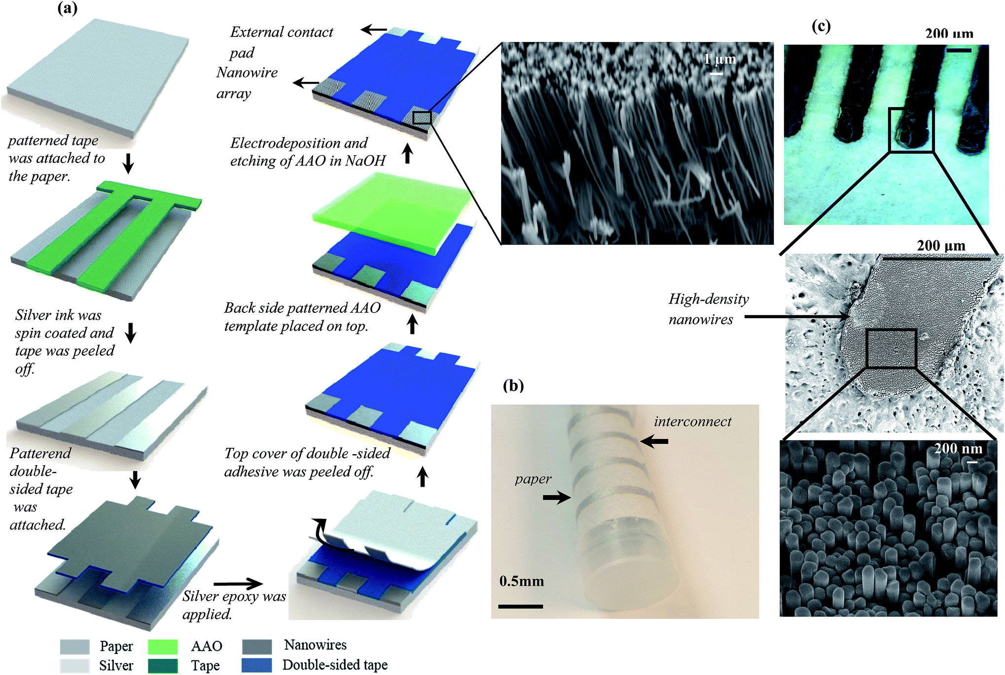 | ||
| Fig. 1 (a) Fabrication process flow of nanowire electrodes on paper. Details of individual steps are mentioned in the figure above. Additional details: for patterning of tape, laser cutter is used. For converting patterned hydrophobic areas to hydrophilic, laser or plasma treatment is utilized before applying silver ink. (b) Shows wrapped paper with nanowires. (c) Patterned electrodes on the paper after the growth of nanowires. | ||
In the next step, patterned interconnects on the paper were covered and a conductive epoxy (Norland NCA130) was screen printed on the patterned paper-based electrodes; cover of the double-sided tape was peeled off, and the AAO template with patterned electrodes was then attached on the paper; the epoxy was cured using UV light and heat (2 hours, 80 °C) to completely cure and provide a good electrical connection. The size of the patterned electrodes on the paper is larger than the size of electrodes on the AAO to provide simple alignment. We should point out that we have used two kinds of adhesive tapes: first a single sided adhesive tape was used as a mask for fabrication of electrodes and interconnects. Second, a double-sided tape was used to specify the zones for nanowire deposition. It was used to cover all areas on substrate except the areas for electrodes and pads. Moreover, the tape also serves as temporary attachment to AAO template. In essence, multiple adhesive tapes served here as mask to define and pattern regions for interconnect, electrode and substrate and for removal of AAO.
In a second method, which is much simpler, after first step, patterning of double-sided tape and its plasma treatment, which is similar to the first approach, a ∼50 μm thick silver inks was spin-coated on the paper (1000 rpm for 60 s). Then the cover of the double-sided tape was removed and the AAO template was attached carefully. After applying a uniform force, the attached side of the AAO template was filled with silver ink, left in the oven (121 °C, one hour), and then placed in the desiccator overnight to completely remove all the remaining solvents. Thickness of the spin-coated silver ink is equal to the thickness of the double-sided tape, so a thinner double-sided tape works better. Distance between electrodes was chosen to be large enough to not disturb each other while force was applied. Based on estimation, distance between the electrodes should be 10 times larger than the electrode diameter. This gap between electrodes is very typical for most applications like electrochemical sensors.46 In this approach, silver ink attached between paper and the AAO template was used as a seed layer electrode for electrodeposition. There is no need for patterning the electrodes on the AAO template. An advantage of the second approach with respect to the first approach is simplicity, robustness, and lower cost. However, its bottleneck is the roughness of the cured silver ink as a seed layer, which may affect the density and consistency of the nanowires.
The electrodeposition was performed using chronopotentiometry method with a current density of 1 mA cm−2 by utilizing Potentiostat (PGSTATN12, Autolab, Mterohm) for several hours depending on the desired length of nanowires. After electrodeposition, the AAO template was etched in sodium hydroxide (20 mL, 2 M) for 1 hour. For electrodeposition and etching, the 3D-printed electrochemical cell has been used. Fig. 1c shows patterned nanowire electrodes on the paper.
One of the concerns in electrodeposition is the quality of the seed layer for electroplating. In the second approach we employed the cured silver ink as the seed layer. The impedance measurement in the dry state shows 1.16 Ω over a wide range of frequency (see Fig. S1†). The wet state demonstrates the high kinetic transport of the silver ink electrode which is comparable with a sputtered silver electrode. The measured impedance varies between 700 Ω to 500 Ω which is due to the ohmic drop of a 0.1 M phosphate buffer electrolyte between the silver-ink electrode and Ag/AgCl as a reference electrode.
Results and discussion
The growth of nanowires with the desired length and diameter is one of the critical design parameters in such high density nanowire electrodes on paper. In general, varying the time of deposition or current density or the thickness of the AAO template or the nature and type of the electrodeposited materials, or the concentration of electrodeposition bath will control the length of nanowires in the proposed template-assisted approach. Current density affects the quality of deposition; it should always be kept as low as possible (less than 5 mA cm−2) to get a uniform electrodeposition. Here we have used a current density of 1 mA cm−2, which gives a deposition rate of 20 nm min−1. The thickness of Whatman AAO templates are 60 μm so the maximum length of nanowire is limited to 60 μm. Electrodeposition time is the most effective parameter in controlling the length of nanowires; a longer time would cause longer nanowires. For example, we have performed copper electrodeposition for 1 hour, 2 hours, and 5 hours, and nanowires that resulted in growth of nanowires of lengths of 2, 5, and 10 μm respectively. Moreover, another parameter that controls length and morphology of nanowires is the type of material itself. Voltage during deposition of the copper is kept very small ∼0.2 V; for nickel it is ∼0.6 V, and for platinum it is high ∼1.5 V. These numbers were obtained empirically and the differences could be because of the different reduction potential of plating materials and resistivity of the plating solutions, with copper solution being the least resistive (Table 1).| Electroplated metal | Voltage (V) |
|---|---|
| Nickel | 0.6 |
| Copper | 0.2 |
| Platinum | 1.5 |
The second parameter in growth of nanowires is its diameter, which is limited to the pore size of the AAO template. In this study, we used a commercial Whatman AAO template with pore size of 20 nm and 200 nm. The SEM images in Fig. 2a and Fig. 2b show nickel nanowire with these two different diameters. However, electrodeposition of high-density nanowires on paper has some other issues which should also be considered. Paper is quite lightweight and is not very stable during electrodeposition, it might move physically over long deposition time. Utilizing double-sided tape and applying uniform force with a clamp inside a custom 3D-printed cell made paper more stable during deposition in our experiments. In this case, double-sided tape should be smooth and the clamp tight enough to not let solution go through the pores of the AAO template into the unpatterned areas. Leaking of the solution into the unpatterned area reduces the electrodeposition rate but will not stop the nanowire growth. It is also better to use solvent resistant tape to increase the stability and lifetime of tape in solution.
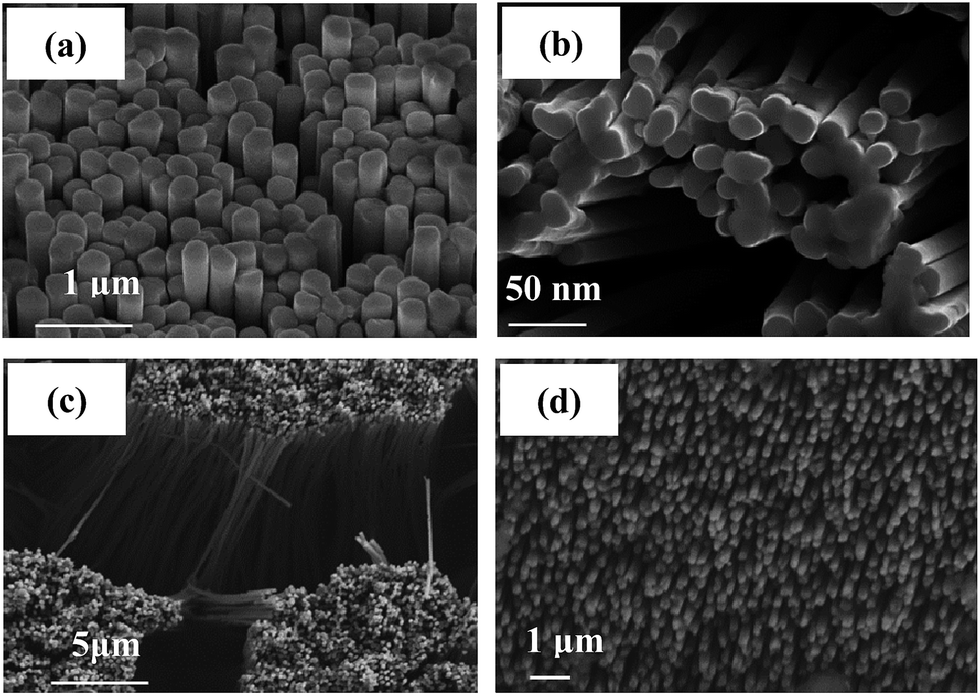 | ||
| Fig. 2 SEM images of high-density nanowires on paper (a) nickel nanowires with diameter of 200 nm (b) nickel nanowires with diameter of 20 nm (c) copper nanowires with diameter of 20 nm (d) platinum nanowires with diameter of 20 nm. | ||
Another issue, which may also be problematic, is the unwanted soaking of the paper from the solution even in areas where there are no electrodes. Using hydrophobic paper like a parchment paper, wax paper, or photography paper could solve this problem. Another solution is to use wax printing to form a hydrophobic channel around the electrodes, which will limit the flow of the solution only in the hydrophillic areas. Details can be found in previous studies.3,47
Electrode characterization
For the physical characterization of nanowires, scanning electron microscopy (SEM) and energy-dispersive X-ray spectroscopy (EDS) have been used. SEM images of nanowire electrodes were acquired using FESEM ultra55 (12 kV) to determine the structural features of the fabricated nanowires on the paper substrate. Samples were mounted on the aluminum stubs using conductive carbon paint. As shown in Fig. 2, we successfully grew nickel nanowires (Fig. 2a and b), copper nanowires (Fig. 2c) and platinum nanowires (Fig. 2d). Fig. 2a and b show nickel nanowires with diameters of 200 nm and 20 nm. Copper nanowires with length of more than 10 μm are achieved (Fig. 2c). We used EDS for investigation of the nanowires composition. The electron beam from SEM tools excited the sample and an X-ray spectrum emitted by the sample was obtained using the X-ray detector. Results of EDS analysis for nickel, copper and platinum high-density nanowires are shown in Fig. 3. | ||
| Fig. 3 EDS analysis of different types of nanowire on paper (a) copper nanowire, (b) platinum nanowire, and (c) nickel nanowire. | ||
The high surface area of nanowires, which is another unique aspect of high-density nanowires, is confirmed by measuring impedance of the electrode–electrolyte interface.
A high-density nanowire electrode with a diameter of 2.4 cm and Ag/AgCl served as an anode and cathode respectively. A phosphate buffer solution with pH of 7.4 was used as an electrolyte and a LCR Meter (Agilent E4980A) was utilized for the measurement of the impedance spectra (Fig. 4e). An impedance model of the electrode–electrolyte interface is shown in Fig. 4f. Based on the model, charge transfer resistance and double layer capacitance are the dominant variable parameters at the low and intermediate frequency range respectively. Solution resistance and interconnect resistance, which are the two constants play a significant role only at very high frequency.
 | ||
| Fig. 4 Impedance measurement of copper bare electrode and copper nanowire electrodes both on paper. (a) Bode plot – magnitude. (b) Bode plot – phase. (c) Nyquist plot of nanowire electrode. (d) Nyquist plot of bare electrode. (e) Impedance measurement test set up. (f) Impedance model where RC, RCT, CD, and RS are interconnect resistance, charge transfer resistance, double layer capacitance and electrolyte solution resistance respectively. | ||
Since charge transfer is negligible in the buffer electrolyte, effect of its resistance is not significant. Moreover, the buffer electrolyte is chosen to be highly conductive. Therefore the most useful frequency range for surface area information is the intermediate frequency (500 Hz to 2 MHz). The Bode plot shows that the impedance magnitude reduces when a nanowire electrode is used (see Fig. 4a). The X-axis intercept in the Nyquist plot shows ∼1000 Ω for both electrodes which refers to the resistance of the solution and the interconnect combined. When frequency goes higher than 2 MHz, the impedance in the nanowire-based electrode becomes less than that of the bare electrode because of the higher double layer capacitance (CD) resulting from its higher surface area. Impedance model analysis shows significant enhancement of the surface area in nanowire-based electrode.
From an application point of view, the platinum nanowire is a strong electrocatalyst metal and is used for numerous electrochemical sensors.45,48 Since biodegradable cellulose papers have recently been discovered, growth of nanowire on the paper using biocompatible materials provides the opportunity of using these high quality electrodes in implantable devices.
Moreover, platinum is an inert metal and it can be used for long term monitoring, utilizing the high conductivity and electrical transport of nanowires along with wearability of the paper, making it an appropriate electrode for ECG. This will be discussed in Electrocardiography section.
Energy harvesting
Harvesting energy from natural acidic environments such as body fluids such as sweat, urine, gastric juice forms the basis of the proposed battery. Recently, we proposed energy harvesting from gastric juice in the digestive tract.49 This battery is essentially a galvanic cell in which an electroactive metal like zinc oxidizes and generates electrons. The generated electrons are used for reduction of hydrogen ions coming from the acidic environment.In this study, we replace the traditional cathode electrode with a high-density nanowire electrode. Zinc and platinum nanowire electrode served as an anode and cathode respectively. For fabrication, two silver electrodes were patterned on paper using a screen-printing approach. Then zinc was electroplated on one electrode as the anode, and then a nanowire electrode was fabricated using the previously mentioned approach. Nafion (5 mL) was dropped on the cathode and left to dry overnight at room temperature. We have characterized device using a simulated gastric acidic solution with background contaminants, made using SIF powder (Biorelevent, Surrey, UK), and NaCl (400 mg) in DI water (200 mL), and pH was adjusted to 1.6 using hydrochloric acid (which models the gastric environment pH ranges from 1 to 3). Filter paper was soaked in gastric juice and attached to the paper on which electrodes were fabricated. The open load voltage is 0.84 V (see Fig. 5b). Maximum power of 6.3 mW with 32 mA current was achieved for a 6 Ω load impedance (see Fig. 5c and d), and this reveals that the internal resistance of the battery (∼6 Ω) is improved considerably with respect to the previous work.49 One can envision utilizing this battery as part of an ingestible pill for smart drug dosage.
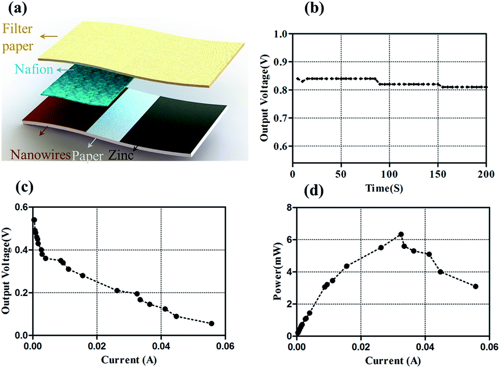 | ||
| Fig. 5 Energy harvesting results using nanowire electrode on paper as a cathode, and simulated gastric juice as an electrolyte (a) structure of the battery. (b) Transient response (c) output voltage (d) output power. | ||
Electrocardiography
Cardiovascular diseases are the leading cause of the death in the world.50 One could manage chronic heart conditions by continuous monitoring of electrocardiogram (ECG) activity. Development of an electrode and device for long term ECG monitoring is therefore essential to monitor heart activity in at-risk patients.The electrodes that interface with the skin are a very important part of such a device to monitor the heart's electrical activity. However, current ECG electrodes typically used for these applications are made from Ag/AgCl with a gel electrolyte interface. It has a tendency to dry up over time and also degrades considerably due to sweat and motion; this consequently affects the quality of the signal received from the heart.51 Moreover wet electrodes are uncomfortable for the patients since direct skin contact is necessary at all times. Recently, dry ECG electrodes have been reported as a promising approach for replacement of wet ECG electrodes because they can facilitate long term monitoring with little inconvenience to the patient.51–54 However, dry electrodes are very sensitive to motion artifacts and poor contact with skin and limited biocompatibility restrict their utility. In this study we have proposed wearable and flexible paper-based nanowire electrode as a viable dry ECG electrode for long term ECG monitoring. Circular ECG electrodes with a diameter of 10 mm were fabricated according to the aforementioned fabrication process. Conceptual demonstration of a high-density nanowire electrode on skin as a dry ECG patch is shown in Fig. 6a. For the evaluation of the ECG electrode, we have used a 3-electrode setup: two nanowire electrodes on paper were connected to the left and right arm, and one regular screen printed silver electrode was connected to left leg as it is shown in Fig. S2b.†
 | ||
| Fig. 6 ECG analysis using nanowire electrode on paper. (a) Conceptual demonstration of high density nanowire electrode on skin as a dry ECG patch. (b) Electrode-skin contact impedance measurement. (c) The recorded ECG signal from a healthy volunteer. | ||
Since the electrical signal is very small and noisy, amplification and filtering is required. In general, one of the main reasons of noise in ECG measurement especially with dry electrode is electrode-contact variation due to motion and respiration. There are different approaches to solve this problem such as using high pass filter with cut off frequency of ∼1 Hz which is effective for motion cancelation. However, design of these elements was not the focus of this research article and can be found elsewhere.1,55
The electrical circuit composed of mentioned components is implemented on a printed circuit board (PCB) using the circuit topology previously discussed.56 Details are explained in Fig. S2c.†
Flexibility and easy attachment of the nanowire on paper electrode using a double-sided tape on the human body will make for a very easy method to interface the electrode system for obtaining these measurements. As mentioned earlier, a critical aspect to receive a high fidelity ECG signal is a good contact between electrodes and skin. The electrode-skin contact impedance has been measured to characterize the proposed ECG electrode. For the measurement of the impedance interface, the configuration which is shown in Fig. 6b(i) was used based on an approach proposed in previous studies.57 In this set up, 3 electrodes (A, B, and C) were attached to the skin. Electrode B is the main electrode, which is addressable for the measuring of its contact impedance with skin. Current in the range of 1–20 μA (using a function generator and Rext) is applied to electrode A while B and C are in open load. The voltage measured between electrodes B and C (Vout) is only function of voltage drop across the tissue-electrode impedance for electrode B (Re2 = Vout/Iin). As Fig. 6b(ii) shows, impedance magnitude changed from 100 kΩ to 1 kΩ when frequency varied from 5 Hz to 1.5 kHz.
The recorded ECG signal using these electrodes is shown in Fig. 6c. Q, R, S and T waves which reflect the rapid depolarization of the right and left ventricles are labelled on the graph. The results are very similar to those from commercially available ECG electrodes. Moreover, since the paper is foldable and flexible, and nanowires establish better contact in motion, the proposed ECG electrode provides more stable measurements even in a dry state without the need for any wet-gel adhesives.
Conclusions
In conclusion, we presented a simple room-temperature approach to grow and pattern high-density nanowire electrodes on paper substrates. This is a first time that electrodeposition of nanowires patterning has been performed on paper substrates. The approach we presented is significant for its low cost through primary use of cheap raw materials (paper, adhesive tapes) in a room-temperature process. The approach also enables different nanowire electrodes on the same paper substrate. This has enabled one to bring the advantage of nanotechnology to paper based diagnostics.For proof of concept, different types of metal nanowires with different lengths were grown on paper substrates and successfully characterized using SEM and EDS measurements. The approach utilized electrodeposition of nanowires through nanoporous template on conductive electrodes that were printed and patterned on paper. Initial electrode pattern which serves as a seed layer for electrodeposition is made either from a eutectic alloy of gallium–indium or sputtered silver or conductive silver ink. It uses dle-sided adhesive tape for patterning and release in a benchtop room-temperature approach. The nanowires on paper electrodes provide very high surface area and low electrode impedance making it suitable for a wide range of applications. We showed that this electrode could be a viable dry alternative to wet gel electrodes for recording of the electrocardiogram (ECG) signal. Impedance between skin and an electrode was measured and it varied from 100 kΩ to 1 kΩ when frequency was swept from 5 Hz to 1.5 kHz, and was found to be comparable to the values found in the literature for a good quality electrode. In another application, we utilized nanowire electrode on paper as a cathode in an acidic battery and it provided a significant amount of power around 6 mW which can be employed for powering an endoscopy capsule. Beyond these applications, the proposed approach for fabrication of nanowire electrodes on paper opens other opportunities that bring the promise of nanomaterials and nanotechnology to paper-based devices while also keeping the advantages of low-cost and ease of fabrication for paper-based platforms. Such examples include realization of chemical and biological sensors, electrodes for supercapacitors and batteries and environmental applications.
Acknowledgements
The Device was fabricated at the Tufts Micro and Nanofabrication Facility (TMNF). Project was funded by the National Science Foundation ECCS-0955024 and EFRI-1240443. SEM images were acquired at Harvard University Center for Nanoscale System (CNS). We also would like to acknowledge Meera Punjiya, Sara Mostafalu and Samuel Macnaughton for their help with experiments.Notes and references
- Z. Zhang, I. Silva, D. Wu, J. Zheng, H. Wu and W. Wang, Med. Biol. Eng. Comput., 2014, 52, 1019–1030 Search PubMed.
- A. W. Martinez, S. T. Phillips, G. M. Whitesides and E. Carrilho, Anal. Chem., 2009, 82, 3–10 CrossRef PubMed.
- Z. Nie, C. A. Nijhuis, J. Gong, X. Chen, A. Kumachev, A. W. Martinez, M. Narovlyansky and G. M. Whitesides, Lab Chip, 2010, 10, 477–483 RSC.
- J. R. Windmiller and J. Wang, Electroanalysis, 2013, 25, 29–46 CrossRef CAS.
- J. Shah and R. Malcolm Brown Jr, Appl. Microbiol. Biotechnol., 2005, 66, 352–355 CrossRef CAS PubMed.
- A. H. Najafabadi, A. Tamayol, N. Annabi, M. Ochoa, P. Mostafalu, M. Akbari, M. Nikkhah, R. Rahimi, M. R. Dokmeci, S. Sonkusale, B. Ziaie and A. Khademhosseini, Adv. Mater., 2014, 26, 5823–5830 CrossRef CAS PubMed.
- E. J. Maxwell, A. D. Mazzeo and G. M. Whitesides, MRS Bull., 2013, 38, 309–314 CrossRef CAS.
- A. D. Mazzeo, W. B. Kalb, L. Chan, M. G. Killian, J.-F. Bloch, B. A. Mazzeo and G. M. Whitesides, Adv. Mater., 2012, 24, 2850–2856 CrossRef CAS PubMed.
- M. Punjiya, P. Mostafalu and S. Sonkusale, Low-cost paper-based electrochemical sensors with CMOS readout IC, BioCAS, IEEE, 2014, 324–327 Search PubMed.
- G. Chitnis, Z. Ding, C.-L. Chang, C. A. Savran and B. Ziaie, Lab Chip, 2011, 11, 1161–1165 RSC.
- Y. Chen, Y. Zilberman, P. Mostafalu and S. R. Sonkusale, Biosens. Bioelectron., 2014 DOI:10.1016/j.bios.2014.09.010 ISSN 0956-5663.
- Y. Lu, W. Shi, L. Jiang, J. Qin and B. Lin, Electrophoresis, 2009, 30, 1497–1500 CrossRef CAS PubMed.
- A. W. Martinez, S. T. Phillips, M. J. Butte and G. M. Whitesides, Angew. Chem., Int. Ed., 2007, 46, 1318–1320 CrossRef CAS PubMed.
- A. W. Martinez, S. T. Phillips, B. J. Wiley, M. Gupta and G. M. Whitesides, Lab Chip, 2008, 8, 2146–2150 RSC.
- R. H. Müller and D. L. Clegg, Anal. Chem., 1949, 21, 1123–1125 CrossRef.
- K. Abe, K. Suzuki and D. Citterio, Anal. Chem., 2008, 80, 6928–6934 CrossRef CAS PubMed.
- X. Li, J. Tian, T. Nguyen and W. Shen, Anal. Chem., 2008, 80, 9131–9134 CrossRef CAS PubMed.
- A. C. Siegel, S. T. Phillips, M. D. Dickey, N. Lu, Z. Suo and G. M. Whitesides, Adv. Funct. Mater., 2010, 20, 28–35 CrossRef CAS.
- R. MacKenzie, C. Fraschina, B. Dielacher, T. Sannomiya, A. B. Dahlin and J. Voros, Nanoscale, 2013, 5, 4966–4975 RSC.
- A. Vlad, A. L. M. Reddy, A. Ajayan, N. Singh, J.-F. Gohy, S. Melinte and P. M. Ajayan, Proc. Natl. Acad. Sci. U. S. A., 2012, 109, 15168–15173 CrossRef CAS PubMed.
- H. Y. Jung, M. B. Karimi, M. G. Hahm, P. M. Ajayan and Y. J. Jung, Sci. Rep., 2012, 2, 1–5 Search PubMed.
- P. Mostafalu and S. Sonkusale, Paper-based super-capacitor using micro and nano particle deposition for paper-based diagnostics, IEEE Sensors, 2013, 1–4 Search PubMed.
- G. Ren, D. Hu, E. W. C. Cheng, M. A. Vargas-Reus, P. Reip and R. P. Allaker, Int. J. Antimicrob. Agents, 2009, 33, 587–590 CrossRef CAS PubMed.
- U. Samuel and J. P. Guggenbichler, Int. J. Antimicrob. Agents, 2004, 23(suppl. 1), 75–78 CrossRef PubMed.
- J. Chen, F. Saeki, B. J. Wiley, H. Cang, M. J. Cobb, Z.-Y. Li, L. Au, H. Zhang, M. B. Kimmey, X. Li and Y. Xia, Nano Lett., 2005, 5, 473–477 CrossRef CAS PubMed.
- Z.-Z. J. Lim, J.-E. J. Li, C.-T. Ng, L.-Y. L. Yung and B.-H. Bay, Acta Pharmacol. Sin., 2011, 32, 983–990 CrossRef CAS PubMed.
- H. Shen, J. You, G. Zhang, A. Ziemys, Q. Li, L. Bai, X. Deng, D. R. Erm, X. Liu, C. Li and M. Ferrari, Adv. Healthcare Mater., 2012, 1, 84–89 CrossRef CAS PubMed.
- M. Heim, B. Yvert and A. Kuhn, J. Physiol., 2012, 106, 137–145 CrossRef PubMed.
- E. Seker, Y. Berdichevsky, M. R. Begley, M. L. Reed, K. J. Staley and M. L. Yarmush, Nanotechnology, 2010, 21, 125504 CrossRef PubMed.
- R. Esfandyarpour, H. Esfandyarpour, J. S. Harris and R. W. Davis, Nanotechnology, 2013, 24, 465301 CrossRef PubMed.
- R. Esfandyarpour, H. Esfandyarpour, M. Javanmard, J. S. Harris and R. W. Davis, Sens. Actuators, B, 2013, 177, 848–855 CrossRef CAS PubMed.
- P. Tyagi, D. Postetter, D. L. Saragnese, C. L. Randall, M. A. Mirski and D. H. Gracias, Anal. Chem., 2009, 81, 9979–9984 CrossRef CAS PubMed.
- Y. Wang, Y. Zhu, J. Chen and Y. Zeng, Nanoscale, 2012, 4, 6025–6031 RSC.
- P. Xie, Q. Xiong, Y. Fang, Q. Qing and C. M. Lieber, Nat. Nanotechnol., 2012, 7, 119–125 CrossRef CAS PubMed.
- D. E. Perea, E. R. Hemesath, E. J. Schwalbach, J. L. Lensch-Falk, P. W. Voorhees and L. J. Lauhon, Nat. Nanotechnol., 2009, 4, 5 CrossRef PubMed.
- Y. Wu and P. Yang, J. Am. Chem. Soc., 2001, 123, 3165–3166 CrossRef CAS.
- D. Wang and H. Dai, Angew. Chem., 2002, 114, 4977–4980 CrossRef.
- J. C. Hulteen and C. R. Martin, J. Mater. Chem., 1997, 7, 1075–1087 RSC.
- R. B. Sadeghian and M. Kahrizi, Sens. Actuators, A, 2007, 137, 248–255 CrossRef CAS PubMed.
- R. Banan-Sadeghian, S. Badilescu, Y. Djaoued, S. Balaji, T. Vo-Van and M. Kahrizi, IEEE Electron Device Lett., 2008, 29, 312–314 CrossRef CAS.
- A. K. Bentley, M. Farhoud, A. B. Ellis, A.-M. L. Nickel, G. C. Lisensky and W. C. Crone, J. Chem. Educ., 2005, 82, 765 CrossRef CAS.
- J. Byun, J. I. Lee, S. Kwon, G. Jeon and J. K. Kim, Adv. Mater., 2010, 22, 2028–2032 CrossRef CAS PubMed.
- J.-H. Cho and S. T. Picraux, Nano Lett., 2013, 13, 5740–5747 CrossRef CAS PubMed.
- J. Hu, S. Wang, L. Wang, F. Li, B. Pingguan-Murphy, T. J. Lu and F. Xu, Biosens. Bioelectron., 2014, 54, 585–597 CrossRef CAS PubMed.
- M. Yang, F. Qu, Y. Lu, Y. He, G. Shen and R. Yu, Biomaterials, 2006, 27, 5944–5950 CrossRef CAS PubMed.
- H. Sungkil, C. N. LaFratta, V. Agarwal, Y. Xin, D. R. Walt and S. Sonkusale, IEEE Sens. J., 2009, 9, 609–615 CrossRef.
- A. K. Yetisen, M. S. Akram and C. R. Lowe, Lab Chip, 2013, 13, 2210–2251 RSC.
- I. Dumitrescu and R. M. Crooks, Proc. Natl. Acad. Sci. U. S. A., 2012, 109, 11493–11497 CrossRef CAS PubMed.
- P. Mostafalu and S. Sonkusale, Biosens. Bioelectron., 2014, 54, 292–296 CrossRef CAS PubMed.
- World Health Organization, Global status report on noncommunicable diseases 2010, Geneva, 2011 Search PubMed.
- J. Ha-Chul, M. Jin-Hee, B. Dong-Hyun, L. Jae-Hee, C. Yoon-Young, H. Joung-Sook and L. Sang-Hoon, IEEE Trans. Biomed. Eng., 2012, 59, 1472–1479 CrossRef PubMed.
- G. S. Jeong, D.-H. Baek, H. C. Jung, J. H. Song, J. H. Moon, S. W. Hong, I. Y. Kim and S.-H. Lee, Nat. Commun., 2012, 3, 977 CrossRef PubMed.
- J.-W. Jeong, M. K. Kim, H. Cheng, W.-H. Yeo, X. Huang, Y. Liu, Y. Zhang, Y. Huang and J. A. Rogers, Adv. Healthcare Mater., 2014, 3, 642–648 CrossRef CAS PubMed.
- N. Meziane, J. G. Webster, M. Attari and A. J. Nimunkar, Physiol. Meas., 2013, 34, R47 CrossRef CAS.
- M. L. Ahlstrom and W. J. Tompkins, IEEE Trans. Biomed. Eng., 1985, BME-32, 708–713 CrossRef PubMed.
- Texas Instruments, INA118 datasheet, 1998.
- M. S. Spach, R. C. Barr, J. W. Havstad and E. C. Long, Circulation, 1966, 34, 649–656 CrossRef CAS.
Footnote |
| † Electronic supplementary information (ESI) available: Impedance measurement of silver ink, electrodeposition cell, ECG configuration set up, schematic of read out electronic, and recorded ECG signal. See DOI: 10.1039/c4ra12373e |
| This journal is © The Royal Society of Chemistry 2015 |