Molecular dynamics simulation of deformation accumulation in repeated nanometric cutting on single-crystal copper

Lin Zhangab, Hongwei Zhao*b, Lu Daic, Yihan Yangb, Xiancheng Dub, Pengyi Tanga and Li Zhanga
aDepartment of Mechanical and Automation Engineering, The Chinese University of Hong Kong, Shatin, Hong Kong SAR, China
bSchool of Mechanical Science and Engineering, Jilin University, Changchun 130025, China. E-mail: hwzhao@jlu.edu.cn
cSchool of Mathematics and Physics, Suzhou University of Science and Technology, Suzhou 215009, China

Received 14th October 2014 , Accepted 22nd December 2014

First published on 23rd December 2014


Abstract

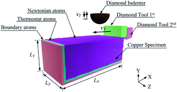
The machining-induced residual defects and stress in subsurfaces determine the mechanical properties of the finished surfaces of bulk materials. In this paper, three-dimensional molecular dynamics simulations of AFM-based nanoindentation using diamond indenters are conducted on machining-induced surfaces of single-crystal copper. The simulation results indicate that the residual defects and deformation introduced from the first nanometric cutting process induce dislocation nucleation and propagation in the successive nanometric cutting process. A large number of atomic defects and vacancies occur in the second nanometric cutting process, many more than in the first cutting process, leading to a significant change in mechanical properties. In addition, the quantitative analysis of the surface is obtained based on the Oliver–Pharr method. The results reveal that the machining-induced surface is softer than the pristine single-crystal copper surface. Based on the defect accumulation limitation, the hardness and surface potential energy of the machining-induced surface tend to be between the highest and lowest limitations.


Introduction

Ultra-precision nanometric machining with diamond tools, which can remove materials at the nanoscale, has been widely employed to produce nanometric finished surfaces with sub-micron-level accuracy for components.1 Since there is an increasing demand for the manufacture of miniaturised components in the fields of aerospace,2 medical instruments,3 communication systems,4 micro-/nano-electromechanical systems (MEMS/NEMS)5 and micro-/nanorobotics,6,7 the single-point diamond turning (SPDT) technique has attracted the attention of researchers worldwide. In order to manufacture well-made components, the material removal mechanisms and mechanics at the atomic scale, including chip formation, must be fully investigated, including factors such as machining-induced surface properties and elastic and plastic deformation.

Mechanical manufacturing may cause changes in the structures and other physical properties of machining-induced surfaces or substrates. The hardness and friction coefficient of a machined surface are related to the pressure exerted on the material, especially at the micro-/nano-scale; not only is the size itself reduced substantially, but the physical and chemical characteristics of the material also change.8 In spite of the rapid development of fabrication techniques, the fundamental understanding of atomic structural changes taking place beneath the surface in the nanometric cutting process is still far from complete. As nanometric cutting involves changes in only several layers of atoms adjacent to the surface, there are many experimental difficulties in the in situ observation of defect occurrences and dislocation motions inside materials of such dimensions. On the other hand, large-scale computer simulations with atomic resolution can, with relative ease, provide us with details of the mechanism of deformation induced by nanometric cutting.9

The material removal mechanism and deformed layer of nanometric cuttings have been widely investigated with the aid of molecular dynamics (MD) simulation. For instance, Maekawa et al. studied the friction between single-crystal copper and a diamond-like tool at the nanometric scale orthogonal machining.10 Zhang and Tanaka studied the wear and friction at the atomic scale and identified four distinct regimes of deformation in nanometric machining, the no-wear, adherence, ploughing, and cutting regimes.11 Komanduri and co-workers investigated the effects of crystal orientation, cutting direction and tool geometry on the nature of deformation and machining anisotropy of the material with the aid of MD simulation.12 More recently, Zhang et al. conducted MD simulations of nanometric cuttings on single-crystal copper and established a criterion based on single-atom potential energy variation.13

The previous studies mentioned above,10,11,13 however, introduced the material removal mechanism of the nanometric cuttings on pristine single-crystal copper specimens. In fact, since the final finish surface usually involves multiple processing procedures, the study of successive processing on the machining-induced surface with initial defects and residual stress could be even more critical. Thus, the results obtained from a single nanometric cutting process are not sufficient to provide a complete understanding of the mechanism of deformation in the successive processes. Moreover, the deformation criterion in nanometric cutting process based on atomic potential energy13 is not easily obtained using current experimental equipment.

Nanoindentation is one of the most frequently used techniques to measure the mechanical properties of a surface, such as Young's modulus and hardness.14 Hardness indicates a resistance to penetration or permanent deformation. There are various definitions of hardness from field to field. The most commonly used definition for nanoindentation testing is Meyer hardness, which corresponds to the mean contact pressure at full load.15 In a nanoindentation test, the size of the residual impression is often only a few microns, making it very difficult to obtain a direct measurement using optical techniques. Instead, the depth of penetration beneath the specimen surface is measured as the load is applied to the indenter. To date, numerous studies have employed nanoindentation to investigate the mechanical properties and characteristics of materials. Some researchers reported the observation of machining-induced phase transformations after nanometric cutting experiments. Yan et al. measured the mechanical properties and characteristics of single-point diamond turning silicon specimens via nanoindentation tests16,17 and found that the machining-induced amorphous layers combine high micro-plasticity and low hardness. Zhang et al. conducted a nanometric simulation of repeated single-point diamond turnings of monocrystalline silicon20 and discovered that the amorphous phase silicon deforms and behaves differently in the second nanometric cutting process. Larger resistance induces an increase in the local temperature between the cutting tool and the amorphous layer during the second process. They also performed nanoindentation followed by nanometric cutting along different crystal orientations and compared the machining-induced new surface with pristine single-crystal copper.21 Although the different types of dislocation nucleation and hardness of the two kinds of surfaces were analysed, the defects and deformation accumulation were not taken into account.

In this paper, we report how single-crystal copper will behave under repeated nanometric cutting processes. A series of three-dimensional MD simulations are conducted on a single-crystal copper specimen with repeated cuttings by diamond tools. Nanoindentations are conducted to quantitatively study the surface mechanical properties (Young's modulus and hardness). Moreover, the damage accumulation and the softening effect on the processed surface are characterised. The subsequent parts of this paper are arranged as follows: in Section II, the construction of the MD simulation models and the selection of model parameters as well as the selection of cutting parameters are described; in Section III, the mechanism of the second cutting process is revealed by identifying the movement of dislocations; in Section IV, the calculation of mechanical properties based on nanoindentation curves and the explanation of the deformation accumulation are presented; and finally, the major findings are summarised in the last section.

Simulation methodology

Initial model

Fig. 1 schematically shows the physical model of a single-crystal copper specimen, two diamond tools and a hemispherical diamond indenter used in the simulation. The diamond hemispherical indenter contains 16[thin space (1/6-em)]960 carbon atoms with a radius of 50.0 Å. The two diamond tools have the same geometrical parameters and shapes. The rake angle and clearance angle are 0° and 7°, respectively, and the tool edge is 1.0 nm. Since the hardness of copper is much less than that of diamond, the tools and indenter are assumed to create no deformation or wear in the simulation. In order to eliminate the boundary effects, the dimension of the specimen should be many times larger than that of the interaction zone; however, this could challenge the current computational capability. Taking this contradiction into consideration, the optimum volume of the specimen should not influence the displacement and velocities of the atoms during the nanometric cutting and nanoindentation processes.18 The optimum substrate volume obtained from simulations is 37.947 nm × 14.456 nm × 18.070 nm.18 The boundary conditions of the MD simulations involve five layers of atoms in the YZ planes (the left side of the specimen) and the XZ planes (the bottom of the specimen), which are fixed to reduce the boundary effect in the simulation. The velocity and acceleration of other atoms in the specimen remain strictly within the limits of Newton's laws of motion. In order to control the temperature of the specimen during the simulation, the five layers close to the boundary layer are used to absorb the heat from the primary cells.
image file: c4ra12317d-f1.tif
Fig. 1 Molecular dynamics (MD) simulation model of a single-crystal copper specimen, diamond indenter and diamond tools. The control volume of the specimen is LX × LY × LZ = 37.947 nm × 14.456 nm × 18.070 nm.

Potential energy function

The selection of potential energy functions affects the accuracy of the simulation results, which determines the credibility and reliability of the simulation results accordingly.20 In the simulation, the embedded atom method (EAM) potential, which is applied in modelling the mechanical properties of bulk metal materials, is used to dictate the interactions between copper atoms.18 The basic form of the EAM (total energy for an atomic system Etot), which evolved from density function theory, is the totality of the pair-wise potential of the nearest neighbour atoms (ϕ) and the embedding energy (F), which is related to the ‘electron sea’ in which the atoms are embedded. Even with an additional density-dependent term, the pair potentials cannot provide an adequate description of metallic systems. An alternative, simple, but rather realistic approach to the description of bonding in metallic systems is based on the concept of local density, which is considered an important variable. This allows one to account for the dependence of the strength of individual bonds on the local environment, which is especially important for the simulation of surfaces and defects. The total potential energy of the system is expressed by,
 
image file: c4ra12317d-t1.tif(1)
where Etot is the total potential energy of the system, ϕij is the pair potential between atoms i and j, rij is the distance between the atoms i and j, Fi(ρi) is the embedded energy of atom i, ρi is the host electron density at atom i induced by all the other atoms in the system, and ρi is given by,
 
image file: c4ra12317d-t2.tif(2)
where ρi(rij) is the contribution to the electronic density at the site of the atom i, and rij is the distance between the atoms i and j.

The interaction between copper atoms and diamond atoms is modelled by the Morse potential, which can be calculated by,19

 
V(rij) = D(e−2α(rijr0) − 2eα(rijr0)) (3)
where V(r) is the cohesion energy, D is the dissociation energy from the bottom of the potential energy well, α is the elastic modulus, and rij and r0 are the instantaneous and equilibrium distances between two atoms, respectively.

Since the diamond tools and diamond indenter are regarded as rigid bodies in the simulation, the atoms in the diamond tool and indenter are fixed to their initial lattice positions. Therefore, there is no need to employ any potential functions to describe the interactions between C–C atoms. The C–C interactions between the atoms in the diamond tools and diamond indenter are ignored.

Simulation approach

In order to simulate the fabrication and measurement under room-temperature conditions, the single-crystal copper atoms are set in a face-centred cubic (FCC) structure at an ambient temperature of 296 K under the microcanonical (NVE) ensemble. The velocity distribution of the atoms in the specimen is generated from the Maxwell–Boltzmann distribution. In the nanometric cutting simulation, when the temperature of the thermostat atoms varies more than 10 K from the pre-set temperature (296 K), the velocities of the thermostat atoms are rescaled, and the temperature returns to the normal ambient temperature. This method allows heat diffusion from the machining region to the surroundings in much the same way as in the experiments.

Fig. 2 shows the procedures for the repeated nanometric cutting processes, relaxation and nanoindentation on the machining-induced surface. The first diamond tool cuts the surface along the [[1 with combining macron]00] on the XZ plane (marked with 1). After a period of relaxation, the system settles back to another state of equilibrium. The second tool begins to move along the machined surface with the same cutting direction as the first one (marked with 2). After the second nanometric cutting process and relaxation, the diamond indenter moves along the [0[1 with combining macron]0] direction and finally returns to its initial position (marked with 3).


image file: c4ra12317d-f2.tif
Fig. 2 The schematic diagrams of the simulation, (a) procedures of molecular dynamics simulation and (b) the timetable of the simulation.

The large-scale three-dimensional MD simulations are performed by the Large-scale Atomic/Molecular Massively Parallel simulator (LAMMPS) developed by Plimpton.22,23 Parallel computing is realised with the help of the message passing interface (MPI) library. Due to the large computational load, eight computation servers are connected with an Ubuntu Linux operation system, for a total of 256 cores and 128 G of memory. More computational parameters used in the current simulations are shown in Table 1.

Table 1 Computational parameters used in the MD simulation model
Materials Substrate: copper Tool: diamond (rigid) Indenter: diamond (rigid)
Potential function EAM None None
Dimensions 105a × 40a × 50a (lattice constant a = 0.3614 nm) Rake angle: 0° clearance angle: 7° Hemisphere indenter radius: 50.0 Å
Time step 1 fs 1 fs 1 fs
Original temperature 296 K    
Number of atoms 831[thin space (1/6-em)]600 25[thin space (1/6-em)]520 16[thin space (1/6-em)]960
Cutting depth 1.0 nm/time    
Cutting velocity [[1 with combining macron]00] on (010) surface 200 m s−1  
Indentation depth     1.0 nm


Results and discussion

In the simulation, the nanometric cutting speed and the indentation speed are set at 200 m s−1 and 50 m s−1, respectively. The entire simulation lasts for 0.5 ns. Since the rates of the nanometric cutting speed, loading and unloading in the MD simulations are much higher than those of real experiments, a qualitative prediction of the structural transformation could be obtained.13

General description of the second cutting process

Before measuring the machining-induced surface mechanical properties, a general description of dislocations and defects beneath the surface is presented. Fig. 3 shows the dislocations and defects distributed on and under the machining-involved surfaces at a cutting distance of 20.0 nm with different perspectives for two successive nanometric cutting processes. The different colours of the atoms in Fig. 3 present various atomic coordination numbers of atoms. Since the copper atoms in the perfect FCC single-crystal, with coordinate number of 12, have been deliberately eliminated, the rest of the atoms and structures in Fig. 3 only involve boundary atoms and defect-related structures inside the specimen of the order of atoms.
image file: c4ra12317d-f3.tif
Fig. 3 Dislocations and defects distributed in the specimen at a cutting distance of 20.0 nm in (A) the first nanometric cutting process and (B) the second nanometric cutting process shown from four views: (I) the interior defects inside the specimen; (II) side view of the specimen; (III) the front view; and (IV) the rear view of the machining surface.

Several types of defects involved in both nanometric cutting processes are marked with numbers in Fig. 3. Most of the vacancies are located under the tool, marked with 1. These vacancies are immobile and remain in the specimen after they are generated from the interactions of dislocations moving in the specimen. The vacancy cluster is independent of the vacancy in the aggregate state, marked 2 in the specimen. Compared with under the first machining-induced surface in Fig. 3(B-I), more vacancies and vacancy clusters gather under the second machining-induced surface, which may influence the mechanical properties of the machining-induced surface.

There are other differences in the distribution of dislocation loops in the specimen, which are regarded as symbols of plastic deformation during the nanometric cutting process. In Fig. 3(B-I), two partial dislocation loops bounding the stacking-fault region, marked with 3, are expelled from the surrounding areas and glide through the thickness of the specimen towards the bottom surface. The dislocations marked with 5 shown in Fig. 3(A-I) are basically the same dislocation type as those marked with 3 and 4, which are expelled in front of the tool and move along the top surface. In Fig. 3(B-II), the dislocations generated in the second cutting process generally form beneath the tool. In the second cutting process, most of the dislocation loops are limited to the nearby region of the tool, affected by residual stress and defects in the specimen.

Fig. 3(A-II) and (B-II) are the side views of the machined surfaces. Compared with the volume of chips in front of the tool, there are more atoms piled up in front of the tool in the first nanometric cutting process. In addition, the trails generated by dislocations, which are highly mobile and interact between themselves and other defects in the specimen, can be clearly seen in front of the chips in the first cutting process. Fig. 3(B-II) clearly shows the distribution of the dislocations in the specimen.

Residual defects and deformation in nanoindentation

The residual defects and stress in the subsurface have a great influence on the mechanical properties of the finished surface, such as hardness and Young's modulus. This is due to the initial defects in the subsurface usually becoming a new source of dislocations and dislocation loops. Therefore, it is necessary to identify the distribution and density of residual defects in the subsurface.

Fig. 4 shows the defects on and inside the specimen before and after successive nanometric cutting processes from two different views. The regions on the surfaces measured in the simulations are surrounded with black lines. Before the nanometric cutting process (Fig. 4(A-I)), there are no defects on the XZ surface or in the specimen since all the atoms of the specimen fluctuate in their original lattice positions. After the first cutting process, some residual defects generated on the machining-induced surface during the first cutting process remain on the surface and in the subsurface. Inside the specimen under the machining-involved surface, an obvious vacancy cluster remains, as shown in Fig. 4(B-II).


image file: c4ra12317d-f4.tif
Fig. 4 Residual dislocations and defects in the machined surface and inside the specimen (A) before the first cutting process, (B) before the second cutting process, and (C) after the second cutting process from two different views: (I) top view of the machined surface and (II) side view of the specimen.

According to Fig. 4(C-II), after the second cutting process, vacancy clusters disappear from view in the specimen. However, more defects remain on the machined surface with a higher density and wider distribution on the surface. Therefore, defect accumulation occurs during the successive nanometric cutting process.

In order to evaluate the influence of deformation accumulation inside the single-crystal copper specimen on the mechanical properties, a series of nanoindentation tests on the surfaces of pristine single-crystal copper along with the machined surfaces after the first and second nanometric cuttings are performed under the same simulation conditions as the former simulation. Fig. 5 shows the consequences of the instantaneous dislocations and defects distributed inside the specimen at the greatest indentation depth.


image file: c4ra12317d-f5.tif
Fig. 5 (I) The top view and (II) the side view of instantaneous dislocations evaluated from defect embryos at the maximum penetration depth for (A) the pristine single-crystal specimen, (B) the specimen after the first cutting process, and (C) the specimen after the second cutting process.

Compared with those in the pristine single-crystal copper, the defect occurrence and dislocation nucleation under the machining-induced surfaces are different. For the machining-induced surfaces, when the diamond indenter penetrates into the surface, the dislocation embryos develop from the immobile vacancies beneath the machining-induced surface. Since the average potential energy of vacancy atoms is higher than that of the atoms on a perfect surface, the formation energy of dislocations is significantly reduced in such a process. In addition, more dislocation loops in the specimen are generated beneath the machining-induced surface, leading to the permanent plastic deformation of the material. In contrast to the dislocations under the pristine single-crystal copper, the dislocations beneath the machining-induced surface spread into many larger areas due to the reduction in the energy threshold for dislocation formation.

Comparing the machining-induced surfaces after the first and second nanometric cutting processes, larger numbers of atomic vacancies remain on the second machining-induced surface. The distribution of defects on the surface improves the potential energy of the surface, which makes the formation of dislocations in the material easy. More dislocations locate under and around the diamond indenter, and the influenced and deformed area becomes much larger due to the reduction in the energy barrier to dislocation formation.

Hardness and Young's modulus

The nanoindentation tests can obtain load (P) and displacement (h) at the same time. According to the Ph curves, the hardness and Young's modulus of the material can be calculated. Fig. 6 shows the load–displacement curves of complete nanoindentation results on the perfect pristine single-crystal copper surface and machining-induced surfaces.
image file: c4ra12317d-f6.tif
Fig. 6 Load–displacement curves of nanoindentation MD simulation results on the pristine single-crystal copper and the machining-involved surface after the first cutting and second cutting processes.

According to the Oliver–Pharr method, hardness is defined as the indentation load divided by the projected contact area of the indentation.14 The indentation hardness (H) can be obtained at the peak load by,

 
image file: c4ra12317d-t3.tif(4)
where Pmax is the peak load, and Ac is the projected contact area under the peak indentation depth. The projected contact area can be calculated from the relationship as follows,
 
image file: c4ra12317d-t4.tif(5)
where hc is the contact depth,24
 
image file: c4ra12317d-t5.tif(6)
where ε is a constant that depends on the geometry of the indenter,25 hmax is the maximum penetration depth, and S is the contact stiffness.

The contact stiffness S is calculated from the slope of the initial portion of the unloading curve S = dP/dh, which can be calculated by curve fitting 25–50% of the unloading data.14,26 Based on relationships developed by Sneddon, the contact stiffness S is also expressed by,

 
image file: c4ra12317d-t6.tif(7)
where β is a constant that depends on the geometry of the indenter.

Because both the specimen and the indenter undergo elastic deformation during the indentation process, the reduced modulus Er is defined by,

 
image file: c4ra12317d-t7.tif(8)
where E and ν are the elastic modulus and Poisson's ratio for the sample, respectively, and Ei and νi are the elastic modulus and Poisson's ratio for the indenter, respectively. For the diamond indenter, Ei = 1141 GPa and νi = 0.07. The indenter is assumed to be rigid, as mentioned above; the value of Ei is infinite, and vs is equal to 0.278.26

Based on the Oliver–Pharr method, the nanoindentation hardness, the contact stiffness and the elastic modulus of materials can be obtained. Table 2 shows indentation loads versus indentation displacements in the loading stage, in which the indentation loads on the machining-involved surface are smaller than those on the pristine surface at the same indentation depth, and the amplitude of the indentation curve on the pristine surface is the greatest among the three curves. These phenomena indicate that the machining-induced surface is softer than the pristine single-crystal copper, which has been observed and explained by Yan et al.16,17 and Zhang et al.20

Table 2 Indentation loads versus indentation displacements in loading stage
  Depth 0.25 nm 0.5 nm 0.75 nm 1.0 nm
Pristine single-crystal surface Load (nN) 71.595 118.621 197.953 288.139
After first cutting process 56.604 100.115 168.568 282.884
After second cutting process 41.518 85.975 166.266 262.240


Another interesting phenomenon in the simulation is that the indentation load of the second cutting machined surface is smaller than that of the first cutting machined surface at the same indentation depth. Although the differences between the indentation loads are smaller than those between the machining-induced surface and the pristine single-crystal surface, there is enough evidence to prove that the physical properties of the two different surfaces differ from each other. More details about the explanation will be discussed in the following section. The hardness and Young's modulus values are listed in Table 3.

Table 3 Hardness and Young's modulus values of the measured surfaces
  Pristine single-crystal copper After first cutting process After second cutting process
Hardness 18.031 16.169 15.207
Young's modulus 108.301 103.272 102.523


The simulation results indicate that the hardnesses of the pristine single crystal-copper surface and machining-induced surfaces after the first and second cutting processes determined from eqn (4)–(8) are 18.031 GPa, 16.169 GPa, and 15.207 GPa, respectively. The hardness of the first nanometric cutting machining-induced surface is 10.32% lower than that of pristine single-crystal copper, and the hardness of the second nanometric cutting machining-induced surface is 5.95% lower than that of the first nanometric cutting machining-induced surface. The elastic moduli of the surfaces show no significant disparity (average approximately 4.64%).

The prediction model of hardness and explanation

Fig. 4 reveals that more residual defects remained on the surface after the second nanometric cutting process compared to the machining-involved surface after the first nanometric cutting, which means that there are more possibilities for dislocations to form with external force from atomic vacancies. These residual defects on the surface or inside the substrate possess higher potential energy than usual, which induces the formation of dislocation embryos in the specimen. Therefore, when the density of residual defects in the subsurface does not reach the threshold value, the machining-induced surface will soften as the density of residual defects in the subsurface increases.27

In principle, the density of the residual defects in the subsurface could not increase without limitation because surfeit potential energy remaining on the machining-induced surface leads to the transformation and instability of the surface configuration. The surface then automatically decreases to a lower energy state until it can maintain its stability. The greatest density of residual defects in the subsurface is called defect accumulation limitation.

According to the definition of defect accumulation limitation, we could conclude that the softness of the machining-induced surface will reach its peak when the density of residual defects is the greatest. Fig. 7 shows a predication model of the hardness of the machining-involved surface. The curves marked with I or II ascend or descend without limitations. The most likely tendency of the hardness curve is marked as curve III in Fig. 7, with the highest and lowest hardness before and after machining. Thus, the deformation accumulation in the cutting as well as its effect also have limitations.


image file: c4ra12317d-f7.tif
Fig. 7 Schematic diagram of trend curves for hardness, surface potential energy and kinetic energy states.

In order to eliminate the influence of different temperatures on the machined surfaces, the atomic kinetic energy distribution is monitored before nanoindentation tests. Since the average kinetic energy of atom groups can be converted into the temperature distribution, the kinetic energy distribution is used to present the temperature of the machined surface. The diagram indicates that the kinetic energy of atoms on the surface after relaxation returns to a low and stable situation, which indicates that the temperature of the machining-involved surface reaches the pre-set ambient temperature.

In addition, the atomic potential energy distribution on the machined surface for certain conditions is given. According to the diagram, the mean potential energy per atom on the pristine single-crystal copper surface is approximately −2.997 eV, which is much lower than those of other structures.28 The mean potential energy of the machined surface after the second nanometric cutting process with the maximum density of defects reaches up to −2.821 eV. The average atomic potential energy on the surface after the first nanometric cutting process is between the lowest and highest states. This result implies that vacancy atoms on the machined surface make the machining-induced surface less stable. When the machining-induced surface is under an external load, it easily results in dislocation formation and material deformation.

Conclusion

In this study, three-dimensional molecular dynamics simulations are employed to investigate the accumulation deformation in successive nanometric cutting processes on a single-crystal copper specimen. The mechanism of the second cutting process is depicted and demonstrated based on dislocation formation and movement. Nanoindentation tests are performed on a pristine single-crystal surface and machining-induced surfaces. Based on the calculated hardness and Young's modulus values, a predictive model for hardness is proposed. The results reveal that the machining-induced surface has lower hardness than the pristine single-crystal copper. The hardness and surface potential energy change to the lowest and highest limitations when successive cutting processes are conducted.

Acknowledgements

This research is funded by the National Natural Science Foundation of China (grant nos 51422503, 51275198, 51105163), National Hi-tech Research and Development Program of China (863 Program) (grant no. 2012AA041206), and the National Natural Science Funds of China for Young Scholar with the Project (grant no. 61305124), Program for New Century Excellent Talents in University of Ministry of Education of China (grant no. NCET-12-0238).

Notes and references

  1. Q. X. Pei, C. Lu, F. Z. Fang and H. Wu, Comput. Mater. Sci., 2006, 37, 434 CrossRef CAS PubMed.
  2. N. Ikawa, S. Shimada, H. Tanaka and G. Ohmori, Ann. CIRP, 1991, 40, 511 CrossRef.
  3. N. Ikawa, R. R. Donaldson, R. Komanduri, W. König, T. H. Aachen, P. A. McKeown, T. Moriwaki and I. F. Stowers, Ann. CIRP, 1991, 40, 587 CrossRef.
  4. M. J. Madou, Fundamentals of Microfabrication: The Science of Miniaturization, CRC Press, 2001 Search PubMed.
  5. S. Fatikow and U. Rembold, Microsystem Technology and Microrobotics, Springer, 1997 Search PubMed.
  6. L. Dong, A. Subramanian and B. J. Nelson, Nano Today, 2007, 2, 12 CrossRef.
  7. L. Dong, K. Shou, D. R. Frutiger, A. Subramanian, L. Zhang, B. J. Nelson, X. Tao and X. Zhang, IEEE Trans. Nanotechnol., 2008, 7, 508 CrossRef.
  8. Y. H. Lin and T. C. Chen, Appl. Phys. A: Mater. Sci. Process., 2008, 92, 571 CrossRef CAS.
  9. S. Jun, Y. Lee, S. Y. Kim and S. Im, Nanotechnology, 2004, 15, 1169 CrossRef CAS.
  10. K. Maekawa and A. Itoh, Wear, 1995, 115, 188 Search PubMed.
  11. L. Zhang and H. Tanaka, Wear, 1997, 211, 44 CrossRef CAS.
  12. R. Komanduri, N. Chandrasekaran and L. M. Raff, Wear, 2000, 242, 60 CrossRef CAS.
  13. J. J. Zhang, T. Sun, Y. D. Yan, Y. C. Liang and S. Dong, Appl. Surf. Sci., 2008, 254, 4774 CrossRef CAS PubMed.
  14. W. C. Oliver and G. M. Pharr, J. Mater. Res., 1992, 7, 1564 CrossRef CAS.
  15. A. C. Fischer-Cripps, Nanoindentation, Springer, 2011 Search PubMed.
  16. J. W. Yan, H. Takahashi, J. Tamaki and X. H. Gai, Appl. Phys. Lett., 2005, 86, 181913 CrossRef PubMed.
  17. J. W. Yan, H. Takahashi, J. Tamaki, X. H. Gai and T. Kuriyagawa, Appl. Phys. Lett., 2005, 87, 211901 CrossRef PubMed.
  18. W. C. D. Cheong and L. C. Zhang, Nanotechnology, 2000, 11, 173 CrossRef CAS.
  19. K. Mylvaganam, L. C. Zhang, P. Eyben, J. Mody and W. Vandervorst, Nanotechnology, 2009, 20, 305705 CrossRef CAS PubMed.
  20. L. Zhang, H. W. Zhao, Y. H. Yang, H. Huang, Z. C. Ma and M. K. Shao, Appl. Phys. A: Mater. Sci. Process., 2014, 116, 141 CrossRef CAS.
  21. L. Zhang, H. Huang, H. W. Zhao, Z. C. Ma, Y. H. Yang and X. L. Hu, Nanoscale Res. Lett., 2013, 8, 211 CrossRef PubMed.
  22. LAMMPS Molecular Dynamics Simulator, 2011, http://lammps.sandia.gov/.
  23. S. Plimpton, J. Comput. Phys., 1995, 117, 1 CrossRef CAS.
  24. I. N. Sneddon, Int. J. Eng. Sci., 1965, 3, 47 CrossRef.
  25. A. C. Fischer-Cripps, Nanoindentation, Springer, 2004 Search PubMed.
  26. W. C. Oliver and G. M. Pharr, J. Mater. Res., 2004, 19, 3 CrossRef CAS.
  27. C. J. Lu and D. B. Bogy, Int. J. Solids Struct., 1995, 32, 1759 CrossRef.
  28. Q. Tang and F. Chen, J. Phys. D: Appl. Phys., 2006, 39, 3674 CrossRef CAS.

This journal is © The Royal Society of Chemistry 2015
Click here to see how this site uses Cookies. View our privacy policy here.