
Metal–elastomer nanostructures for tunable SERS and easy microfluidic integration†
Andrea Lambertia,
Alessandro Virgaa,
Angelo Angelinia,
Alessandro Riccib,
Emiliano Descrovia,
Matteo Cocuzzaabc and
Fabrizio Giorgis*ab
aDepartment of Applied Science and Technology, Politecnico di Torino, C.so Duca degli Abruzzi 24 10129, Torino, Italy. E-mail: fabrizio.giorgis@polito.it
bIstituto Italiano di Tecnologia, Center for Space Human Robotics, C.so Trento 21 10129, Torino, Italy
cCNR-IMEM, Parco Area delle Scienze 37 43124, Parma, Italy
First published on 9th December 2014
Abstract
Stretchable plasmonic nanostructures constituted by Ag nanoparticles on flexible elastomeric matrices are synthesized and used as surface-enhanced Raman scattering (SERS) substrates. The structure consists of silver particles deposited by DC sputtering on polydimethylsiloxane (PDMS). The optical transmittance spectra show marked dips related to plasmonic inter-particle short-range interactions. The substrates show noticeable Raman enhancement allowing detection of R6G at very low concentration. Under mechanically controlled stretching, the interparticle gap sizes change yielding a reversible spectral shift of the plasmonic resonance. Experimental results are validated by 3D modeling. When such a resonance matches the Raman excitation line, pronounced enhancements can be achieved, optimizing the SERS regime. Taking advantage of the PDMS matrices, these tunable SERS-active substrates are integrated in microfluidic circuitry fruitfully exploitable for on-chip label-free detection.
Introduction
Surface-enhanced Raman scattering (SERS) spectroscopy is nowadays applied in highly-sensitive label-free detection in materials science, biophysics, medical diagnostics and molecular biology.1–4 Under suitable excitation conditions, huge Raman enhancement factors can be achieved allowing few molecules detection.5,6 Such a spectroscopic tool takes advantage of noble-metal surfaces exhibiting a nanoscale structure on which molecules can be adsorbed.The major contribution to the SERS effect is played by the electromagnetic enhancement, where light scattering is enhanced by the local optical fields close to metallic particles after excitation of localized surface plasmons (LSPs) at resonance conditions. The plasmonic properties of metallic nanoparticles are strongly dependent on their type, size, shape, composition and aggregation state, as well as the dielectric environment.7,8
The most common types of SERS-active structures exhibiting the largest enhancement effects are clusters of silver and gold nanoparticles (NPs) in suspension or grown on solid substrates. This synthesis approach is based on the reduction of metal salts9,10 or direct growth by physical vapor deposition and laser ablation techniques.11,12 In the last decades, several top-down approach based on lithographic techniques have been developed such as electron beam lithography (EBL)13 and focus ion beam lithography (FIB).14 These techniques allow the production of uniform SERS substrates with fully controlled shape and size of the arrayed plasmonic elements, leading to a controlled electromagnetic coupling between metal nanoparticles. Despite the high SERS efficiency of such substrates, the involved technology presents some drawbacks concerning with cost, process complexity, small area of the structures and long manufacturing time. Alternative methods such as nanosphere lithography and soft lithography15–17 have been developed in order to mitigate the above mentioned issues.
In the framework of the synthesis of SERS-active substrates, the fabrication of tunable plasmonic nanostructures is crucial for most of the applications.17–20 Actually, the higher Raman enhancement are obtained when the wavelength of the LSP resonance of the nanostructure (λLSPR) is close to the excitation wavelength (λexc) or better when the λLSPR is between the λexc and the wavelength of the typical Raman signal (λRS).21
Recently, some work has been devoted to plasmonic gratings, nanospheres and nanoparticles assembled on elastomeric membranes whose optical response can be easily tuned through strain actuated with respect to the polymeric substrate with fruitful application in SERS spectroscopy.22–25
In this work, we discuss an easy and low cost method for the fabrication of SERS active substrates with tunable surface plasmon resonances based on Ag nanoparticles sputtered on polydimethylsiloxane (PDMS) membranes. The plasmonic tunability is controlled by mechanical stretching of the elastomeric membrane, yielding a change of the interparticle gap sizes. This work is aimed to the integration of the metal–elastomer nanostructures in microfluidic devices that can be mounted on a microscope stage of a Raman spectrophotometer operating in backscattering configuration.
Experimental
PDMS membrane synthesis
All the PDMS samples were manufactured according to standard replica molding procedures.26 PDMS pre-polymer and curing agent (Sylgard 184, Dow Corning) were mixed with different weight ratios (3![[thin space (1/6-em)]](https://www.rsc.org/images/entities/char_2009.gif) :1, 10:1, 20:1) and degassed at room temperature for 1 h. PDMS mixture was casted into a PMMA mold (fabricated by milling machine) and cured in a convection oven for 1 h at 70 °C. Membranes with thickness of 1 mm were removed from the mold and manually cut in 1 × 2.5 cm2 pieces.
:1, 10:1, 20:1) and degassed at room temperature for 1 h. PDMS mixture was casted into a PMMA mold (fabricated by milling machine) and cured in a convection oven for 1 h at 70 °C. Membranes with thickness of 1 mm were removed from the mold and manually cut in 1 × 2.5 cm2 pieces.
Fabrication of the SERS substrates and microfluidic module
Ag nanoparticles (NPs) were deposited on the PDMS membranes by DC sputtering in Ar atmosphere (Q150T-ES, Quorun Technologies) using sputtering currents in the range 20–40 mA for 5 seconds; the PDMS membranes were at 5 cm from the Ag target. The surfaces of samples dedicated to UV-Vis measurements were entirely covered by Ag NPs.Concerning the fabrication of the microfluidic device (see Fig. S1, ESI†), the PDMS mixture was casted into a dedicated mold with a straight microchannel (10 × 0.7 × 0.05 mm) connected to two pillars (resulting in inlet and outlet wells in the replica). A hard mask was used for the microfluidic device in order to confine the NPs only on the ceiling of a microchannel. The microfluidic element (with Ag NPs on the channel ceiling) was manually mounted on another PDMS membrane by means of the “stamp and stick” bonding.27 In detail, a thin layer of PDMS mixture was spun on a glass slice and then selectively transferred to the microfluidic chip using a stamping process. The chip was then bonded to the PDMS substrate by thermal treatment at 70 °C for 30 min.
Characterization
Optical (unpolarised) transmittance of the Ag-coated PDMS membrane was measured by a PerkinElmer LAMBDA 35 spectrophotometer in the wavelengths range 300–900 nm upon deformation of the samples by stretching up to 50% of its total length. The stretching of the Ag-coated PDMS was performed by clamping the samples in a customized tensile strain device (see Fig. S2, ESI†). Such a device was fabricated by milling of a PMMA sheet and was designed in such a way to be employed into the UV-Vis spectrophotometer and under the microscope objective coupled to a Raman spectrometer. Scanning electron microscopy images of silvered PDMS samples were obtained as backscattered electron images with 10 keV electrons using a Zeiss SUPRA 40 Field Emission Electron Microscope (FESEM). Raman spectra of Rhodamine 6G (R6G, diluted in ethanolic solution) spotted on the SERS substrates were obtained by means of a Renishaw inVia Reflex micro-Raman spectrophotometer equipped with a cooled CCD camera. Samples were excited with an Ar–Kr laser source (wavelengths of 514.5 nm and 647 nm), providing a photon flux lower than 60 W cm−2. The spectral resolution and integration time were 3 cm−1 and 15 s respectively. The presented Raman spectra were obtained after the subtraction of the baseline represented by the dye fluorescence.Results and discussion
Optical analysis of PDMS membranes decorated by Ag nanoparticles
Several PDMS membranes were synthesized with pre-polymer and curing agent mixed with different weight ratio. Depending on the latter parameter, different surface properties can be obtained,26 which can influence the nucleation of Ag NPs successively grown by DC sputtering.Fig. 1a shows a large scale optical photograph of Ag NPs grown on several PDMS slices. The color of the metal–elastomeric structures, whose typical morphology is evidenced in the FESEM micrograph reported in Fig. 1b, is strictly dependent on the plasmonic response. Such a response is checked by transmittance spectroscopy performed in the near UV-visible range.
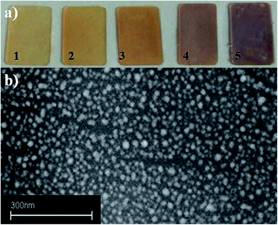 | ||
| Fig. 1 (a) Optical photograph of PDMS membranes decorated by Ag nanoparticles. The samples are obtained with several pre-polymer/curing agent weight ratio for the elastomeric substrates using different sputtering currents for the metal particles growth: #1 (3:1, 20 mA), #2 (3:1, 30 mA), #3 (3:1, 40 mA), #4 (10:1, 30 mA), #5 (20:1, 40 mA) (b) FESEM image (backscattered electrons) of sample #5. | ||
Fig. S3 (ESI†) shows some representative Ag NPs sputtered on c–Si substrates in the same synthesis conditions of the silvered PDMS membranes; the conductive substrate allowed to obtain high resolution viewgraphs and a careful analysis of the particle size and inter-particle gap dispersion. As expected, at low sputtering current (20 mA), the nanoparticles are nucleating and growing without any coalescence process, at higher current (40 mA) the nanoparticles increase their size and the coalescence increases their density shrinking the average gap between them.
As shown in Fig. 2, all the transmittance spectra of the silvered PDMS membranes are characterized by dips corresponding to plasmon resonances ascribed to enhanced absorption/scattering processes related to either LSP coupled to individual particles or yielded by inter-particles interactions. It is worth to underline that beside the NPs morphology, the effect of the dielectric substrate must be taken into account both for the LSP resonance energies and for the fields spatial localization.28,29 However, the influence of the different pre-polymer and curing agent ratios used for the synthesis of our PDMS membranes on their refractive index variation can be considered negligible.
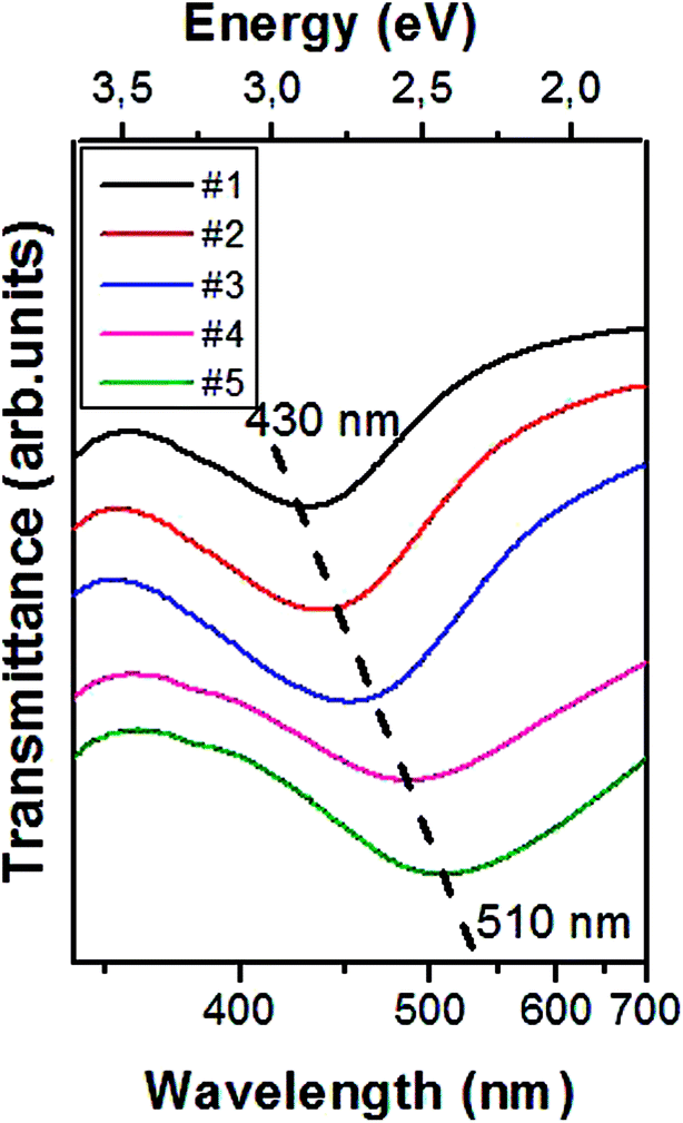 | ||
| Fig. 2 Transmittance spectra of samples obtained under different synthesis conditions; labels #1–#5 are referred to the same specimens of Fig. 1. The spectra are vertically shifted for clarity; the dashed line is a guide to the eye emphasizing the plasmonic dip positions. | ||
For densely packed NPs assembly, the major contribution to enhanced light scattering is played by the particle aggregation state. This promotes the occurrence of ‘hot spots’, where the coupling of LSP resonance within two (or more) very close NPs yields a huge concentration of the EM field.30 Molecules located at this plasmonic hot-spot can boost their Raman activity, with SERS enhancement obtainable for the smallest inter-particle gap size.31
The well-known mechanical properties of the PDMS matrix32,33 allow the control over the inter-particle gap distance through the modulation of the external uniaxial strain on the elastomer substrate. Interestingly, the plasmon resonance measured in the transmittance spectra can be tuned by applying strain to the PDMS substrate decorated with Ag NPs. Fig. 3 shows the transmittance spectra of different plasmonic substrates under several applied strains (0–50%, the percentage of the strain was calculated by measuring changes in the substrate total length before and after deformation). When comparing the transmittance spectra, we observe that each specimen is characterized by a broad plasmonic resonance, subjected to a typical blue-shift when the uniaxial strain, and consequently the average inter-particle nanogap size, are increased. This means that the main contribution to the observed plasmonic resonance can be attributed to inter-particle plasmonic interactions. This behavior is in agreement with other theoretical and experimental studies concerning with the analysis of nanoparticle dimers characterized by different nanogaps.34,35
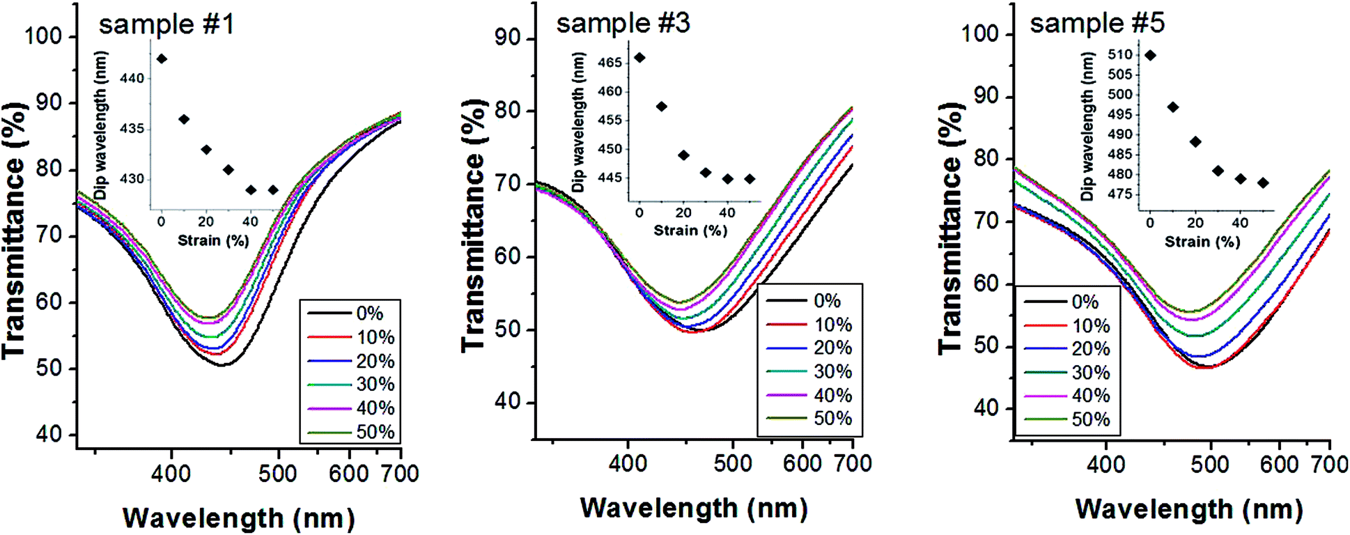 | ||
| Fig. 3 Transmittance spectra of different plasmonic substrates under external strain (0–50%). The insets show the dependence of the resonance wavelength on the applied strain. | ||
We choose to apply strains in a range 0–50% since previous experimental studies on PDMS prepared with various mixing ratios did not evidence any hysteresis behaviour.36 In fact, the plasmonic spectral shift of our membranes is found fully reversible after stretching–unstretching cycles (see Fig. S4, ESI†).
In order to get an insight on the optical response of our samples, we have developed a simple model consisting in a dimer of Ag hemispheres deposited on a PDMS substrate. The sphere diameter is 12 nm (i.e. the average size of our typical particles) and the inter-particle gap is tuned in the range d = 1–30 nm. We studied the near-field EM intensity spectra within the dimer nanogap by COMSOL Multiphysics software (3D Finite Element Method). As clearly shown in Fig. 4, the EM near-field intensity spectra (incident electric field polarized along the dimer axis) are characterized by multiple resonances. In particular, the lowest energy mode, which dominates in intensity over the higher energy modes, is subjected to a blue-shift and to an intensity quenching by increasing the inter-particle gap.
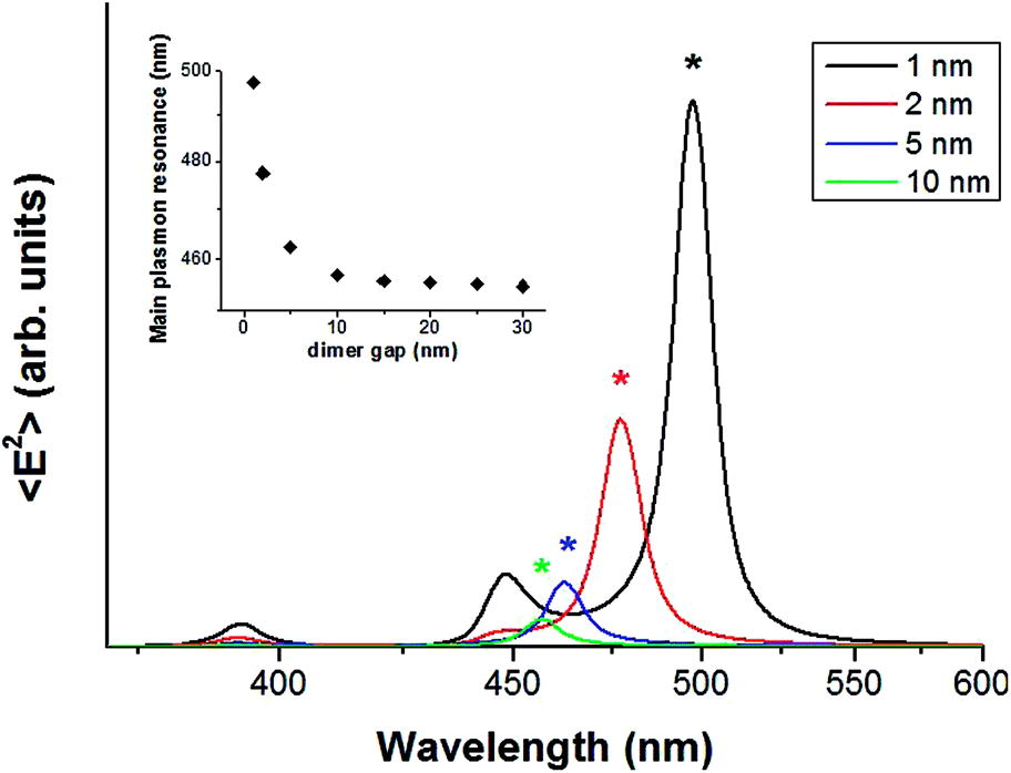 | ||
| Fig. 4 Calculated EM near-field intensity spectra within the nanogap of a dimer consisting in Ag hemispheres loaded on PDMS (sphere diameter = 12 nm). The spectra are related to different inter-particle gap (d = 1–10 nm). Incident electric field polarized along the dimer axis. Asterisks mark the stronger low-energy mode for each spectrum, whose resonance wavelength versus the dimer gap is shown in the inset (d = 1–30 nm). | ||
The multiple resonances are better evidenced in the semilogarithmic plot of Fig. 5a. Actually, for large inter-particle gaps, two resonances can be found in the visible energy range for an incident electric field polarized along the dimer axis. The lower energy mode is subjected to the above discussed blue-shift by increasing the dimer gap showing a peak splitting for d < 5 nm. On the other side, there is a higher order resonance whose energy is almost independent on the dimer separation. The phase analysis (not shown here) evidences that the lower energy mode (marked as resonance I in Fig. 5a) concerns with two coupled dipole moments oscillating in phase (symmetric mode), which can be referred as bright plasmon mode. Instead, the higher energy resonance (marked as resonance II) corresponds to an antisymmetric mode due to dark plasmons.37 The fields intensity distributions (Fig. 5b and c) show that at resonance I the EM field is enhanced and tightly localized within the dimer gap, while at resonance II the field is localized at both ends of the hemispheres, with a weak intensity. Thus, in elastic and inelastic light scattering processes the high energy mode can be neglected.
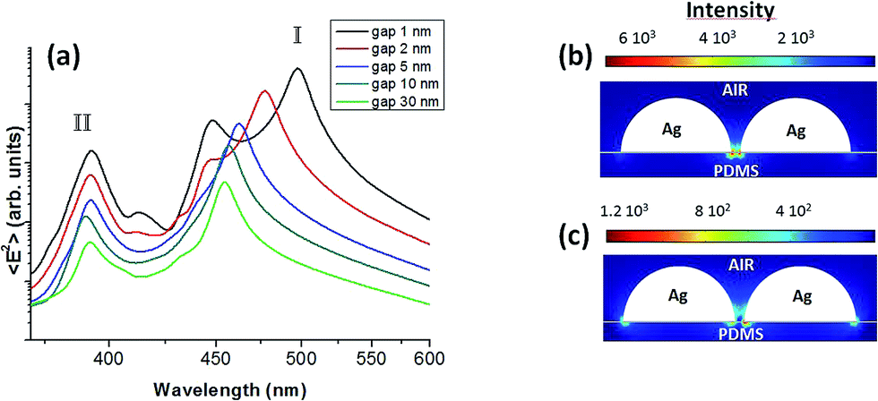 | ||
| Fig. 5 (a) Field intensity spectra of Fig. 4 shown in a semi-logarithmic plot (without any rescaling). Near field intensity distribution for inter-particle gap d = 1 nm (b) at the low-energy resonance (I) and (c) at the high-energy resonance (II). | ||
Despite the simplicity of the computational model, the results are coherent with the experimental data dealing with the unpolarized transmittance spectra discussed above. Actually, the width of the plasmonic dip featuring the transmittance measurements is much broader than the dominant peak resonance of the simulated spectra, but this can be merely attributed to the overlap of neighboring resonances due to the inter-particle gap size distribution and the polydispersity of individual particle sizes characterizing our samples.
SERS analysis of R6G
Taking into account the plasmonic tunability of the metal–elastomeric nanostructures, we checked the SERS effect by analyzing the vibrational activity of Rhodamine R6G. In particular, SERS spectroscopy performed on sample #5 excited at the substrate plasmon resonance (λLSPR ∼ 510 nm, λexc = 514.5 nm, corresponding also to the analyte electronic resonance) shows evidence of the typical Raman bands of R6G in ethanolic solution adsorbed on the substrate down to concentrations of 10−12 M (Fig. 6), among the lowest values reported in literature concerning with single molecule detection.6,38 Actually, we find 10−5 M as the minimum concentration of the experimentally detected R6G adsorbed on an homogeneous Ag thin film sputtered on PDMS under the same excitation conditions. Thus, taking as a reference such a concentration threshold for a Ag thin film, sample #5 yields an external amplified Raman efficiency (EARE)3 larger than 107.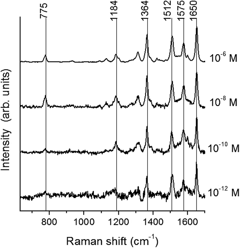 | ||
| Fig. 6 SERS spectra of R6G at several concentrations adsorbed on a Ag-coated PDMS membrane (sample #5, excitation at 514.5 nm). The main vibrational resonances are evidenced. All the spectra are normalized to the intensity of the mode at 1650 cm−1 and vertically shifted for clarity. | ||
The same SERS analyses performed on sample #1 and #3 (see Fig. S5, ESI†) show much higher limit of detections since the plasmonic off-resonance conditions (λexc = 514.5 nm, λLSPR_SAMPLE #1 ∼ 442 nm, λLSPR_SAMPLE #3 ∼ 465 nm).
Fig. 7 shows a comparison of R6G Raman spectra acquired on sample #5 using different excitation wavelengths with and without mechanical strain applied to the elastomeric membrane. For excitation at 647 nm (far both from the substrate plasmon resonance, and from the analyte electronic resonance), the Raman spectrum shows only modes related to the PDMS matrix such as CH3 symmetric and asymmetric bending at 1262 cm−1 and 1412 cm−1 respectively.39 For excitation at 514.5 nm (close to the particles plasmon/R6G electronic resonances, λLSPR = λexc), the typical RG6 vibrational modes related to xanthene and phenyl rings are easily detected at 775 cm−1 (C–H out-of plane bending), 1184 cm−1 (C–H in-plane bending in xanthene ring), 1364 cm−1, 1512 cm−1, 1575 cm−1 and 1650 cm−1 (C–C stretchings).40 The Raman signal at the same excitation wavelength is strongly quenched by stretching the substrate (50% strain). This is consistent with theoretical expectations considering the blue shift of the transmittance dip of the SERS substrate corresponding to a plasmonic off-resonance condition.
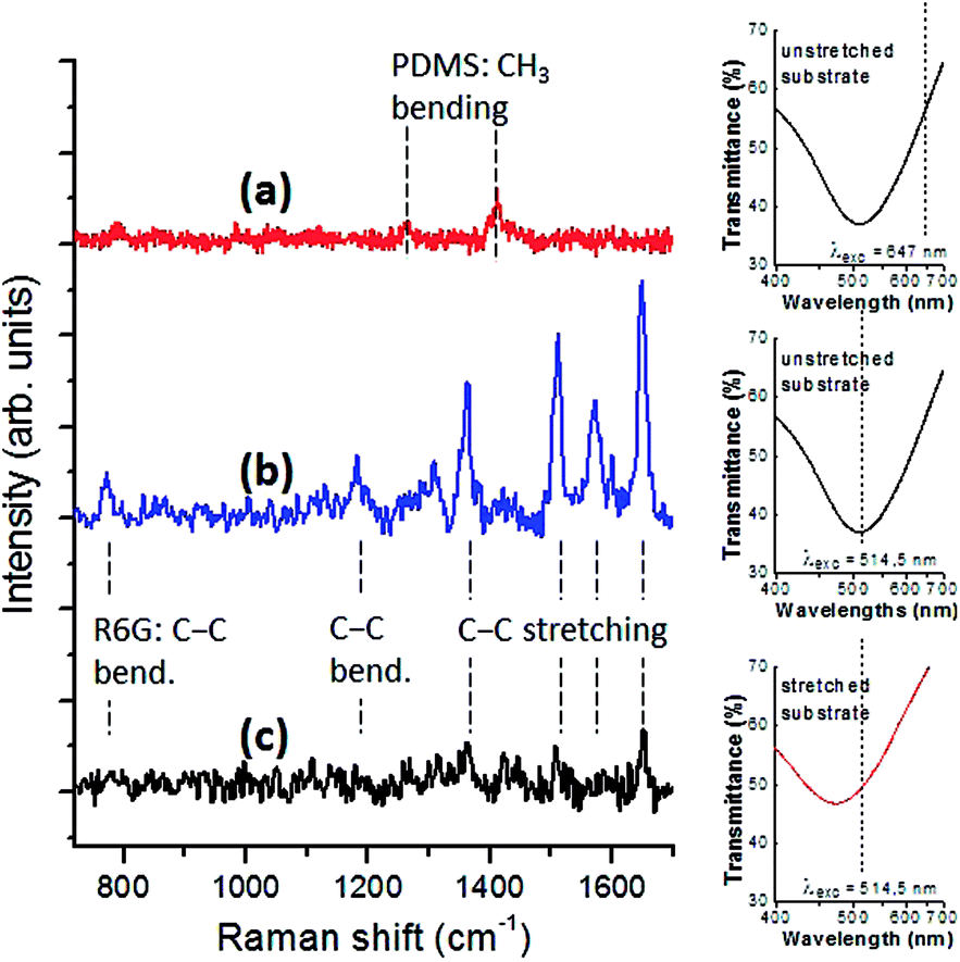 | ||
| Fig. 7 Raman spectra of R6G at a concentration of 10−8 M adsorbed on sample #5: (a) excitation at 647 nm on unstretched substrate, (b) excitation at 514.5 nm on unstretched substrate, (c) excitation at 514.5 nm on stretched substrate (50% strain). For each Raman spectrum, the plasmonic dip in the transmittance spectrum of the bare SERS substrate and the excitation wavelength are shown as a reference. | ||
SERS microfluidic device
Usually, the majority of SERS substrates are open plates where the analyte solutions are spotted and then dried producing a non-uniform molecule distribution (i.e. because of “coffee-ring” effects, where molecules likely accumulate on the edge of the liquid droplets). Thus, marked differences in spectral intensities can result for SERS detections at different positions of the open substrates. In addition, before and during the measurements, the analytes on the open chip surfaces can be easily contaminated, with deleterious consequences on the spectroscopic analysis. In this respect, microfluidic devices can solve these problems, allowing the analysis on reduced sample volumes under controlled analyte injection conditions.41Recently, Ag NPs decorated vertical nanowalls in PDMS on Silicon microfluidic devices were fabricated.42 Differently from this work, an all-PDMS microfluidic chip with a tunable active area were synthesized. The NPs are grown on the ceiling of a microchannel and then bonding on the backside another elastomeric membrane. The schematic structure of the sensor, the operating configuration and the digital photographs of the as prepared device are reported in Fig. 8.
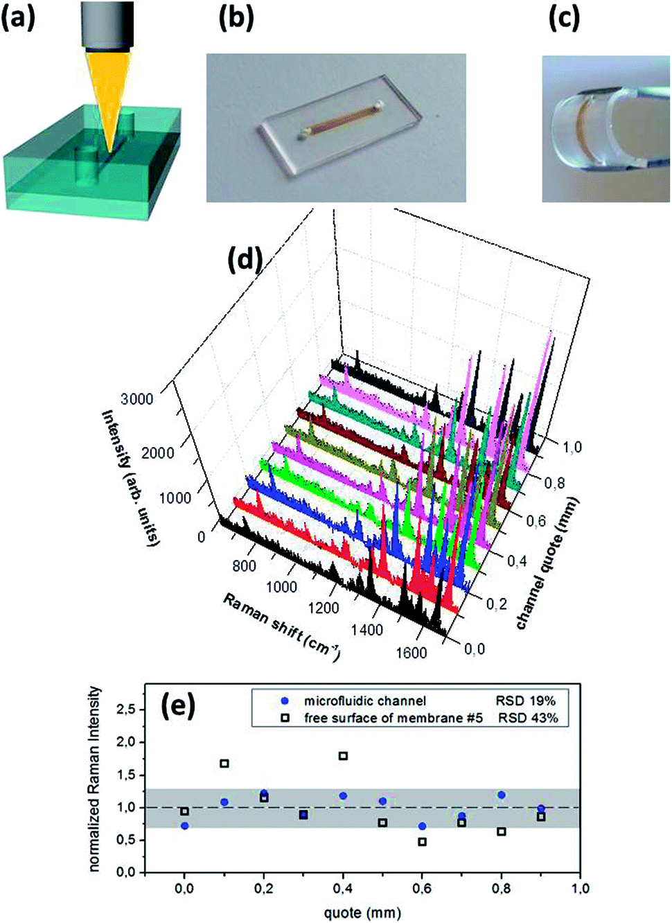 | ||
| Fig. 8 (a) Scheme of the optofluidic device, where the Ag NPs are confined in the microchannel, which can be directly probed by a focused laser beam through the objective of a micro-Raman spectrometer. (b and c) Optical photographs of the fluidic module (at rest and bended respectively). (d) Raman spectra of R6G at a concentration of 10−8 M injected in the device, probing different sites of the fluidic channel. Excitation at 514.5 nm; PDMS composition and NPs sputtering conditions are those for sample #5. (e) Comparison of the Raman intensity of the R6G mode at 1650 cm−1 (normalized to the average intensity value) over a scanning of 1 mm in the fluidic channel and on the free surface of a silvered PDMS membrane (sample #5). | ||
All-PDMS optofluidic devices have advantages over the conventional rigid substrate-based devices in their flexibility to conform to the underlying object as they can be wrapped onto curved surfaces and can be easily cut into different shapes and sizes. Moreover, like for the bare PDMS membranes, our microfluidic device shows the SERS tunability controlled by the uniaxial mechanical stretching (see Fig. S6, ESI†).
Fig. 8d shows the SERS spectra of R6G injected in the chip exciting the analyte along the channel. The collected data demonstrate a good homogeneity of the Raman signal along the microchannel, with a Raman intensity fluctuation markedly lower than the fluctuation measured on the free surface of sample #5 (relative standard deviation RSDdevice = 19% vs. RSDmembrane = 43% over 1 mm of linear scanning). This good degree of measurement repeatability is possible thanks to the microfluidic approach that allows to uniformly distribute the molecules on the Ag NPs network.
Conclusions
In summary, Ag NPs were grown by DC sputtering on PDMS slices. The noticeable flexibility of the polymeric matrix allows the application of uniaxial stress which modulates the Ag inter-particle gaps. As supported by 3D modeling, this provokes a reversible spectral shift of the plasmonic resonance making the metal–elastomer nanostructure a ‘tunable’ SERS substrate. As theoretically predicted, fixing the Raman excitation line, the vibrational signal of analytes spotted on the NPs is boosted when the excitation matches the plasmon resonance.Finally, a SERS-active substrate has been integrated in a microfluidic device, characterized by the above discussed SERS tunability, showing promising capability for highly sensitive on-chip detection.
Acknowledgements
The authors acknowledge funding from the Italian Flagship Project NANOMAX and the FIRB NEWTON, as well as stimulating discussions with Prof. Marco Sangermano (Politecnico di Torino) on physical and chemical properties of PDMS.Notes and references
- K. Kneipp, H. Kneipp, I. Itzkan, R. R. Dasari and M. S. Feld, J. Phys.: Condens. Matter, 2002, 14, R597–R624 CrossRef CAS.
- G. McNay, D. Eustace, W. E. Smith, K. Faulds and D. Graham, Appl. Spectrosc., 2011, 65, 825–837 CrossRef CAS PubMed.
- A. Virga, P. Rivolo, E. Descrovi, A. Chiolerio, G. Digregorio, F. Frascella, M. Soster, F. Bussolino, S. Marchiò, F. Geobaldo and F. Giorgis, J. Raman Spectrosc., 2012, 43, 730–736 CrossRef CAS.
- A. Bonifacio, S. Dalla Marta, R. Spizzo, S. Cervo, A. Steffan, A. Colombatti and V. Sergo, Anal. Bioanal. Chem., 2014, 406, 2355–2365 CrossRef CAS PubMed.
- S. Nie and S. R. Emory, Science, 1997, 275, 1102–1106 CrossRef CAS PubMed.
- A. Virga, P. Rivolo, F. Frascella, A. Angelini, E. Descrovi, F. Geobaldo and F. Giorgis, J. Phys. Chem. C, 2013, 117, 20139–20145 CAS.
- K. Kelly, E. Coronado, L. L. Zhao and G. C. Schatz, J. Phys. Chem. B, 2003, 107, 668–677 CrossRef CAS.
- P. K. Jain, K. S. Lee, I. H. El-Sayed and M. A. El-Sayed, J. Phys. Chem. B, 2006, 110, 7238–7248 CrossRef CAS PubMed.
- C. H. Su, P. Wu and C. S. Yeh, J. Phys. Chem. B, 2003, 107, 14240–14243 CrossRef CAS.
- L. M. Liz-Marzan, Langmuir, 2006, 22, 32–41 CrossRef CAS PubMed.
- G. Santoro, S. Yu, M. Schwartzkopf, P. Zhang, S. K. Vayalil, J. F. H. Risch, M. A. Rubhausen, M. Hernandez, C. Domingo and S. V. Roth, Appl. Phys. Lett., 2014, 104, 243107 CrossRef PubMed.
- E. Messina, E. Cavallaro, A. Cacciola, R. Saija, F. Borghese, P. Denti, B. Fazio, C. D'Andrea, P. G. Gucciardi, M. A. Iatì, M. Meneghetti, G. Compagnini, V. Amendola and O. M. Maragò, J. Phys. Chem. C, 2011, 115, 5115–5122 CAS.
- L. Gunnarsson, E. J. Bjerneld, H. Xu, S. Petronis, B. Kasemo and M. Käll, Appl. Phys. Lett., 2001, 78, 802–804 CrossRef CAS PubMed.
- Y. Y. Lin, J. D. Liao, Y. H. Ju, C. W. Chang and A. L. Shiau, Nanotechnology, 2011, 22, 185308 CrossRef PubMed.
- A. J. Haes, C. L. Haynes, A. D. McFarland, G. C. Schatz, R. P. Van Duyne and S. Zou, MRS Bull., 2005, 30, 368–375 CrossRef CAS.
- J. Yao, A. P. Le, S. K. Gray, J. S. Moore, J. A. Rogers and R. J. Nuzzo, Adv. Mater., 2010, 22, 1102–1110 CrossRef CAS PubMed.
- M. Kahraman, P. Daggumati, O. Kurtulus, E. Seker and S. Wachsmann-Hogiu, Sci. Rep., 2013, 3, 3396 Search PubMed.
- R. Alvarez-Puebla, B. Cui, J. P. Bravo-Vasquez, T. Veres and H. Fenniri, J. Phys. Chem. C, 2007, 111, 6720–6723 CAS.
- W. Lee, S. Y. Lee, R. M. Briber and O. Rabin, Adv. Funct. Mater., 2011, 21, 3424–3429 CrossRef CAS.
- H. Wang and A. Vial, J. Phys. Chem. C, 2013, 117, 24537–24542 CAS.
- C. L. Haynes and R. P. Van Duyne, J. Phys. Chem. B, 2003, 107, 7426–7433 CrossRef CAS.
- S. Olcum, A. Kocabas, G. Ertas, A. Atalar and A. Aydinli, Opt. Express, 2009, 17, 8542–8547 CrossRef CAS.
- G. Liu, Y. Li, G. Duan, J. Wang, C. Liang and W. Cai, ACS Appl. Mater. Interfaces, 2011, 4, 1–5 Search PubMed.
- H. Kang, C. J. Heo, C. J. Jeon, S. Y. Lee and S. M. Yang, ACS Appl. Mater. Interfaces, 2013, 5, 4569–4574 CAS.
- M. K. Hossain, G. R. Willmott, P. G. Etchegoin, R. J. Blaikie and J. L. Tallon, Nanoscale, 2013, 5, 8945–8950 RSC.
- A. Lamberti, M. Quaglio, A. Sacco, M. Cocuzza and C. F. Pirri, Appl. Surf. Science, 2012, 258, 9427–9431 CrossRef CAS PubMed.
- S. Srinath, R. N. Karnik and A. Majumdar, J. Microelectromech. Syst., 2005, 14, 392–399 CrossRef.
- H. Mertens, J. Verhoeven, A. Polman and F. D. Tichelaar, Appl. Phys. Lett., 2004, 85, 1317–1319 CrossRef CAS PubMed.
- A. Virga, R. Gazia, L. Pallavidino, P. Mandracci, E. Descrovi, A. Chiodoni, F. Geobaldo and F. Giorgis, Phys. Status Solidi C, 2010, 7, 1196–1199 CAS.
- J. R. Krenn, J. C. Weeber, A. Dereux, E. Bourillot and J. P. Goudonnet, Phys. Rev. B: Condens. Matter Mater. Phys., 1999, 60, 5029–5033 CrossRef CAS.
- E. C. Le Ru and P. G. Etchegoin, J. Chem. Phys., 2009, 130, 181101–181104 CrossRef CAS PubMed.
- A. Mata, A. J. Fleischman and S. Roy, Biomed. Microdevices, 2005, 7, 281–293 CrossRef CAS PubMed.
- A. Lamberti, M. Di Donato, A. Chiappone, F. Giorgis and G. Canavese, Smart Mater. Struct., 2014, 23, 105001 CrossRef.
- J. B. Lassiter, J. Aizpurua, L. I. Hernandez, D. W. Brandl, I. Romero, S. Lal, J. H. Hafner, P. Nordlander and H. J. Halas, Nano Lett., 2008, 8, 1212–1218 CrossRef CAS PubMed.
- F. Huang and J. J. Baumberg, Nano Lett., 2010, 10, 1787–1792 CrossRef CAS PubMed.
- T. K. Kim, J. K. Kim and O. C. Jeong, Microelectron. Eng., 2011, 88, 1282–1285 Search PubMed.
- P. Nordlander, C. Oubre, E. Prodan, K. Li and M. I. Stockman, Nano Lett., 2004, 4, 899–903 CrossRef CAS.
- T. Vosgrone and A. J. Meixner, ChemPhysChem, 2005, 6, 154–163 CrossRef CAS PubMed.
- S. C. Bae, H. Lee, Z. Lin and S. Granick, Langmuir, 2005, 21, 5685–5688 CrossRef CAS PubMed.
- H. Watanabe, N. Hayazawa, Y. Inouye and S. Kawata, J. Phys. Chem. B, 2005, 109, 5012–5020 CrossRef CAS PubMed.
- Q. Li, B. Li and Y. Wang, RSC Adv., 2013, 3, 13015–13026 RSC.
- J. Parisi, L. Su and Y. Lei, Lab Chip, 2013, 13, 1501–1508 RSC.
Footnote |
| † Electronic supplementary information (ESI) available: 3D schematic of the microfluidic device fabrication process, customized tensile strain device, as well as Raman spectra of R6G injected in the stretched and unstretched microfluidic device. See DOI: 10.1039/c4ra12168f |
| This journal is © The Royal Society of Chemistry 2015 |