DOI:
10.1039/C4RA11866A
(Paper)
RSC Adv., 2015,
5, 1684-1689
Synthesis of Ag–Ni core–shell nanowires and their application in anisotropic transparent conductive films†
Received
6th October 2014
, Accepted 28th November 2014
First published on 28th November 2014
Abstract
We report a modified two-step method for the synthesis of highly dispersed and conductive Ag–Ni core–shell nanowires. The conductivity of the nanowire networks was improved by thermal treatment under various atmospheres. H2-thermal treatment shows superior enhancement on electrical conductivity and reduces the sheet resistance by nearly seven orders of magnitude relative to that of the pristine networks. X-Ray photoelectron spectroscopic analysis reveals that the metallic Ni0 fraction on the surface is more important to the electrical conductivity than the amount of Ni on the surface. The transparent conductive films of Ag–Ni nanowires have a sheet resistance of 220 Ω sq−1 at a transmittance of 75%, much better than those made from the pure Ni nanowires. The Ag–Ni nanowires were aligned easily by applying an external magnetic field; the anisotropic conductivity ratio for the corresponding transparent conductive films can be larger than 105. The good performance may be attributed to the fact that the as-prepared nanowires possess moderate saturation magnetization and low coercivity, alleviating the aggregation of nanowires and favoring the nanowire alignment.
1. Introduction
Although metals possess excellent electrical conductivity in nature, they cannot be used directly as electrodes in optoelectronic products such as touch sensors, liquid crystal displays, solar cells, and organic light emitting diodes, owing to the high extinction coefficient and opaque characteristic in the visible-light region. In order to own both transparency and conductivity, indium tin oxide (ITO) is the most commonly used material in the manufacture of transparent conductive electrodes or films (TCFs). Recently, some new materials, including carbon nanotubes,1,2 graphene nanosheets,3 silver-particle grid,4 and silver nanowires (AgNWs),5,6 have been investigated widely as potential replacements for ITO in TCFs to improve the main drawbacks of ITO: inflexibility, the limited supply of indium, and poor conductivity for plastic substrates due to its inability to annealed at high-temperatures.7,8 To increase the transparency of electrodes, the candidate materials usually appear in the form of nanowires or nanotubes to create voids allowing light to pass through. Among the potential candidates, silver materials show the highest ratio of DC conductivity to optical conductivity (σDC/σOP),9 which is a key figure of merit for transparent conductive electrodes. Very recently, TCFs of AgNWs have been applied commercially in touch sensors by TPK Co.
In the AgNW films, the AgNWs are distributed randomly and disorderly. It is more difficult to assemble the nanowires into orientational structures or ordered arrays due to the occurrence of curling and twisting among the nanowires with extra-large aspect ratio. Recently, some studies have reported the aligned AgNWs could be achieved by Langmuir–Blodgett technique,10 washing process,11 polyvinylpyrrolidone (PVP) interaction,11–14 various kinds and flow directions of solvents,13 oil–water–air interface,14 and graphene oxide assistant,15 etc. Although these methods have been shown pleasing results, they are difficult to be applied in the practical manufacture process for optoelectronic devices due to the rigorous preparation conditions and the caprice of solvent evaporation. A reliable method is to apply an external force such as magnetic field to drive the nanowires into alignment. Nickel or cobalt is a ferromagnetic material and their nanowires can be aligned by applying a magnetic field, showing enhancement of mechanical properties16 and vary high anisotropic electrical behaviors.17 However, magnetic materials usually possess poor electrical conductivity, against application for TCFs. Combining with high-electrical-conductivity metals such as silver and copper, the hybrid nanowires are supposed to possess higher electrical conductivity. However, studies that describe the preparation of the bi-metal nanowires are still few in the literature. Zhang and Zeng synthesized the Cu–Ni core–shell nanowires with 200–300 nm in diameter by a one-pot synthesis method and the corresponding magnetic properties were also analyzed.18 Rathmell et al. prepared the Cu–Ni core–shell nanowires by a two-step approach to improve the limitation of the work of Zhang and Zeng (too large diameter and narrow formula window).19 The as-prepared Cu–Ni nanowires in transparent conductive films showed remarkable resistance to oxidation. McKiernan et al.20 fabricated the Ag–Ni core–shell nanowires by a two-step approach. The electrical and magnetic properties of the nanowires were further discussed. However, they found that the electrical conductivity of the hybrid nanowires was two orders of magnitude lower than that of bulk Ag or Ni. The hybrid nanowires were also exhibited superior catalytic activity for the H2 generation from ammonia borane compared to the pure Co and Ni nanoparticles.21,22
Although the aligned metal nanowires has been reported to possess excellent surface enhanced Raman spectroscopy effect,23 mechanic enhancement,16 and anisotropic electrical properties,17 to the best of our knowledge, no study has investigated high-performance anisotropic TCFs. This may be because the electrical conductivity of the pure magnetic-metal nanowires is too low or the core–shell bi-metal nanowires aren't dispersed well and entwine each other. In this study, we fabricate highly dispersed and conductive Ag–Ni core–shell nanowires by a modified two-step method. The electrical, magnetic, and surface properties of the nanowires were further investigated. The anisotropic TCFs were made from the nanowires. The anisotropic characterization of the TCFs was analyzed and discussed.
2. Experimental
2.1 Materials
Silver nitrate (AgNO3, Sigma-Aldrich), nickel nitrate (Ni(NO3)2, Showa), PVP (MW: 40![[thin space (1/6-em)]](https://www.rsc.org/images/entities/char_2009.gif) 000, Sigma-Aldrich), ethylene glycol (EG, Showa), sodium chloride (Katayama Chem.), N,N-diethylhydroxylamine (DEHA), and hydrazine (Showa) were used as received. Reagent-grade solvents and deionized water (DI water, >18 MΩ cm) were used throughout the experiments.
000, Sigma-Aldrich), ethylene glycol (EG, Showa), sodium chloride (Katayama Chem.), N,N-diethylhydroxylamine (DEHA), and hydrazine (Showa) were used as received. Reagent-grade solvents and deionized water (DI water, >18 MΩ cm) were used throughout the experiments.
2.2 Preparation of Ag–Ni core–shell nanowire
The Ag–Ni core–shell nanowires were fabricated using a two-step method, similar to the previous report,19 with preparation procedure modified to obtain more dispersible and higher-yield nanowires, which is in favor of the production of TCFs. PVP and DEHA were added into the silver nanowire EG solution synthesized as reported in our previous study (see ESI†),24,25 at final concentration of 1 wt%. 46.16 g of 2 wt% PVP, 6.88 g of 0.1 M Ni(NO3)2, and 32 g of the silver nanowire mixture were mixed and stirred at 600 rpm in a reaction vessel and heated at 120 °C by a simple straight-blade PTFE turbine under N2 atmosphere. After 5 min, 5.66 g of 35 wt% hydrazine in water was added slowly using a peristaltic pump. When the color of the solution turned from silver-whitish to black, the nickel ions were reduced to metallic nickel on the surface of AgNWs to form the Ag–Ni core–shell structure. The as-prepared core–shell nanowires were washed three times with ethanol through centrifugation and then purified using magnetic separation.
2.3 Preparation of anisotropic TCFs and thermal treatment
Glass substrates were washed with ethanol and cleaned using an O2 plasma cleaner (PDC-23 G, Harrick Plasma). The various amounts of the10 mg mL−1 Ag–Ni NW solution (listed in Table 2) was dropped and then spin-coated on a treated glass substrate of 2.5 cm × 2.5 cm (100 rpm, 5 s). Before the solution was dried, the coated substrate was placed immediately in a magnetic device with 100 mT magnetic flux density. Until the solvent was evaporated completely, the coated substrate was token out from the magnetic device for further measurement and investigation. As for the thermal treatment, the aligned nanowire films were placed in an air, N2 or H2 atmospheres at 200 °C for 20 min.
2.4 Characterization
The morphologies of the nanowires and the TCFs were examined using an optical microscope (OM, M835, M&T Optics) and a field-emission scanning electron microscope (SEM; JSM-7401F, JEOL). The core–shell structure was characterized using a high resolution transmission electron microscope (TEM; JSM 7401F, JEOL) and an X-ray diffractometer (Miniflex II, Rigaku). The elemental analysis and binding energy of the surface of the nanowires were determined by X-ray photoelectron spectroscopy (XPS) (PHI 5000 VersaProbe, ULVAC-PHI) at a take-off angle of 90°. The sheet resistances of the transparent conductive electrodes were determined using a four-pin probe meter (Loresta-GP, Mitsubishi Chemical) with an MCP-T610 probe. The transmittance and UV-Vis spectra were measured using an UV-Vis spectrophotometer (Lambda 850, PerkinElmer). The magnetic hysteresis curve for the Ag–Ni core–shell nanowires was measured using a superconducting quantum interference device magnetometer (MPMS5, Quantum Design).
3. Results and discussion
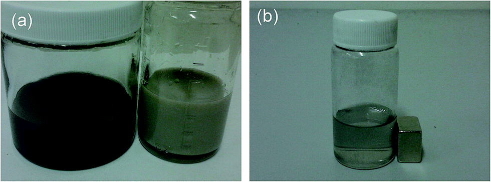
In the Ag–Ni core–shell synthesis, if the AgNWs were solved in aqueous solution with no stirring for the Ni coating reaction as reported elsewhere,19 the reaction produced a very small amount of the Ag–Ni core–shell nanowires and the nanowires were easy to aggregate. Because the AgNWs have better suspension stability in EG than water, the EG was used as solvent in our experiment. Moreover, we found that the Ni coating reaction with a non-magnetic stir would make the Ag–Ni core–shell nanowires more dispersible, less aggregate, and more productive compared to no stirring and magnetic stirring.20 The non-magnetic stirring was supposed to make the coating solution more uniform. The as-prepared Ag–Ni core–shell nanowire solution reveals a stable dispersion (Fig. 1a) and well magnetic separation (Fig. 1b).
 |
| | Fig. 1 Photo images of (a) AgNW solution (right) and Ag–Ni core–shell nanowire solution (left) and (b) magnetic separation for Ag–Ni core–shell nanowires. | |
The diameter of the pristine AgNWs is over 60–100 nm, with average diameter of ∼90 nm (Fig. 2a). After Ni coating, the diameter of the nanowires and its average increase to 140–190 and 160 nm, respectively (Fig. 2b). The surface of as-prepared Ag–Ni nanowires reveals rough and is mainly composed of nickel (Fig. 2c). According to these results, the Ag–Ni nanowires are supposed as core–shell structure and the thickness of the Ni shell can be estimated approximately to 35 nm. Fig. S1† displays the XRD patterns of AgNWs and Ag–Ni nanowires. Although the characteristic peaks of Ni corresponding to (111) and (220) planes overlap with those of Ag with respect to (111) and (311) planes, the peak at 51.7° corresponds to (200) plane, suggesting that the Ni shell is polycrystalline with a grain size of 11.4 nm calculated from the peak of (200) plane using Sherrer's equation. The surface plasmon resonance peaks of AgNWs appearing at 350 and 386 nm, corresponding respectively to the out-of-plane quadrupole resonance and the out-of-plane dipole resonance modes,26,27 are suppressed and broadened while the Ni shell is coated over the surface of AgNWs (Fig. S2†). The observation is in good agreement with the finding in Ag–Ni core–shell nanoparticles.28
 |
| | Fig. 2 SEM images of (a) AgNWs and (b) Ag–Ni core–shell nanowires and (c) TEM image of a Ag–Ni core–shell nanowire with EDS spectra recorded from its surface (indicated region). | |
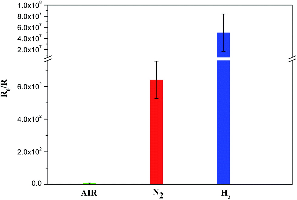
The as-prepared Ag–Ni nanowires possess poor electrical conductivity. According to the AgNW experiences, the conductivity is often able to be improved by the post-thermal treatment due to the decomposition and/or flowing of dispersants attaching to the surface of nanowires, allowing nanowires to contact tightly and fuse together and therefore reducing the junction resistance among nanowires.29 Therefore, to increase the conductivity, the Ag–Ni core–shell networks were treated thermally under various atmospheres. Fig. 3 shows the improvement on electrical conductivity by the thermal treatment; the sheet resistance reduces in the following sequence: pristine > air > N2 > H2. H2-thermal treatment shows the superior enhancement on electrical conductivity compared to air and N2 atmospheres and reduces the sheet resistance by nearly seven orders of magnitude relative to that of the pristine TCFs. To realize the cause of the enhancement, we carried out the photoelectron spectroscopic chemical analysis on the surface of Ag–Ni nanowires. Fig. 4a reveals two primary peaks in the O1s spectrum: one at near 528.8 eV is attributed to NO; the other at 530.8 eV corresponds to hydroxide species or Ni(OH)2.30,31 The intensity ratio of Ni(OH)2 to NO follows the order: pristine > air > N2 > H2, which is the same order as the reduction of sheet resistance. Fig. 4b displays two peaks at 851.8 and 855 eV in the Ni2p3/2 spectrum for metallic Ni0 and ionic-state Ni2+, respectively.32,33 N2- and H2-thermal treatments (especially H2) increase the metallic Ni0 remarkably, whereas the increase is not observed for air-thermal treatment. Table 1 shows the C, O, and Ni fractions as well as their ratios on the surface of Ag–Ni nanowires. Air-thermal treatment increases the oxygen fraction on the surface, whereas H2-thermal treatment shows the largest Ni-atom recovery. All of the thermal treatments reduce the ratios of C/Ni and O/Ni. Based on the aforementioned results, we conclude that thermal treatment may lead to the removal of hydroxyl groups or adsorbed water and the decomposition of PVP on the nanowire surface and consequently reduce the junction resistance among nanowires; N2- and H2-thermal treatments show better ability on reduction of Ni2+ to Ni0 than air one. Comparing Fig. 3 and 4 and Table 1, the valance of Ni on the surface is more important than the kinds of functional groups or Ni amount on the surface to the electrical conductivity; the metallic Ni0 faction on the surface plays a key role on the sheet resistance of TCFs of Ag–Ni core–shell nanowires. The re-oxidation is unobservable over 2 weeks after thermal annealing at room temperature. To increase the reliability, incorporating polyethoxysiloxane into the nanowire layer has been suggested to enhance the resistance to oxidation and thermal shock.25
 |
| | Fig. 3 Relative sheet resistance of the TCFs of Ag–Ni core–shell nanowires treated thermally under various atmospheres. R0 is the initial sheet resistance, and R is the sheet resistance after the thermal treatment. | |
 |
| | Fig. 4 XPS spectra of (a) O1s and (b) Ni2p3/2 for Ag–Ni core–shell nanowires under various thermal treatments. | |
Table 1 XPS analysis data for the surface of Ag–Ni core–shell nanowires
| Annealing atmosphere |
Composition, at.% |
Atomic ratio, at./at. |
| C1s |
O1s |
Ni2p |
C1s/Ni2p |
O1s/Ni2p |
| No thermal treatment |
42.70 |
38.69 |
18.61 |
2.29 |
2.08 |
| Air |
32.49 |
41.75 |
25.76 |
1.26 |
1.62 |
| N2 |
39.60 |
38.52 |
21.88 |
1.81 |
1.76 |
| H2 |
33.20 |
36.26 |
30.54 |
1.09 |
1.12 |
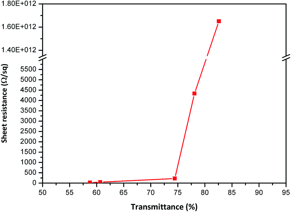
Fig. 5 presents the variation of the sheet resistance of the TCFs of Ag–Ni nanowires after thermal treatment transmittance at an incident light of 550 nm. At a transmittance of 75%, the sheet resistance of the TCFs is near 220 Ω sq−1. The performance is worse than that of the pure AgNWs.25 Roughly speaking, the Ni coating reduces the electrical conductivity by nearly 1 order of magnitude relative to that of the AgNW networks. However, our work revealed superior electrical conductivity for the Ag–Ni NWs compared to the result reported in the literature.20 We infer that the enhancement may arise from the different preparation/measurement methods and the post-thermal treatment. Nevertheless, the electrical conductivity of the Ag–Ni NWs is much better than that of the pure Ni nanowires.17
 |
| | Fig. 5 Variation of the sheet resistance of the TCFs of Ag–Ni nanowires after H2-thermal treatment as a function of transmittance at 550 nm. | |
The as-prepared Ag–Ni nanowires can be aligned easily in an applied magnetic field and show anisotropic characteristics (Fig. 6). In order to analyze the anisotropic properties, we prepared the Ag–Ni networks by a quantitative spinning method.24 As can be seen in Table 2, the anisotropic conductivity ratio (R⊥/R∥) can be larger than 105 due to the alignment of nanowires. However, the anisotropic conductivity ratio decreases with the increase of the nanowire amount. It is easy to figure out that the increase of nanowire amount will increase the probability that they touch side by side and thereby increase the conductivity in the transverse direction, resulting in the decrease of the anisotropic conductivity ratio. Nevertheless, the TCFs still have the anisotropic conductivity ratio of 1.5 when the sheet resistance of the TCFs reaches 23 Ω sq−1. Fig. 7 presents the magnetization curve of Ag–Ni nanowires. The saturation magnetization of the as-prepared Ag–Ni core–shell nanowires is 22.94 emu g−1, based on the total mass of Ag and Ni. When only the mass of Ni is considered, the saturation magnetization is calculated to the value of 35.5 emu g−1 (using the Ag core of 90 nm and the Ni shell thickness of 35 nm), which is lower than that of bulk Ni but close to that of the Ni nanoparticles (34.73 emu g−1).22 However, the coercivity of our Ag–Ni nanowires is 61 Oe, which is lower than what was reported for Ag–Ni (116 Oe)20 or Cu–Ni (237.2 Oe)18 core–shell nanowires in the literature. Moreover, remanence of our samples (3.85 emu g−1) is also lower than that reported for Cu–Ni (15.7 emu g−1).18 The reason for the lower coercivity is not cleat at present, but it may result from the fact that the Ni grain size for our samples (11.4 nm) is smaller than the Ni critical diameter (55 nm).34 The moderate saturation magnetization can avoid that Ag–Ni nanowires concentrate at the two ends of the applied magnetic field; the low coercivity and remanence can alleviate the aggregation of nanowires due to the induced magnetic force after the applied magnetic field is removed. Therefore, the as-prepared Ag–Ni nanowires are suitable for the preparation of anisotropic TCFs using an applied magnetic field. Although the resistance to oxidation.
 |
| | Fig. 6 OM image of the Ag–Ni nanowire alignment through an applied magnetic field. | |
Table 2 Anisotropic sheet resistance of the TCFs of Ag–Ni core–shell nanowires
| Amount |
R∥a, Ω sq−1 |
R⊥b, Ω sq−1 |
R⊥/R∥ |
| Sheet resistance measured in the magnetic-field direction. Sheet resistance measured in the direction perpendicular to magnetic field. |
| 50 μL |
1132 |
>108 |
>105 |
| 80 μL |
73 |
246 |
3.4 |
| 100 μL |
23 |
34 |
1.5 |
 |
| | Fig. 7 Magnetic hysteresis loop for Ag–Ni core–shell nanowires measured at 300 K. The inset is the center of the loop. | |
4. Conclusion
We have fabricated highly dispersed and conductive Ag–Ni core–shell nanowires by a modified two-step method. The nanowires with moderate saturation magnetization and low coercivity/remanence reveal a stable dispersion and well magnetic separation. The TCFs made from the nanowires show the better conductivity and transmittance than that made from the pure Ni nanowires; the sheet resistance of the TCFs can reduce as low as 220 Ω sq−1 at a transmittance of 75%. We found that the metallic Ni0 faction on the surface is more important than Ni amount on the surface to the electrical conductivity and plays a key role on the sheet resistance of TCFs of Ag–Ni core–shell nanowires. The anisotropic conductivity ratio of the anisotropic TCFs can be larger than 105. Although the ratio decreases with the increase of the nanowire amount, the TCFs still have the anisotropic conductivity ratio of 1.5 even when the sheet resistance of the TCFs reaches 23 Ω sq−1.
Acknowledgements
This study was supported financially by the Ministry of Science and Technology of the Republic of China.
References
- Z. Wu, Science, 2004, 305, 1273–1276 CrossRef CAS PubMed.
- B. T. Liu, C. H. Hsu and W. H. Wang, J. Taiwan Inst. Chem. Eng., 2012, 43, 147–152 CrossRef CAS PubMed.
- L. G. De Arco, Y. Zhang, C. W. Schlenker, K. Ryu, M. E. Thompson and C. W. Zhou, ACS Nano, 2010, 4, 2865–2873 CrossRef PubMed.
- B. Y. Ahn, D. J. Lorang and J. A. Lewis, Nanoscale, 2011, 3, 2700–2702 RSC.
- A. R. Madaria, A. Kumar, F. N. Ishikawa and C. W. Zhou, Nano Res., 2010, 3, 564–573 CrossRef CAS PubMed.
- C. H. Liu and X. Yu, Nanoscale Res. Lett., 2011, 6, 75 CrossRef PubMed.
- A. Rahy, P. Bajaj, I. H. Musselman, S. H. Hong, Y.-P. Sun and D. J. Yang, Appl. Surf. Sci., 2009, 255, 7084–7089 CrossRef CAS PubMed.
- B. T. Liu and C. H. Hsu, J. Colloid Interface Sci., 2011, 359, 423–427 CrossRef CAS PubMed.
- X. Y. Zeng, Q. K. Zhang, R. M. Yu and C. Z. Lu, Adv. Mater., 2010, 22, 4484–4488 CrossRef CAS PubMed.
- D. Whang, S. Jin, Y. Wu and C. M. Lieber, Nano Lett., 2003, 3, 1255–1259 CrossRef CAS.
- Y. P. Bi, H. Y. Hu and G. X. Lu, Chem. Commun., 2010, 46, 598–600 RSC.
- Y. Gao, P. Jiang, D. F. Liu, H. J. Yuan, X. Q. Yan, Z. P. Zhou, J. X. Wang, L. Song, L. F. Liu, W. Y. Zhou, G. Wang, C. Y. Wang and S. S. Xie, Chem. Phys. Lett., 2003, 380, 146–149 CrossRef CAS PubMed.
- P. Jiang, S. Y. Li, S. S. Xie, Y. Gao and L. Song, Chem.–Eur. J., 2004, 10, 4817–4821 CrossRef CAS PubMed.
- H. Y. Shi, B. Hu, X. C. Yu, R. L. Zhao, X. F. Ren, S. L. Liu, J. W. Liu, M. Feng, A. W. Xu and S. H. Yu, Adv. Funct. Mater., 2010, 20, 958–964 CrossRef CAS.
- Y. G. Li and Y. Y. Wu, J. Am. Chem. Soc., 2009, 131, 5851–5857 CrossRef CAS PubMed.
- K. Keshoju and L. Sun, J. Appl. Phys., 2009, 105, 023515 CrossRef PubMed.
- T. Nagai, N. Aoki, Y. Ochiai and K. Hoshino, ACS Appl. Mater. Interfaces, 2011, 3, 2341–2348 CAS.
- S. M. Zhang and H. C. Zeng, Chem. Mater., 2010, 22, 1282–1284 CrossRef CAS.
- A. R. Rathmell, M. Nguyen, M. F. Chi and B. J. Wiley, Nano Lett., 2012, 12, 3193–3199 CrossRef CAS PubMed.
- M. McKiernan, J. Zeng, S. Ferdous, S. Verhaverbeke, K. S. Leschkies, R. Gouk, C. Lazik, M. Jin, A. L. Briseno and Y. N. Xia, Small, 2010, 6, 1927–1934 CrossRef CAS PubMed.
- B. L. Sun, M. Wen, Q. S. Wu and J. Peng, Adv. Funct. Mater., 2012, 22, 2860–2866 CrossRef CAS.
- M. Wen, B. L. Sun, B. Zhou, Q. S. Wu and J. Peng, J. Mater. Chem., 2012, 22, 11988–11993 RSC.
- A. Tao, F. Kim, C. Hess, J. Goldberger, R. R. He, Y. G. Sun, Y. N. Xia and P. D. Yang, Nano Lett., 2003, 3, 1229–1233 CrossRef CAS.
- B.-T. Liu and H.-L. Kuo, Carbon, 2013, 63, 390–396 CrossRef CAS PubMed.
- B.-T. Liu and S.-X. Huang, RSC Adv., 2014, 4, 59226–59232 RSC.
- X. L. Tang, M. Tsuji, M. Nishio and P. Jiang, Bull. Chem. Soc. Jpn., 2009, 82, 1304–1312 CrossRef CAS.
- Y. Gao, P. Jiang, L. Song, L. Liu, X. Yan, Z. Zhou, D. Liu, J. Wang, H. Yuan, Z. Zhang, X. Zhao, X. Dou, W. Zhou, G. Wang and S. Xie, J. Phys. D: Appl. Phys., 2005, 38, 1061 CrossRef CAS.
- M. Tsuji, S. Hikino, M. Matsunaga, Y. Sano, T. Hashizume and H. Kawazumi, Mater. Lett., 2010, 64, 1793–1797 CrossRef CAS PubMed.
- J. Y. Lee, S. T. Connor, Y. Cui and P. Peumans, Nano Lett., 2008, 8, 689–692 CrossRef CAS PubMed.
- A. F. Carley, S. Rassias and M. W. Roberts, Surf. Sci., 1983, 135, 35–51 CrossRef CAS.
- M. C. Biesinger, B. P. Payne, L. W. M. Lau, A. Gerson and R. S. C. Smart, Surf. Interface Anal., 2009, 41, 324–332 CrossRef CAS.
- M. Alsabet, M. Grden and G. Jerkiewicz, Electrocatalysis, 2014, 5, 136–147 CrossRef CAS.
- J. L. Rodriguez, M. A. Valenzuela, H. Tiznado, T. Poznyak and E. Flores, J. Mol. Catal. A: Chem., 2014, 392, 39–49 CrossRef CAS PubMed.
- A.-H. Lu, E. L. Salabas and F. Schüth, Angew. Chem., Int. Ed., 2007, 46, 1222–1244 CrossRef CAS PubMed.
Footnote |
| † Electronic supplementary information (ESI) available. See DOI: 10.1039/c4ra11866a |
|
| This journal is © The Royal Society of Chemistry 2015 |
Click here to see how this site uses Cookies. View our privacy policy here.