
 Open Access Article
 This Open Access Article is licensed under a
 Creative Commons Attribution 3.0 Unported Licence
Synthesis and properties of molybdenum disulphide: from bulk to atomic layers
Intek Song
 ab,
Chibeom Park
ab and
Hee Cheul Choi
*ab
ab,
Chibeom Park
ab and
Hee Cheul Choi
*ab
aCenter for Artificial Low Dimensional Electronic Systems, Institute for Basic Science (IBS), 77 Cheongam-Ro, Nam-Gu, Pohang, 790-784, Korea. E-mail: choihc@postech.edu
bDepartment of Chemistry, Pohang University of Science and Technology (POSTECH), 77 Cheongam-Ro, Nam-Gu, Pohang, 790-784, Korea
First published on 15th December 2014
Abstract
Molybdenum disulphide (MoS2) has been one of the most interesting materials for scientists and engineers for a long time. While its bulk form has been in use in conventional industries as an intercalation agent and a dry lubricant for many years, its two-dimensional forms have attracted growing attention in recent years for applications in nano-electronic applications. Specifically, the single layer form of MoS2 shows significant potential as a semiconductor analogue of graphene. These exciting applications are spread over many fields, from flexible and transparent transistor devices, to low-power, high efficiency biological and chemical sensing applications. This Review Article, for the first time, provides a comprehensive overview of the synthesis, structural polytypes, properties, and applications of bulk, few layer, and single layer MoS2.
 Intek Song | Intek Song is a Ph. D. student in the Department of Chemistry at POSTECH, under the guidance of Prof. H. C. Choi. He obtained his B.S. degree in the Department of Material Science and Engineering, POSTECH in 2012. His current research topic is the development of novel methods to grow various 2D nanomaterials in large scale. He receives a Global Ph.D. Fellowship grant from Ministry of Education, Korea. |
 Chibeom Park | Chibeom Park received his B.S. in Material Science and Engineering at POSTECH in 2008 and his Ph.D. in the Department of Chemistry at POSTECH. During his Ph.D course, he spent 1 year at Cornell University as a visiting student. He is currently a postdoctoral fellow at POSTECH studying the electrical properties of chemically doped carbon-based materials under the guidance of Prof. H. C. Choi. |
 Hee Cheul Choi | Hee Cheul Choi is a Hongdeok Young Chaired Professor in the Department of Chemistry at POSTECH and Group Leader of CALDES of IBS. He obtained his Ph.D. in Chemistry from Purdue University (2001), then spent 2 years as a postdoctoral research associate at Stanford Chemistry. His work has encompassed many aspects of materials chemistry including synthesis, surface chemistry, device fabrication, and characterization of carbon-based low dimensional and quantum scale structures. |
1. Introduction
Layered crystalline materials have attracted researchers for several decades. Their unique crystallographic structure, as the term “layered” implies, is composed of separate two-dimensional (2D) layers, between which the van der Waals (vdW) interaction exists in place of ionic or covalent bonding.1,2 Therefore, most of their physical properties, such as charge carrier transport or mechanical friction, are anisotropic. Properties along the in-plane direction significantly differ from the out-of-plane counterparts.2–4 Historical applications of such structural uniqueness were confined to host lattices in intercalation chemistry5–7 or dry lubricants in mechanics.8 However, recent experimental advances have found these materials are capable of realising 2D nanomaterials, when the individual layers are isolated.9–11 These isolated single or few layers have been good topics for the fundamental research, because some of their properties are quite distinct from bulk counterparts. Researchers also expect that they have great utility in various fields, such as flexible and transparent components in nanoelectronics, active components for chemical sensors, catalysts for various electrochemical reactions, and so forth.12–14Among a variety of 2D nanomaterials, a growing number of researchers have recently focused on two-dimensional molybdenum disulphide (MoS2), as witnessed in the exponentially rising number of publications on this subject (Fig. 1). Bulk MoS2, like graphite, is a layered material, where each layer of MoS2 is composed of three-atom-thick S–Mo–S stacks (Fig. 2a). Each layer of MoS2 is often referred as a “single layer” or a “monolayer” by convention. This is contrary to other chalcogenides such as Bi2Se3, in which case it is rather called a “quintuple layer” (QL), reflecting the atomic structure of 1 QL, i.e. a stack of Se–Bi–Se–Bi–Se. Such convention, however, rarely applies to MoS2 and other transition metal dichalcogenides, such as a “triple layer,” although single-layer MoS2 or monolayer MoS2 is in fact three atoms thick. In addition, depending on the coordination of Mo atoms within a single layer and the stacking order of single layers, there are three known polytypes—namely 1T, 2H, and 3R—of MoS2.
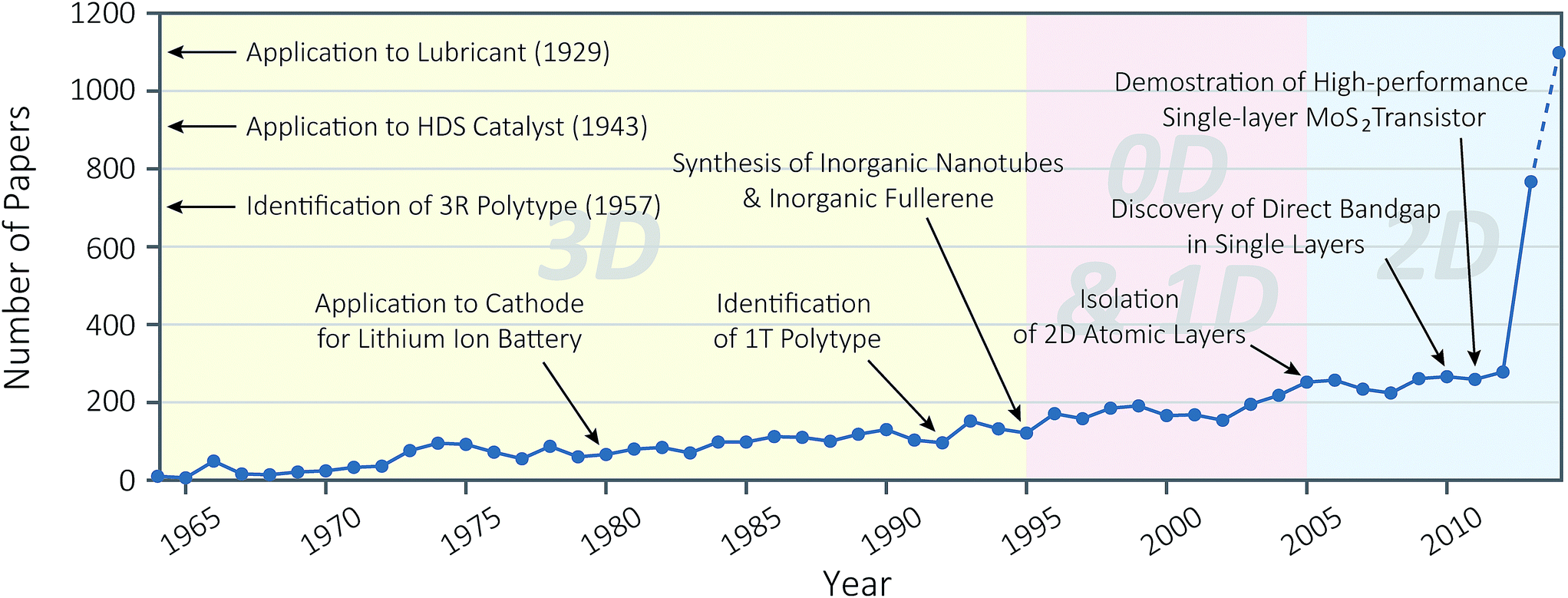 | ||
| Fig. 1 History of molybdenum disulphide research for last 50 years (1964–2014). The graph shows the annual number of journal publications, of which title, abstract or keywords contains word “molybdenum disulphide”, “molybdenum disulfide”, or “MoS2”, based on Scopus® query. Note that the number in Year 2014 (1099) is extrapolated from the number of publications till 30 September, 2014 (824). Major achievements are denoted in the graph, based on the following references: “Application to Lubricant (1929)” ref. 18; “Application to HDS Catalyst (1943)” ref. 19; “Identification of 3R Polytype (1957)” ref. 62; “Application to Cathode for Lithium Ion Battery” ref. 20; “Identification of 1T Polytype” ref. 37; “Synthesis of Inorganic Nanotubes & Inorganic Fullerene” ref. 21; “Isolation of 2D Atomic Layers” ref. 10, “Discovery of Direct Bandgap in Single Layers” ref. 25, “Demonstration of High-performance Single-layer MoS2 Transistor ” ref. 26. | ||
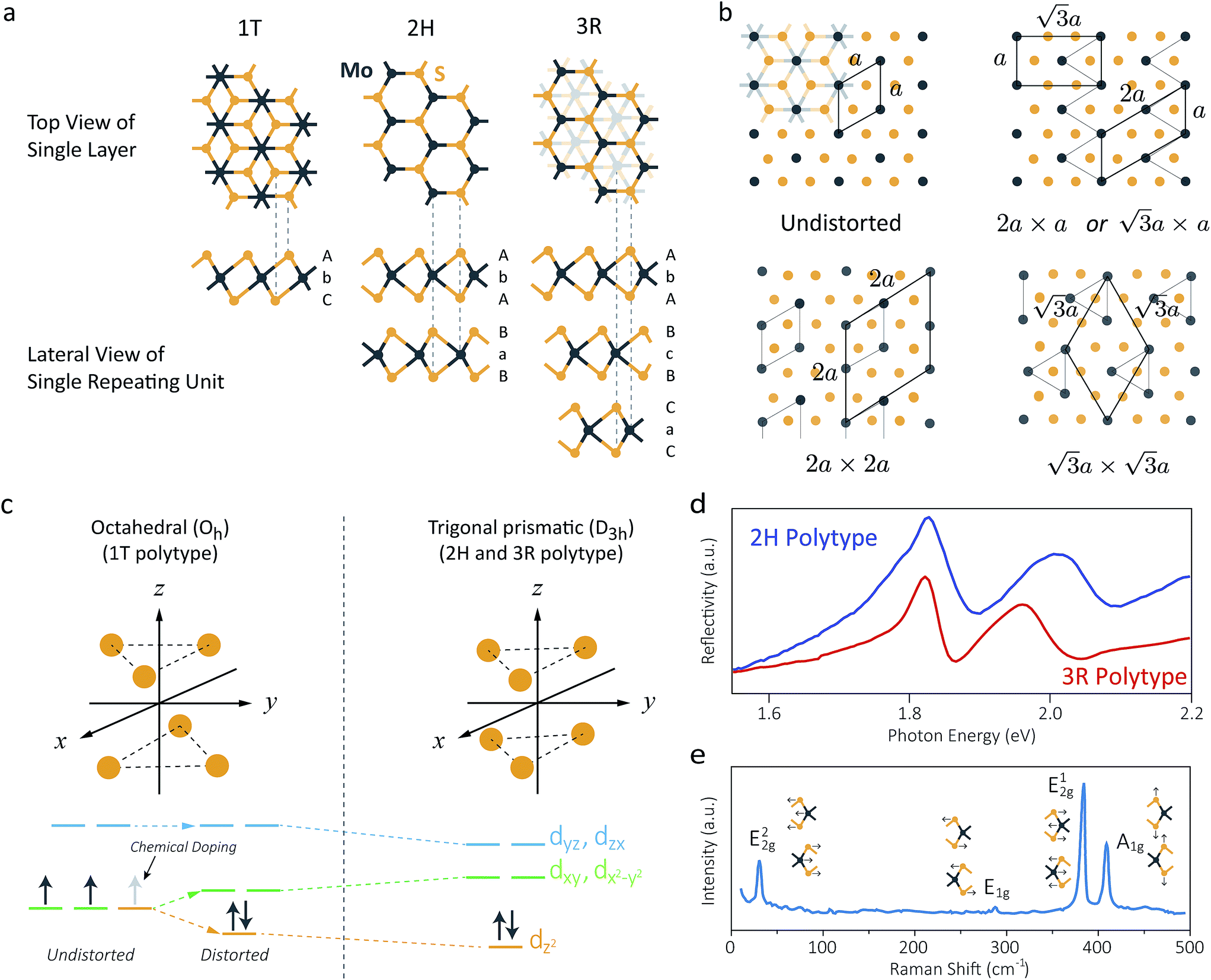 | ||
Fig. 2 (a) Schematic crystal structures of three polytypes – 1T, 2H, and 3R. The dashed lines show how the top views and the lateral views match with each other. In case of the 1T and 2H polytypes, atoms of the underlying layers exactly overlap with the layers above. However, in case of the 3R polytype, some atoms of the underlying layers do not overlap with the above layers, and thus they are shown faint in the top view. (b) Schematic illustrations of the four possible structures of 1T polytype.85 The undistorted structure is identical to the top view of the 1T polytype in (a). Other three structures show the superstructures of distorted 1T-MoS2. Chemical bondings are omitted for clarity. Thick lines illustrate the boundary of a unit cell, and thin lines show the clustering of molybdenum atoms upon distortion. Note that the 2a × a superstructure is equivalent to the  superstructure. (c) Splitting Mo 4d orbitals under octahedral (1T polytype) and trigonal prismatic ligand field (2H and 3R polytype).85 Orange coloured circles at the upper coordinates are sulphur atoms surrounding the omitted molybdenum atom at the origin of the coordinates. The colours of the orbital diagrams are unique to the orientation of the orbitals. The pale grey arrow at the orbital diagram of the undistorted octahedral ligand field shows the excess electron from doped alkali metals, which stabilises the undistorted octahedral ligand field. (d) Optical reflectivity of 2H- (blue) and 3R-MoS2 bulk (red).48 Two peaks near 1.8 eV to 2.0 eV correspond to A1 (lower energy) and B1 (higher energy) excitonic transitions. (e) Raman spectrum of bulk 2H-MoS2. The corresponding normal vibration mode of each peak is shown.51 Reproduced with permission from: (b) and (c) ref. 85 © 2002 Elsevier; (d) ref. 48 © 2014 Nature Publishing Group; (e) ref. 51 © 1986 Springer. superstructure. (c) Splitting Mo 4d orbitals under octahedral (1T polytype) and trigonal prismatic ligand field (2H and 3R polytype).85 Orange coloured circles at the upper coordinates are sulphur atoms surrounding the omitted molybdenum atom at the origin of the coordinates. The colours of the orbital diagrams are unique to the orientation of the orbitals. The pale grey arrow at the orbital diagram of the undistorted octahedral ligand field shows the excess electron from doped alkali metals, which stabilises the undistorted octahedral ligand field. (d) Optical reflectivity of 2H- (blue) and 3R-MoS2 bulk (red).48 Two peaks near 1.8 eV to 2.0 eV correspond to A1 (lower energy) and B1 (higher energy) excitonic transitions. (e) Raman spectrum of bulk 2H-MoS2. The corresponding normal vibration mode of each peak is shown.51 Reproduced with permission from: (b) and (c) ref. 85 © 2002 Elsevier; (d) ref. 48 © 2014 Nature Publishing Group; (e) ref. 51 © 1986 Springer. | ||
MoS2, especially of naturally abundant 2H polytype, has a long history of study and applications, because of its abundance in the Earth's crust.15–17 Its major industrial applications include dry lubricants,18 hydrodesulphurisation catalysts,19 and cathode materials for lithium ion batteries.20 Also, MoS2 nanotubes and fullerenes are one of the first inorganic analogues of carbon nanotubes and fullerenes to be synthesised, but their proposed applications are still restricted to traditional lubrication.21–24 However, the discovery of direct bandgap of 1.9 eV from single-layer MoS2 has opened up new possibilities of utilising MoS2 in electronics.10,13,14,25,26 This analogous form of graphene, a well-known robust semi-metal, completes the palette of 2D materials, spanning all of conductor (graphene), insulator (hexagonal boron nitride), and now semiconductor (single-layer MoS2). Furthermore, the discovery of the valley polarisation in single layers offers a novel, prospective carrier of information.27–30 Despite its indirect bandgap, two to several layers of MoS2, or “few-layer MoS2”, still have attractive properties for various electronic devices because of its semiconductivity. Various studies on single- to few-layer MoS2 have ensured its suitability for flexible, transparent, low-power devices in electronics.26 Finally, it can be utilised in important chemical applications such as hydrogen evolution reaction31,32 and chemical sensing.33
Attracted by these immense potentials, an increasing number of researchers turn their attention to explore this material. Despite such increasing popularity, there is no comprehensive review, to the best of our knowledge, concentrating on atomic layers of MoS2. Moreover most of the previous review papers on MoS2 mainly focuses on the most abundant 2H polytype only, although the 3R and 1T types have their own interesting properties. Herein, we review, for the first time, synthesis, properties and applications of 2D atomic layers of MoS2, including a concise overview of its bulk form and of its various polytypes. This review aims to provide a brief introduction of this attractive material to readers from various backgrounds in order to help them to understand and utilise this nanomaterial for their own demands. To this end, this review article is composed of following contents. The first part (Section 2) is a prelude to 2D layers, where we briefly summarise the fundamental nature and the historical application of various polytypes of bulk MoS2. The second part (Section 3) provides an up-to-date review on the studies regarding the preparation of 2D MoS2 layers by means of mechanical exfoliation, chemical exfoliation and vapour-phase growth. The third part (Section 4 and 5) describes the physical properties of 2D atomic layers, focusing on their electronic (Section 4) and optoelectronic properties (Section 5). The final part (Section 6) describes the chemical reactivity of atomic layers of MoS2, specifically in terms of their reactivity with various chemical and biological species, as well as related applications. For convenience, the term “2D MoS2” in this review stands for single- to few-layer forms of MoS2, where they have significantly different properties than the bulk form.
2. Overview on bulk MoS2
2.1 Polytypes and crystallography
As we have briefly discussed in Section 1, each layer of MoS2 is composed of S–Mo–S stacks, where a single molybdenum atom is surrounded by six sulphur atoms, as shown in Fig. 2a.2,15–17,34 MoS2 has three natural or synthetic polytypes of MoS2, which are 1T, 2H, and 3R, depending on (1) the coordination of sulphur atoms with respect to the central molybdenum atom and (2) the stacking order of each layer (Fig. 2a and Table 1).34 Here the former number denotes the number of layers within a single crystallographic unit cell, and the latter letter describes the crystallographic structure, where T stands for trigonal, H for hexagonal, and R for rhombohedral structure. For example, a unit cell of the 2H polytype contains two layers that are centrosymmetric to each other (2), creating hexagonal structure (H). Note that it is a convention to denote the polytype as the prefix to MoS2, if specified, as following: 2H-MoS2 stands for the 2H polytype of MoS2.| Polytype | Space group | Stacking order | Lattice parameters | Properties and remarks |
|---|---|---|---|---|
| 1T | P![[3 with combining macron]](https://www.rsc.org/images/entities/char_0033_0304.gif) m1 m1 |
AbC | a = 5.60 Å and c = 5.99 Å (ref. 37) | Paramagnetic. Metallic. Metastable structure (spontaneous distortion forms superstructures) |
| 2H | P63/mmc | AbA BaB | a = 3.15 Å and c = 12.30 Å (ref. 35) | Diamagnetic. Indirect band dap semiconductor (1.29 eV). The most abundant polytype in the Earth's crust |
| 3R | R3m | AbA BcB CaC | a = 3.17 Å and c = 18.38 Å (ref. 36) | Diamagnetic. Indirect bandgap semiconductor (ca. 1.29 eV). Its properties are similar to those of the 2H polytype (ref. 57) |
Of these three polytypes, only 2H-MoS2 and 3R-MoS2 are stable and found in nature (see Table 1 for a list of their properties).34–36 Both the 2H and 3R polytypes commonly have trigonal prismatic coordination (D3h) of molybdenum atoms, but they have different stacking order; 2H has stacking order of AbA BaB AbA…, while that of 3R is AbA BcB CaC AbA… Note that the upper and lower cases represent relative position of sulphur and molybdenum atoms, respectively.34 Nonetheless, both polytypes share crystallographic parameters.15,16,35,36 The distance between a Mo atom and its nearest S atom is 2.41 Å.15,35 The thickness of each layer is 3.15 Å, while the distance between adjacent layers is 3.49 Å, suggesting that the interlayer vdW interaction is weaker than intralayer covalent bonding.
In contrast, 1T-MoS2 is metastable, which is distinct from the aforementioned polytypes.37,38 It has octahedral coordination (Oh) of molybdenum atoms, and its stacking order is AbC AbC… There are three reported types of distortions in 1T-MoS2, namely 2a × 2a,  and
and 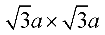 superstructures.39 The phase transformation between these superstructures is related to the intercalation and oxidation level of alkali metal during synthesis, as we described later on Section 2.3 (Fig. 2b).
2.2 The 2H and 3R polytypes with trigonal prismatic coordination
Pristine 2H-MoS2 is a diamagnetic semiconductor with indirect bandgap of 1.29 eV.25,40,41 Mo 4d orbitals are split by trigonal prismatic ligand field, and two d electrons of Mo4+ species occupy the lowest 4dz2 orbital, leading to diamagnetism and semiconductivity (Fig. 2c).42–45 Since the gap between the dz2 orbital (which mainly contributes to the valence band in the lattice) and dxy/dx2−y2 orbitals (which contributes to the conduction band in the lattice) is wide, a bandgap is formed even after the mixing with sulphur atoms occurs.40,42–46 Detailed band structure studies reveals that the momentum of the valence band maximum (VBM) is different from that of the conduction band minimum (CBM), and thus it has an indirect bandgap (the calculated band diagram is shown in Fig. 5a, and detailed discussion is given in Section 5). Therefore, the indirect bandgap leads to a negligible quantum yield for the photoluminescence (PL).25 UV-Vis absorption spectrum has two prominent peaks at 1.9 eV (λ ∼ 640 nm) and 2.1 eV (λ ∼ 580 nm), which are often referred to as the A1 and B1 exciton absorption, respectively (Fig. 2d).47,48 A detailed explanation on the origin and characteristics of these peaks are given in Section 5.1. Raman scattering has four characteristic vibration modes: the E22g mode (33 cm−1, weak), E1g mode (287 cm−1, weak), E12g mode (383 cm−1, strong) and the A1g mode (409 cm−1, strong), which is shown in Fig. 2e.49–51In terms of charge carrier transport, Hall measurements show that 2H-MoS2 is an n-type semiconductor, with charge carrier mobility of 100 cm2 V−1 s−1 at room temperature.41 However, application of high pressure (ca. 60 GPa) on 2H-MoS2 can induce a metallic state, along with change in Raman shifts due to the decrease in the interlayer distance and the change in the stacking order.52 Another viable way for semiconductor-to-metal transition is alkali metal or alkali earth metal doping, in which case metal-to-superconductor phase transition further occurs at low temperature (refer to Section 2.3).53,54 For instance, Rb-doped MoS2 (Rb0.3MoS2) has a superconducting critical temperature of 6.9 K.
2H-MoS2 is quite chemically inert. In vacuum, it is stable up to 1203 °C, at which point it turns into Mo2S3.55 It does not dissolve in most solvents, but strong oxidizing reagents such as aqua regia may oxidize and dissolve it.15,56 It also reacts with oxygen to yield MoO3 around 400 to 600 °C.
The physical and chemical properties of the 3R polytype is almost identical to those of the polytype, such as the Raman spectrum or the electronic band structure, except for minute differences in its band structure and UV-Vis absorption spectrum.16,47,48,57,58 For example, the A1 and B1 exciton absorption peaks are red-shifted by 10 meV and 62 meV respectively for 3R-MoS2, since the different stacking order alters the ionic contribution within interlayer interaction (Fig. 2d).47,57,58
These two stable polytypes of MoS2 are found in nature, and they are mostly obtained through mining. The majority (ca. 80%) of natural molybdenite has 2H stacking, and only 3% of the ore is purely 3R polytype, with the remnants exist as a mixture.59 Otherwise, they are artificially prepared through chemical synthesis, most importantly the chemical vapour transport (CVT) method, where a mixture of Mo, S, and halogen (iodine for 2H-MoS2, and chlorine for 3R-MoS2) is annealed at high temperature for several days to grow large single crystals.1,5,18,48 Selective chemical synthesis of 2H-MoS2 is achieved by (1) the direct sulfidation of elemental Mo or its compounds at elevated temperature,15,60 or (2) the pyrolysis of (NH4)2MoS4 and (NH4)2MoO2S2, which forms metastable intermediate MoS3 and MoOS2 respectively, all of which are reduced and crystallised to 2H-MoS2 upon annealing at 350 °C or higher.61 Selective synthesis of 3R-MoS2 is achieved by (1) the reaction of MoO3 and S in liquid K2CO3 at 900 °C,62 (2) the direct sulfidation of Mo under 4.7 GPa at 1050 °C,63 or (2) the transformation of 2H-MoS2 under 4 to 7.5 GPa at 1900–2000 °C.63 Note that reverse transformation takes place under vacuum at 1000 °C.64
Due to its high stability and unique layered structures, MoS2, including both the 2H and 3R polytypes, has been widely used as a dry lubricant for several decades.18,65–69 Similar to other layered materials, the in-plane friction coefficient for bulk MoS2 is much smaller (0.1) than that along c-axis (0.26).70 However, recent studies have discovered that the friction mechanism of MoS2 is distinct from other layered materials, where the lubrication of MoS2 is an intrinsic result of its inordinately weak vdW interlayer interaction.35,65,66,71,74 That is, lubrication of most layered materials requires the adsorption of vapour molecules, which can weaken the interlayer interaction.72,73 In case of some layered materials such as talc or muscovite mica, the interlayer interaction is so strong that they cannot even perform as lubricant.66,73 Therefore, most layered materials may not effectively lubricate in vacuum, where vapour molecules do not adsorb well. In contrast, friction in MoS2 decreases in vacuum, since adsorbents, especially oxidizing water, deter easy friction of weakly bound MoS2 layers.74,75 Therefore, MoS2 has been favoured as a lubricant under extreme conditions like vacuum systems or in spacecraft machinery.65,71
Another important field of industrial applications of MoS2 is the catalysis of sulphur reactions for the purpose of hydrodesulphurisation (HDS), i.e. substitution of the sulphur atom in organic molecules with a hydrogen atom.15,16,19,76,77 Usually supported on silica or alumina, MoS2 removes sulphur from various organic molecules containing sulphur such as thiophenes. Such activity specifically occurs at the rim edge of the MoS2 crystal, where sulphur vacancies easily adsorbs sulphur from the target molecule.76,78 A detailed mechanism study is given in Section 6.2.
2.3 The 1T polytype with octahedral coordination
1T-MoS2, in contrast to the 2H and 3R polytypes, is metastable, metallic and paramagnetic because of the Mo atom's octahedral coordination.37,39,79 In order to synthesise 1T-MoS2, alkali-intercalated MoS2 is hydrated and then oxidized.37,79 This reaction exploits electron donation from alkali metal to the MoS2. As shown in Fig. 2c, an excess electrons from doped alkali metal stabilises octahedral coordination as in ReS2. The subsequent oxidation process removes the excess electron, but the coordination still retains as octahedral form with slight level of distortion.79Notable consequences of the octahedral ligand field are the metallic conductivity and the metastable structure. As shown in Fig. 2c, two d electrons occupy triply degenerate d orbitals of the octahedral ligand field.38,46 Therefore, crystal distortion, similar to Jahn–Teller distortion or Fermi-surface nesting, takes place to break degeneracy and stabilise this metallic structure to some degree Equivalently, presence of excess electrons may stabilise the 1T phase, as witnessed in Re-doped nanotubes and 2D atomic layers as well.38,39,80
Since the crystal distortion takes periodically, superstructures are formed. Diffraction and STM studies have found three types of superstructures at the intermediate and the final steps of the preparation process (Fig. 2b).39,81–84 At higher level of intercalation (i.e. lower level of oxidation; KxMoS2, x ∼ 0.7 in case of KMoS2), triclinic or monoclinic structures of the 2a × 2a superstructure are found. This 2a × 2a superstructure are often found in other 1T transition metal dichalcogenides with the d3 electronic configuration, like ReS2.81,82 Further oxidation to Kx(H2O)yMoS2 (x ≤ 0.3) results in the metallic  (equivalently) superstructure, which is formed by zigzag chain-like clustering of Mo atoms.39,46 Note that this superstructure is also found in “restacked MoS2”, which is the precipitation from the aqueous dispersion of lithiated MoS2 (we described the details of the preparation method of “restacked MoS2” in Section 3.2). Further treatment of this superstructure with strong oxidising reagents such as Br2 forms the
  superstructure by trimerisation of the Mo atoms.37,39,84 However, according to theoretical calculations, this superstructure has a small bandgap, and it is even more unstable than the
 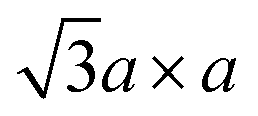 superstructure (refer to Section 4.1).
Therefore, metallic 1T-MoS2 does not have a precisely d2 electronic configuration. The 1T-MoS2 with the exactly d2 electronic configuration would instead favour the  superstructure and thus lose its metallic properties. Rather, this metallic 1T-MoS2 is equivalent to “restacked MoS2”, and it has been insufficiently oxidised to have the
  superstructure.84
Despite these distortions, 1T-MoS2 is still metastable and susceptible to the transformation to the 2H polytype. Differential scanning calorimetry (DSC) studies found that annealing up to 95 °C transforms the 1T polytype into 2H polytype. Even simple aging is enough to induce the phase transformation to 2H polytype as well.37,46,84
A well-known application of the metastable 1T polytype is as an intermediate in intercalation chemistry. A MoS2 lattice is an excellent intercalation host, because it accepts intercalates of different sizes, from small lithium ions up to macromolecules.81,85 Stable 2H-MoS2, however, does not accept most guest species directly, while 1T-MoS2 is active for the intercalation chemistry. Since lithium ion can directly intercalate into 2H-MoS2 without pre-treatment as well as convert the inert 2H polytype into the active 1T polytype, the intercalation of lithium ions, or lithiation, is done as matrix activation prior to intercalation of various guests species into inert 2H-MoS2. A notable way of lithiation is refluxing a 2H-MoS2 suspension with n-butyllithium (details are given in Section 3.2).85 An alternative way is creating an electrochemical cell comprised of Li and 2H-MoS2 as respective electrodes.86
Intercalation of other species then takes advantage of lithiation process by (1) exfoliation, where the lithiated MoS2, LiMoS2, colloid is hydrolysed to produce Lix(H2O)yMoS2 having the interlayer distance is 11.5 Å, or (2) restacking, which is treatment of LiMoS2 with an oxidising reagent or acid to obtain metallic  superstructures.39,84,85 These “activated” MoS2 can host various intercalates such as metallocene,87 metal clusters,88 or polymers.89 Intercalation of these guests often changes the properties of MoS2; for instance, intercalation of conducting polymers such as polypyrrole (PPy)89 changes n-type MoS2 into a p-type semiconductor. Intercalation of an alkali metal makes MoS2 superconducting as well (refer to Section 2.2).
One of the major applications of MoS2 intercalation chemistry is as an electrode in a lithium ion battery (LIB).20,90 A MoS2-based anode has higher specific capacity (907 mA h g−1 of reversible capacity after 50 cycles) than graphite (theoretical limit up to 372 mA h g−1), better rate capability (554 mA h g−1 for 20 cycles at 50 C rate) than Si or Ge (in case of Si, the theoretical specific capacity is 4212 mA h g−1 at the initial lithiation, but it degrades rapidly upon repetitive charge and discharge91), and significantly less volumetric expansion during lithiation (3% expansion upon full lithiation).90,92 Its energy density is comparable or higher than conventional LiCoO2.86,90 A typical problem of both MoS2 cathode and anode is their voltage, which is 2.0 V versus Li/Li+. Since this voltage value is neither high (a high value is suitable for the cathode) nor low (a low value is suitable for the anode), such intermediate value reduces the net energy density. To this end, recent efforts have focused on overcoming this obstacle by forming MoS2 nanostructures or nanocomposites, which are well reviewed in the literatures.90
3. Preparation of 2D MoS2
3.1 Mechanical exfoliation and direct visualisation
Conventional applications of MoS2, such as tribology or intercalation chemistry, are not much different from those of other layered materials. However, the isolation of single-layer MoS2 and the study on the nature of this atomically thin film have clearly distinguished this mineral from other layered materials because of its unique properties, most notably semiconductivity and valley polarisation. Preparation of 2D MoS2 is therefore the first and the most crucial step to reveal and explore its nature.The first report on single-layer MoS2 used mechanical exfoliation, i.e. repetitive cleavage of bulk crystals using adhesive tapes.10 Since molybdenite, especially 2H-MoS2, is naturally occurring mineral (refer to Section 2.2), the preparation of single crystals does not require chemical vapour transport technique as required for other TMDs.10,15,25 Thin film interference enables 2D MoS2 visualisation on thin silicon oxide layers, with the best contrast achieved on either 90 nm or 270 nm SiO2/Si substrate,93,94 which is comparable to that of graphene (90 nm and 280 nm).95 In addition, the monochromatic red channel images enhances the contrast among different numbers of layers for a 300 nm oxide layer (Fig. 3a–c).96
 | ||
| Fig. 3 (a)–(c): A mechanically exfoliated 2D MoS2 (1 to 3 layers) flake deposited on a SiO2(300 nm)/Si substrate, respectively observed by optical microscope (a), atomic force microscope (b), and optical microscope with red channels only (c).96 Inset line graphs show the contrast ((a) and (c)) and thickness profiles (b) along the white dashed line. (d) A STEM image of chemically exfoliated 2D MoS2, showing the presence of both 2H and 1T polytypes.102 The red graph shows the contrast of image along the blue line at the bottom. 2H and 1T polytypes show the different pattern of contrast, in accordance with the crystallographic structures in Fig. 2a. (e)–(g): Dispersion of 2D 2H-MoS2 atomic layers using a single solvent (e), its atomic structure measured by HRTEM (the inset shows its Fourier-transformed image) (f), and its free-standing film with thickness of ca. 50 μm (g).11 (h) A schematic illustration of electrochemical exfoliation.109 MoS2 bulk is exfoliated by the bubbles from the electrolysis of water, and the exfoliated flakes are filtered. Reproduced with permission from: (a)–(c) ref. 96 © 2012 John Wiley and Sons; (d) ref. 102 © 2012 American Chemical Society; (e)–(g) ref. 11 © 2011 American Association for the Advancement of Science; (h) ref. 109 © 2014 American Chemical Society. | ||
Despite the excellent quality of the exfoliated samples, their limited size of up to tens of micrometres and their poor thickness-control renders them apt only for fundamental research and for prototype device fabrication. While laser thinning technique can overcome the thickness variation locally,97 the development of chemical exfoliation and vapour-phase growths have been significant steps in the ultimate goal of uniform, large-scale production.
3.2 Chemical exfoliation for mass production of 2D MoS2
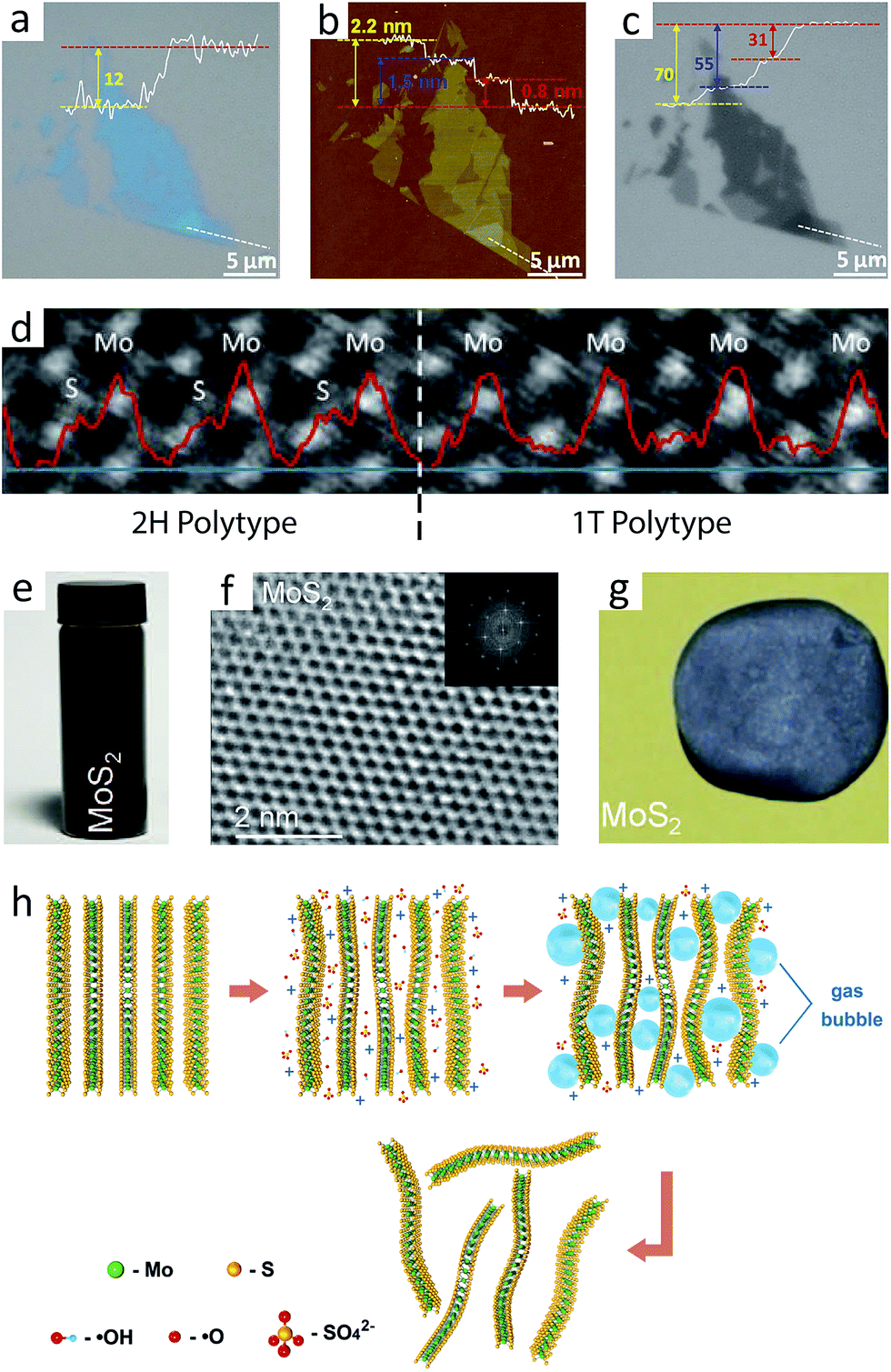
Chemical exfoliation, similar to the aforementioned mechanical exfoliation, peels off the layers of 2H-MoS2 into 2D layers dispersed in a solvent. This approach is useful for the purpose of massive production and preparation of nanocomposites.98Early studies used the restacking process to chemically exfoliate MoS2, where lithium intercalation separates layers away from each other.99–101 When MoS2 is treated with strong reducing reagents containing lithium such as n-butyllithium or LiBH4, lithium ions intercalate into MoS2 and forms LiMoS2. While pristine MoS2 shows negligible dispersibility in water, LiMoS2 disperses quite well in water, forming dispersion of 2D MoS2 flakes. The dispersed flakes can be recovered by filtration or precipitation, and the resulting product is often called “restacked MoS2”, because the layers are first exfoliated in dispersion and later “restacked” by filtration of the dispersion. A notable consequence of restacking process is the transformation of the 2H phase into the 1T phase, as mentioned in Section 2.3. A scanning transmission electron microscopy (STEM) study has revealed that resulting sheets contain both the 1T and 2H phases, forming coherent 2H/1T interface (Fig. 3d).102 In other words, the restacking process offers a facile way to synthesise two-dimensional 1T-MoS2 in large quantity, although the complete formation of the 1T polytype is not achieved.102–104 Note that this restacked MoS2 is metallic due to the formation of the  superstructure. Additional annealing process is therefore required to convert all 1T phase into the 2H phase.
In order to prepare 2D 2H-MoS2 without any 1T phase, the use of lithium should be avoided, and a number of reports used surfactants like sodium cholate instead.105,106 An aqueous dispersion of MoS2, with the proper surfactant, can be used for bioapplications such as described in Section 6.5, but in other applications remaining surfactants are often regarded as impurities.
Surfactant-free sonication of bulk crystal had problems with the stability of the exfoliated flakes, but it was recently discovered that using either certain good solvents or mixtures of poor solvents can resolve the problem; N-methyl-pyrrolidinone (NMP) and N-vinyl-pyrrolidinone (NVP) are typical examples of good solvents (Fig. 3e), while a mixture of ethanol and water is an example of the latter.11,107 The fundamental role of these solvents is to stabilise the layers of 2D MoS2 by maximizing interaction between the solvent molecules and the layers of 2D MoS2, such as London dispersion force, polar interaction or hydrogen bonding, because both types of solvents have high surface energy comparable to that of 2D MoS2 (ca. 75 mJ m−2).11,107,108 High surface energy also prevents the exfoliated flakes from agglomeration. Absent of additional surfactants, the products of these methods provide high quality 2D flakes (Fig. 3f) and can be isolated as free-standing films (Fig. 3g).
Another viable approach for larger flakes is the adaptation of interlayer bubbling by electrochemical reaction (Fig. 3h).109 The principle guiding this process is interlamellar gas bubbling, which is also used in the restacking process. Electrochemical intercalation features high selectivity toward single layers with high quality and large size. However, this method results in a slight level of oxidation damage during the exfoliation process, though it can be cured by post-exfoliation annealing.
Chemical exfoliation methods produce 2D MoS2 flakes in large quantity with the quality comparable to mechanically exfoliated ones. Demonstrably, chemically exfoliated samples show decent PL and comparable charge carrier mobility to mechanically exfoliated samples as well.110,111
This versatile approach, however, shares the same intrinsic limitations as most top-down methods; that is, it cannot produce a uniform, large-scale product on a solid substrate, since the lateral dimensions of each 2D MoS2 flake are no larger than a few tens of micrometres, even under optimised condition.108,109,112 Additionally, some of solvents may contaminate the final products, and the film obtained by evaporating solvent is essentially a collection of discrete flakes rather than continuously connected film. In order to overcome these issues, a different way of preparation, i.e. the bottom-up approach, is required.
3.3 Vapour-phase growth of large-scale 2D MoS2
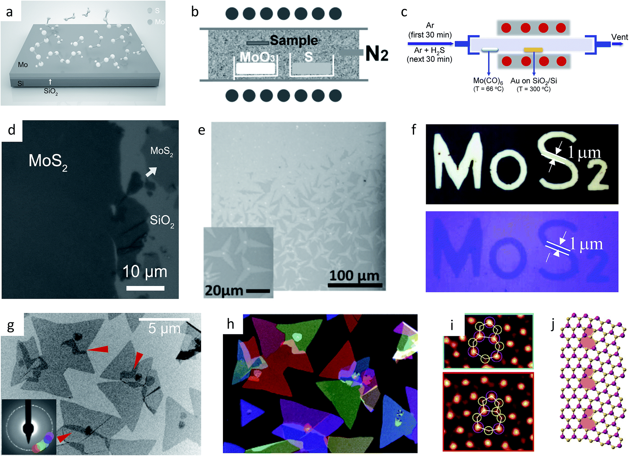
Vapour phase growth of 2D MoS2 is one of the most well-known examples of a bottom-up approach. This method enables the growth of 2D MoS2 in large scale directly on top of solid substrates by means of chemical synthesis or physical assembly from gaseous precursors. This approach ultimately aims at scalability, uniformity, and the patternability of these continuous film product. Unlike mechanically exfoliated flakes, the films grown by vapour-phase growth contain ripples and grain boundaries, thus providing an interesting environment to study their properties.113 Note that all of the processes mentioned below produce the 2H (or trigonal prismatic configuration) polytypes.Direct evaporation of MoS2 powder, i.e. vapour–solid growth, yields small flakes of high-quality single-layer MoS2 on solid substrates.30 This type of physical vapour deposition, however, cannot be used to grow large sheets of 2D MoS2, leading researchers to pursue the most promising chemical synthesis methods using molybdenum and sulphur precursors.
Early studies used evaporation of molybdenum and sulphur precursors for the preparation of 2D MoS2 on metallic substrates in a scanning tunnelling microscope (STM) chamber.114,115 These products, however, are still discontinuous nanoflakes rather than continuous films. The first genuine example of a large-scale, continuous 2D MoS2 film produced by vapour phase growth is the direct sulfidation of a pre-deposited thin molybdenum film (Fig. 4a and d).116 Although delicate control of reaction conditions yields uniform double-layer MoS2 in wafer scale117 or even vertically aligned MoS2 films,118 Stranski–Krastanov mechanism, which governs the physical deposition of the molybdenum film, hinders uniform growth over a large area.119 The preparation of molybdenum precursor film with uniformity is therefore the key issue in the synthesis of 2D MoS2 over large scale.
 | ||
| Fig. 4 (a) and (d): A schematic illustration of direct sulfidation of molybdenum film (a) and an optical image of its product (d).116 The white arrow indicates the region corresponding to single to double layers. (b) and (e): A schematic illustration of sulfidation of evaporated MoO3 (b) and an optical image of its product, triangular crystal and film (e).122 (c) and (f): A schematic illustration of surface-alloy-assisted growth (c) and optical images of patterned Au film before reaction (upper) and the corresponding patterned 2D MoS2 atomic layers transferred to a SiO2(285 nm)/Si substrate (lower) (f).128 (g) and (h): Typical MoS2 atomic layers grown by evaporation of MoO3 and subsequent sulfidation, observed by bright-field TEM (g) and the corresponding false-colour dark-field TEM image. In the dark-field TEM image, each colour shows a single grain having the diffraction pattern with the identical colour in the inset in (g). Note that red arrows indicate the overlaps of nearby crystals.129 (i) and (j): ADF-STEM images of the grain boundaries of CVD-grown polycrystalline single-layer MoS2 (i) and the schematic structure of a grain boundary of polycrystalline single-layer MoS2 (j).132 Reproduced with permission from: (a) and (d) ref. 116 © 2012 John Wiley and Sons; (b) and (e) ref. 122 © 2012 John Wiley and Sons; (c) and (f) ref. 128 © 2014 John Wiley and Sons; (g) and (h) ref. 129 © 2013 Nature Publishing Group; (i) and (j) ref. 132 © 2013 Nature Publishing Group. | ||
To this end, chemical reactions that have been used to synthesise bulk 2H-MoS2 (refer to Section 2.2) have been adapted to prepare 2D films. One example is the pyrolysis of (NH4)2MoS4. Vapour-phase injection of (NH4)2MoS4 dissolved in N,N-dimethylformamide (DMF) results in the van der Waals epitaxy of 2D MoS2 flakes on graphene.120 Upon prolonged reaction, these 2D MoS2 flakes grow and merge together to produce a rugged film. This graphene/MoS2 heterostructure, however, has limited applicability, since such semiconducting layers that are inseparable from its metallic substrate cannot be utilised for device fabrication. In contrast, dip-coating (NH4)2MoS4 on an insulating substrate resolves this problem to grow transferrable, high-crystalline three-layer MoS2.121 Although the quality is comparable to mechanically exfoliated samples, the necessity of high temperature annealing (1000 °C) and the poor controllability over the number of layers (mainly three layers, with partial two layers) are the main limitations of this two-step reaction.
Evaporation of volatile MoO3 on an arbitrary substrate followed by sulfidation process is another example that utilises bulk synthesis reaction (Fig. 4b and e).122,123 This process effectively grows MoS2 atomic layers by coalescence of triangularly shaped single crystals, which altogether results in large-scale, few-layer MoS2 displaying a high level of crystallinity (Fig. 4e). Note that a more precise control of the number of layers, including single layers, can be achieved by use of hygroscopic MoCl5 instead of MoO3,124 or sulfidation of pre-deposited inert MoO2 followed by exfoliation.125 This catalyst-free growth can be applied on arbitrary substrates, but provision of nucleation seeds by surface treatment with perylene-3,4,9,10-tetracarboxylic acid tetrapotassium salt (PTAS) enhances its versatility.126 In addition, certain substrates are known to show unique properties due to the interaction between 2D MoS2 and the substrate. Mica is such an example; since MoS2 and mica has a lattice mismatch, the single-layer MoS2 directly grown on mica has an intrinsic compressive strain.127 Therefore, the PL from this single-layer MoS2 on mica has enhanced PL intensity and suppressed PL helicity (refer to Section 5.1 and 5.2). Note that the original PL properties are recovered when the 2D MoS2 grown on mica is transferred onto a SiO2 substrate. Despite these attractive properties of the product, the process of evaporation of volatile molybdenum compound followed by sulfidation, however, lacks patternability due to random nucleation of precursor. Scalability is another limitation, since the lateral growth, which increases the size of the product, often competes with the vertical growth, which increases the number of layers, especially under prolonged reaction.
A recent paper has reported a novel route that uses surface alloy of Mo and Au as the molybdenum precursor (Fig. 4c), where the surface alloy provides uniform, atomically thin Mo layer that is confined to the surface of immiscible Au film.128 This Mo layer selectively reacts with H2S to form MoS2. This method features specific growth of atomic layers on top of Au film only, which can be easily patterned prior to reaction (Fig. 4f). However, the resulting 2D MoS2 film exhibits low carrier mobility and small grain sizes, which should be overcome.
Vapour-phase-grown 2D MoS2 exhibits various kinds of defects such as adlayers or grain boundaries (GB) (Fig. 4g and h). Adlayers on single-layer MoS2 are quite visible with optical or electron microscopy. They are found in the middle of the MoS2 flake due to the excessive growth or near the crystal edge due to overlap of neighbouring layers.129,130 These adlayers resemble double layers in terms of the structure, but they have higher conductivity than MoS2 itself owing to excess carrier density.130 In contrast, GBs are not directly visualised by optical or electron microscopy; they can be visualised by dark-field transmission electron microscopy (DF-TEM) because of the different crystal orientation of each grain.131 While certain grains may overlap with adjacent grains to form double layers, most grains coalescence and fuse with their neighbours to form an atomic boundary. Since pristine 2H-MoS2 has hexagonal rings of Mo–S–Mo–S–Mo–S (Fig. 2a), GBs exhibit chains of defective rings, such as five- and seven-membered rings or even four- and eight-membered rings along their GB (Fig. 4i and j).129,132–134 The type of GB is determined by the abundance of either sulphur or molybdenum during growth reaction as well as the angle between the grains.129,133 These grain boundaries often show electrical band structures distinct from pristine 2D MoS2, such as formation of mid-gap states, or n-doping in case of excess molybdenum atoms.133 Electrical transport across mirror grain boundaries is almost indistinguishable from that of pristine plane, but the transport across the tilted grain boundaries shows a drop in electrical conductivity.129,132,134 Theoretical calculations also predict that chains of four-membered rings from 60° grain boundary would show metallic states.133
Studying the synthesis of large-scale 2D MoS2 is important not only for the realisation of the vast potentials of 2D MoS2 but also for the related synthesis of other TMDs or heterostructures made of various 2D nanomaterials. Nonetheless, a way to synthesise single-crystalline single layers in wafer scale (i.e. larger than four inches) on arbitrary substrates is still yet to be found. In addition, the selective growth of 2D 1T-MoS2 film in large scale has still not been achieved yet; currently, lithium intercalation can only produce 1T phase in small flakes,84,103,104 and electron dosing by irradiation of electron beams can locally induce the phase transition from 2H to 1T phases in Re-doped single-layer MoS2.80
4. Charge carrier transport of 2D MoS2 and applications to transistor devices
4.1 Electronic band structure
One of the first studies on 2D 2H-MoS2 that have triggered such popularity, as shown in Fig. 1, is the discovery of semiconductivity with direct bandgap of 1.9 eV (Fig. 5a) and characterisation of prototype transistor devices.25,26,135 This was a significant discovery because such behaviour is impossible for graphene, the first 2D nanomaterial to be isolated; graphene is a native semi-metal that demands complex processes to open up a bandgap.136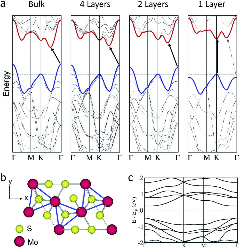 | ||
| Fig. 5 (a) Calculated electronic band structures of bulk, four-layer, two-layer, and single-layer MoS2 (from left to right).135 Black arrows indicate the fundamental transitions. The horizontal dashed lines demonstrate the energy of the highest occupied states at the K point, which becomes the VBM in single layers. As the number of layers decrease, the energy at the Γ point reduces, and it becomes lower than K point state in single layers, leading to direct gap transition. (b) and (c): The superstructure of the distorted 1T polytype single layer, showing trimerisation of Mo atoms (blue lines) (b), and the calculated bands structure of single-layer 1T-MoS2 with superstructure, showing semiconducting bandgap of 0.7 eV (c).142 Reprinted with permission from: (a) ref. 135 © 2010 American Chemical Society; (b) and (c) ref. 142 © 2014 American Physical Society. | ||
Such direct bandgap transition, which is one of the key characteristics of 2D MoS2, is attributed to the contributions of atomic orbitals to the electronic band states at different points in momentum space.25,135,137,138 As shown in Fig. 5a, the bulk form of 2H-MoS2 exhibits the indirect-gap transition from the valence band maximum (VBM) at the Γ point to the conduction band minimum (CBM) between the K point and the Γ point. The orbitals contributing to the conduction band states at the K point state are localised within the S–Mo–S sandwich, but the states at the Γ point and the CBM point have strong characters of the d orbitals of Mo and the antibonding pz orbitals of S, leading to strong dependence on vertical interlayer coupling. As the number of layers decreases, the K point state remains nearly constant, but the energy of the other states is reduced. To this end, when the number of layers is minimised (i.e. a single layer), the Γ point state in the valence band has less energy than that of the K point, and thus the K point state become the VBM. Also, the state between the K point and the Γ point, where the bulk CBM is located, has higher energy than that of the K point state in the conduction band. Therefore, single-layer 2H-MoS2 shows the direct gap transition at the K point.
Nonetheless, all of these states are still nearly degenerate in single layers, and thus a small degree of changes in the orbital overlap will alter the transition. Indeed, upon application of tensile stress the fundamental transition in single layers becomes indirect bandgap transition between Γ and K points.139–141
Electronic properties of the 1T single layer are unique in that they are predicted to display a bandgap opening of 0.7 eV (Fig. 5c) due to distortion from centrosymmetric (ideal) structure to trimerisation of molybdenum atoms having the  superstructure (Fig. 5b).142 Such trimerisation has been predicted and observed in bulk layers as well (refer to Section 2.3). Berry phase calculation shows that the distorted structure results in spontaneous polarisation along the z axis, while the in-plane polarisation vanishes. The coercive electric field required for switching the sign of polarisation domain is estimated to be 107 V cm−1, which is easily achieved by a field-effect transistor (FET) device. That is, if this phase can be stabilised, single-layer 1T-MoS2 is an excellent candidate for the thinnest ferroelectric device ever.
4.2 Charge carrier transport properties
In order to take full advantage of semiconducting properties of 2D 2H-MoS2, in-depth studies on its semiconducting nature and properties is the first step, and a number of charge transport studies have been carried out so far.A typical back-gated FET with single-layers MoS2 as channel shows charge carrier mobility of 0.5 to 3 cm2 V−1 s−1 at room temperature with n-type semiconductivity.10 Introduction of an additional top gate with high-κ dielectric material such as HfO2, as shown in Fig. 6a, may enhance the charge carrier mobility and transport characteristics (Fig. 6b).26,143–146 Such an effect is also valid for few-layer MoS2 FET, stating that in spite of its indirect bandgap, few-layer MoS2 is still an attractive semiconductor material.147
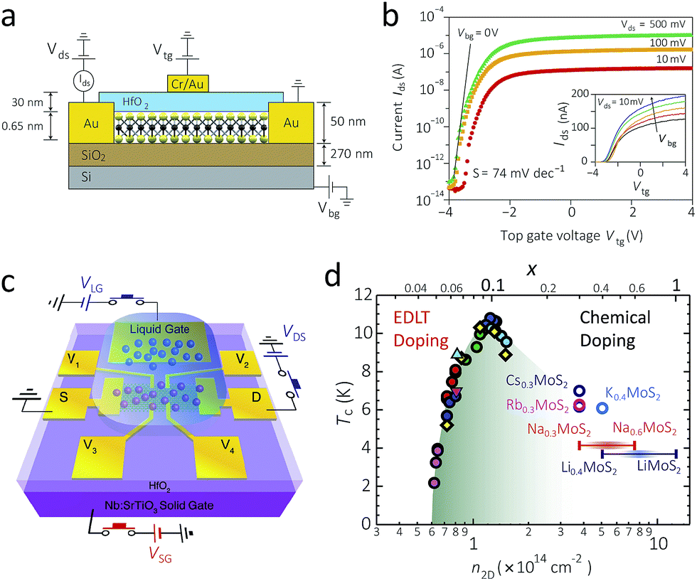 | ||
| Fig. 6 (a) and (b): A schematic illustration of a 2D MoS2 FET device with both the back gate (SiO2) and the top gate (HfO2) (a), and its transfer characteristics with the varying top-gate voltage (b).26 Since the increase in the top gate voltage makes more current flow, it is an n-type semiconductor. The inset in (b) shows that the increasing back-gate voltage also increases the electric current. (c) A schematic illustration of an EDLT with an ionic liquid gate. Here the transparent blue droplet shows the ionic liquid, which is located between the channel at the centre and the gate electrode at the top.157 (d) The phase diagram of the superconductor critical temperature versus the charge carrier concentration. The green area, which looks like a dome, represents the superconducting state. The marks at the left half shows the data obtained by EDLT doping, and those at the right half shows that of chemical doping by alkali metal.157 Reproduced with permission from: (a) and (b) ref. 26 © 2011 Nature Publishing Group; (c) and (d) ref. 157 © 2012 American Association for the Advancement of Science. | ||
Chemical doping is often an effective way to modulate electric transport properties in semiconductors. In general, the charge carrier mobility in 2D MoS2 is robust against ionic doping; to induce a significant effect, the required carrier density is at least 5 × 1011 cm−2.146 Higher doping of Nb, a well-known p-type dopant for MoS2 bulk-,41 fullerene-,148 and nanotube149-type of MoS2, turns 2D MoS2 into p-type semiconductor with hole mobility of 8.5 cm2 V−1 s−1.150 Au is another example of p-dopants,151 which results in p-type transport from surface-alloy assisted growth.128 Re is an n-type dopant for MoS2 fullerene and nanotubes,152 but theoretical study predicts that it may not be effective for 2D layers.153 Alkali metal is a better option; exposure of FET device into K vapour results in electron concentration up to 1 × 1013 cm2.153,154 It was also shown that the Na impurities or the O dangling bonds from a SiO2 substrate can become n-type and p-type dopants, respectively.155
Electrical doping provides a reversible way to modulate the charge carrier transport properties of 2D MoS2. While a mild level of electrical doping induces the gate effect just as in typical semiconductors, a higher level of doping, with charge carrier density more than 1 × 1013 cm2, induces semiconductor-to-metal transition due to electron–electron interactions.156
A more extreme case of electrical doping by the electric double-layer transistor (EDLT) device with an ionic liquid gate (Fig. 6c) induces switchable, native superconductivity, i.e. without chemical doping (refer to Section 2.2).157,158 Fabrication of prototype devices demonstrates that the critical temperature of superconductivity can reach up to 10.8 K upon optimal electric doping, which is the highest value among all TMD materials. A combined study of both chemical doping and electrical doping shows that the superconducting state appears within a specific “dome-like” range of the temperature and the charge carrier density, where the critical temperature is maximised at carrier density of 1.2 × 1014 cm−2 (Fig. 6d).157
4.3 Toward fabrication of high-performance atomically thin FET
In order to fully exploit the aforementioned properties, it is essential to optimise the FET fabrication conditions are crucial as well. Typical electrode materials for 2D MoS2 FET are Au (work function = 5.0 eV) and Ti (work function = 4.3 eV); Ti is a better option for Ohmic-like contact, since its work function is comparable to MoS2 (electron affinity = 4.0 eV), and Ti has a smaller lattice mismatch (by 1%) with MoS2.26,159 A more comprehensive study shows that an even better option is rare Sc (work function = 3.5 eV).160 Mo is another option, where the contact region becomes metallic, resulting in a small Schottky barrier of 0.1 eV.161In terms of gate dielectrics, the fabrication of an FET device with both the bottom and top gates can enhance the 2D MoS2 FET performance, leading to a high mobility of almost 15 to 55 cm2 V−1 s−1, an on–off ratio more than 1010, and a sub-threshold swing reaching down to 60 mV per decade at an extremely short channel (Fig. 6b).26,144,145,162 Note that special cares should be taken for the calculation of the mobility value of such dual-gate devices, since the capacity of the gate dielectrics may be underestimated, which results in the overestimation of the charge carrier mobility value.41,144,145 Such performance enhancement by dual gate fabrication is attributed to suppressed charged-impurity scattering, in accordance with theoretical calculations.143,145,156 In addition, the use of HfO2 is also favoured over Al2O3 in flexible devices, because it features slow crack propagation and robust charge carrier mobility against bending.163
Special modification of device components further demonstrates novel properties of 2D MoS2. For instance, the introduction of the previously mentioned EDLT device with an ionic liquid gate, which enables extremely high doping (∼1 × 1014 cm2), can establish a p-type conducting state, leading to ambipolar behaviour of few-layer MoS2.164 Using PMMA as gate dielectric and capping material can further enhance charge carrier mobility.165 Also, applying different bias between source-gate and drain-gate in the EDLT device with an ionic liquid gate allows for a stable p–n junction within a single crystal of MoS2, when the temperature is changed from 220 K to 180 K while the gate voltage is applied.166 This phenomenon is based on cooling across the glass transition temperature of the ionic liquid with simultaneous gating, where the motion of the ions of the ionic liquid couples with the accumulation of charges. Incorporation with light illumination or adsorption of small molecules can further tune transistor operation, suggesting utilisation as a phototransistor or a gas sensor, as described in Section 5.4 and 6.1, respectively.
Although the relatively low charge carrier mobility of 2D MoS2 discourages direct competition with III–V semiconductors, 2D MoS2 transistor devices show high on–off ratios and low stand-by power, which suggests suitable application for low-power electronics.162 As a proof of concept, a group of single-layer MoS2 transistors have successfully demonstrated logic gate operations, which are the key functionality required for the fabrication of complex processing units.167
5. Optical behaviours of 2D MoS2 and applications to optoelectronic devices
5.1 Absorption and emission characteristics of 2D MoS2
Direct bandgap makes the optoelectronics of single layer 2H-MoS2 exceptional among all types of MoS2. The reflectance difference spectrum has two prominent peaks at 670 nm (A1) and 627 nm (B1), similar to the bulk form, but it shows strong emission corresponding to these absorption peaks (Fig. 7a), with quantum yield of 4 × 10⁻³, which is four orders of magnitude higher than that of the bulk.25,135 These emissions are in fact PL generated from direct bandgap transition. Double-layer MoS2 shows one PL peaks at 1.59 eV (ca. 780 nm) and two peaks near 1.88 eV (ca. 660 nm), with quantum yield around 10−5 to 10−6.25 These peaks shift with the increasing number of layers, where the first peak at 1.59 eV continuously approaches to indirect bandgap of 1.2 eV in the bulk. Band structure studies show that the first peak is indirect-gap luminescence, while the others are direct gap hot luminescence, i.e. the reverse process of the A1 and B1 excitonic absorption.25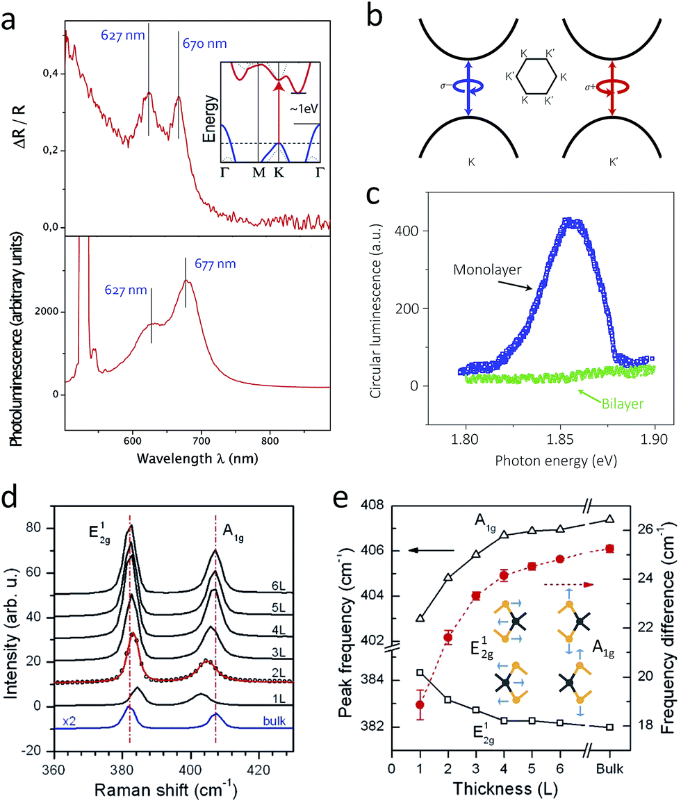 | ||
| Fig. 7 (a) A reflectance difference (upper) and photoluminescence spectrum (lower) of single-layer MoS2. The inset in the upper graph describes the band structure of bulk MoS, having indirect bandgap2.135 (b) and (c): A schematic band diagram showing the origin of valley polarisation (b) and unique circular dichroism of photoluminescence from single layer at 10 K under circularly polarised illumination (c).28 (d) and (e): Raman spectra of MoS2 with different numbers of layers (d) and shift of Raman vibration modes with respect to the different number of layers (e). The inset in (e) depicts corresponding normal vibration modes.173 Reproduced with permission from: (a) ref. 135 © 2010 American Chemical Society; (b) and (c) ref. 28 © 2012 Nature Publishing Group; (d) and (e) ref. 173 © 2010 American Chemical Society. | ||
The splitting of the A1 and B1 peaks is mainly attributed to the splitting of the VBM at the K point, which has different origins in the single layer case and the multilayer case.168 On the one hand, splitting of the VBM in single layer is purely attributed to spin–orbit coupling because of the lack of inversion symmetry. On the other hand, splitting in multilayers, which do possess inversion symmetry, is due to a combination of both spin–orbit coupling and interlayer coupling.
Since absorption and emission profiles are closely related to the band structure, modification of the band structure may change the intensity and energy of the PL peaks. For instance, electrochemical intercalation of alkali metal ions can reversibly quench PL in 2D 2H-MoS2, because it induces the phase transformation to the metallic 1T phase.169 Also, the application of strain reduces the intensity and energy of A1 exciton peak, since the strain will reduce the direct gap at K point, as discussed in Section 4.1.139–141 Note that the strain required for direct-to-indirect gap transition in optical bandgap is much less than that of the electrical bandgap due to the large exciton binding energy.
5.2 Unique valley polarisation and trion formation
A notable feature of PL from single-layer MoS2 is valley polarisation, where the PL conserves the circular dichroism of the incident light. The unique phenomenon is the results of spin–orbit coupling together with the absence of inversion symmetry.27–29 Single-layer MoS2 has six CBMs and VBMs, which are referred as “valleys”, at the K points (refer to Section 4.1). Spin–obit coupling further splits each valley into different spins (refer to Section 5.1), and circularly polarised light excites opposite spins at the K and K′ valleys located at the opposite positions in k-space (Fig. 7b). Here, because of time reversal symmetry, single layer MoS2, which lacks inversion symmetry, does not allow inter-valley transition. This spin-selective population at opposite valleys is preserved upon the polarised illumination, and thus PL maintains the same circular dichroism as the incident light (Fig. 7c). Since this phenomenon requires the broken inversion symmetry and the spin–orbit coupling at the same time, even double-layer 2H MoS2 does not show valley polarisation. However, the 3R polytype shows valley polarisation regardless of the number of layers, since the structure inherently lacks inversion centres.48 Note that illuminating a single-layer MoS2 transistor with circularly polarised light results in valley Hall effect, where Hall voltage occurs due to valley polarisation.170Another unique feature of the optoelectronics of single-layer MoS2 is the formation of a negative trion, a quasiparticle comprised of two electrons and one hole, upon illumination.171 Such phenomenon is absent in other conventional direct-gap semiconductors, where illumination only creates an exciton, a pair of an electron and a hole. Gate-voltage-dependent absorption and PL studies reveal the existence of two components in both PL and A1 exciton absorption in single-layer MoS2. The intensity of the higher energy component diminishes upon electron doping, but the other component largely retains its intensity regardless of the applied gate voltage. Here the former is attributed to the formation of neutral excitons, while the latter is related to trions, which are created by binding of electrons to pre-existing electron–hole pairs. Its binding energy is large enough (20 meV) to manifest at room temperature as well. One of the direct results of trions is the effect of chemical doping on the intensity of PL; for instance, p-type dopants like tetracyanoquinodimethane (TCNQ) enhance the PL intensity, because it promotes recombination of excitons rather than trions.172
5.3 Raman spectroscopy and phonon–photon interaction
Phonon–photon interaction of 2D MoS2 features the shift of vibration energy upon the decreasing number of layers. Of the four major Raman-active vibration modes, out-of-plane (or equally A′1 mode in single layers, concerning their different symmetry from the bulk) and in-plane (or equally E′ mode in single layers) exhibit notable shifts.173 The A1g vibration mode experiences softening, since interlayer coupling is weakened upon the decreasing number of layers. In contrast, the E12g vibration mode shows anomalous stiffening, which is attributed to the stronger dielectric screening of the long-range Coulombic interaction with the decreasing number of layers.174 To this end, in single-layer MoS2, the A1g vibration appears near 404 cm−1 (cf. 408 cm−1 for bulk), and the E12g mode is near 385 cm−1 (cf. 383 cm−1 for bulk), regardless of the wavelength of the incident laser (Fig. 7d).173,175 Therefore, the energy difference between them is often a facile indicator of the number of layers (Fig. 7e).In addition, the position of each vibration mode with respect to the zero-strain reference reflects the amount of applied strain.139–141 While the out-of-plane A1g mode is robust against tensile strain, the in-plane E12g mode significantly changes. At low strain, the in-plane E12g vibration mode is softened, and thus the corresponding peak in Raman spectrum is red-shift and slightly broadened. However, at higher strain, the crystal symmetry is apparently changed, and thus the double degeneracy of the E12g vibration mode is lifted, leading the splitting into two peaks in the Raman spectrum.
The aforementioned peaks are first-order Raman peaks, which are commonly found regardless of the wavelength of incident laser.175 However, 325 nm laser reveals additional resonant Raman spectrum within the range of 750 to 840 cm−1.176 These peaks are attributed to spin–orbit splitting at the valence band, specifically because of electron-two-photon triple resonance via Fröhlich-interaction and deformation potential. Note that the energies of these peaks do not depend on the number of layers. Also, 633 nm laser induces resonant Raman peaks such as 2LA (M) peaks near 440 cm−1 in thicker MoS2.175
5.4 Application to optoelectric device
The direct bandgap of single-layer MoS2 results in unique photon–electron interaction. Therefore, characterisation of FET devices under external illumination offers a versatile way to assess the optoelectric nature of 2D MoS2. When light with lower energy than the direct bandgap illuminates the interface between an electrode and 2D MoS2, it shows photothermoelectric effect.177 This is unique among semiconductors in that other materials do not flow photocurrent upon sub-bandgap illumination. This is attributed to the large mismatch of Seebeck coefficients between the electrodes and the single-layer MoS2, with values ranging from −4 × 10² to −1 × 10⁵ μV K−1 depending on the gate voltage.Upon super-bandgap illumination, single-layer MoS2 phototransistors show photoresponsivity of 7.5 mA W−1 up to 880 A W−1 for optimised device geometry, on–off ratio of 103 and switching time of 50 ms.178,179 Ultrahigh photoresponsivity is six orders of magnitude higher than that of graphene, because the existence of a bandgap hinders the exciton recombination. Moreover, it is sensitive to most of the visible light because of its direct bandgap, and its noise-equivalent power is 1.8 × 10⁻¹⁵ W Hz−1/2, which is an order less (better) than commercial silicon avalanche photodiodes. Such application is also demonstrated for vapour-phase-grown MoS2, in which case the photoresponsivity is up to 2200 A W−1 and the time constant is down to 55 ms.180 Bandgap modulation by thickness control results in tuning of the photoresistivity wavelength; for example, single-layer and double-layer MoS2 are sensitive to green light, and triple-layer MoS2 is sensitive to red light.181
Based on the photon–electron interaction discussed above, 2D MoS2 can be also incorporated into photovoltaic cells as the active layer in a heterojunction solar cell182 or as a hole-extraction layer.183 The former (ref. 182) has a structure of Al/2D MoS2/p-type Si/Ag, where n-type MoS2 and p-type Si form type-II heterojunction. Its photoconversion efficiency is 5.23%, which is the highest among all single-layer TMD-based solar cells. In case of the latter (ref. 183), its band structure, chemical stability and lack of dangling bonds make 2D MoS2 suitable for photovoltaic cell operation, and it shows power conversion efficiency of 8.11%, which is superior to the previously reported MoO3 counterpart.
Electroluminescence is another fundamental optoelectric operation of direct bandgap semiconductors, which is required for light emitting devices. Electroluminescence of 2D MoS2 is demonstrated using hot carrier process at a Schottky barrier.184 This hot carrier process occurs when excited electrons are injected into the conduction band through the Schottky barrier, where significant band bending generates excitons. These excitons are recombined through a radiative process, which enables electroluminescence without the formation of a p–n junction. This electroluminescence has prominent A1 excitonic characteristics (at 685 nm) only, because B1 excitonic states are not populated upon electric bias. Pristine MoS2, however, still requires higher quantum yield for practical application, and this is expected to be achieved by formation of heterostructures.
Based on these novel electronic and optoelectronic properties, 2D MoS2 is now one of the most promising materials for flexible, transparent electronic device components. For instance, an AFM study has proved its substantially high mechanical stiffness (Young's modulus of 270 ± 100 GPa, and breaking stress of 22 ± 4 GPa). That is, it is flexible enough to be used with polyimide (PI) or polydimethylsiloxane (PDMS) substrate, which is one of the most frequently used substrates for flexible electronics.185,186
6. Molecular and biomolecular interactions of 2D MoS2
6.1 Application to molecular and biomolecular sensors
The study of the interaction between 2D MoS2 and other molecules often utilise FET devices, especially in case of the semiconducting 2H polytype, because these devices offer an appropriate environment to control and assess electron transport upon chemical modification of 2D MoS2. That is, reversible adsorption of various moieties on 2D MoS2 often changes its properties as well as the properties of the target molecules. Detection of such changes open up the possibility of developing 2D MoS2 based sensors. In addition, flexibility, transparency, economic massive production, and high sensitivity are major advantages of 2D MoS2 over other bulk or other nanomaterials, even including graphene and other 2D nanomaterials.11,33,98,187One such example is as an active sensing component for chemical and biomolecular sensors. Adsorption of target molecules changes the charge transport properties of the 2D MoS2 FET device, so the electric conductivity correspondingly changes upon exposure. One of the first demonstrations is a NO gas sensor.33 This device shows remarkable detection power, with a detection limit which reaches down to 0.8 ppm and a high signal-to-noise ratio (Fig. 8a). A more comprehensive study shows that other molecules like NO2, NH3, and H2O are well detected, and its detection power can be further enhanced by the incorporation of gate effect or light illumination.188 For example, a moderate level of illumination of green light significantly enhances the detection sensitivity of NO2. A larger number of layers is favoured for better gas detection, since thicker samples have higher charge carrier concentration and higher on/off ratio. A first-principle calculation study has shown that this change of current is caused by the charge transfer from the adsorbent gas to the 2D MoS2 film.188,189 Upon adsorption of the gas molecules, the Fermi level of 2D MoS2 changes without significant changes in the band structure due to charge transfer. In addition, most of the gas molecules, including NO,33 are charge acceptors, which turns 2D MoS2 into p-type semiconductor, and NH3 is shown to be a charge donor.
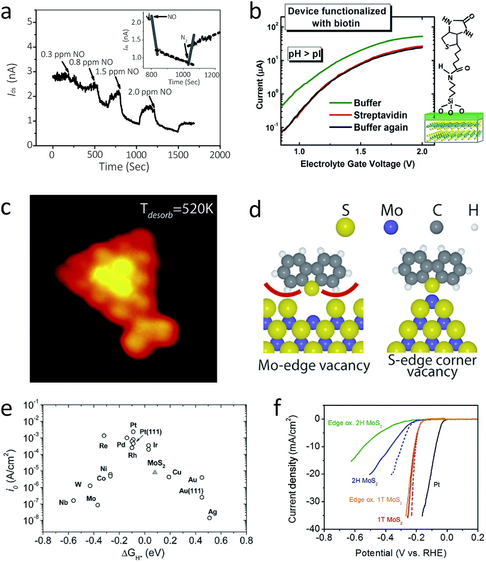 | ||
| Fig. 8 (a) The current change of a double-layer MoS2 transistor upon exposure of NO gas. The inset shows that the current level recovers upon purging with N2 gas.33 (b) Electron transport characteristics of MoS2-based biosensor with biotin decoration (left) and the schematic illustration of the device (right).187 (c) and (d): A STM image of MoS2 with thiophene adsorbed at the corner (c) and its molecular scheme showing the preference of S-edge corner vacancy for thiophene adsorption (d).191 (e) A volcano plot of various metal electrodes for HER catalysis, including MoS2.31 (f) Polarisation curve of 1T-MoS2, 2H-MoS2 (before and after edge oxidation), and Pt electrode.104 While edge oxidation significantly reduces the catalytic efficiency of 2H-MoS2 (blue to green), it does not affect 1T-MoS2 much (red to orange). Reproduced with permission from: (a) ref. 33 © 2012 John Wiley and Sons; (b) ref. 187 © 2014 American Chemical Society; (c) and (d) ref. 191 © 2010 American Chemical Society; (e) ref. 31 © 2007 American Association for the Advancement of Science; (f) ref. 104 © 2013 American Chemical Society. | ||
Another proposed application of 2D MoS2 FET is a label-free sensor for pH and protein.187 When a top-gated 2D MoS2 FET is immersed in an electrolyte, which can behave as a top gate electrode, the surface of the gate oxide is naturally decorated with OH moieties. Therefore protonation (low pH) or deprotonation (high pH) changes surface potential of the gate oxide, resembling gate effect. For example, a lower level of pH results in electron doping. Further decoration by biotin can detect streptavidin, a protein that can combine with biotin quite well, with a detection limit reaching down to 100 fM (Fig. 8b).
Unlike the aforementioned applications, where 2D MoS2 is an active channel of an FET device, 2D MoS2 itself can be utilised as a sensor for single-stranded DNA (ssDNA). That is, the basal plane of single-layer MoS2 is a good adsorbent for ssDNA via van der Waals interactions.190 When FAM(fluorescein amidite; a type of fluorescent dye)-labelled DNA was mixed with the single-layer MoS2 in dispersion, ssDNAs adsorb on the MoS2 flakes, leading to the quenching of fluorescence. However, upon injection of a complementary strand, the fluorescence was turned on again, since the ssDNA is detached from the surface of the 2D MoS2 flakes. A similar experiment was successfully carried out for aptamers, where the detection limit was 5 μM.
6.2 Surface chemistry: HDS catalysis and mechanism
Direct utilisation of 2D MoS2 for chemical studies takes advantage of its similarity to bulk in terms of chemical reactivity. Therefore, it is now possible to directly observe and establish models for atomic changes during conventional surface chemistry reaction, by means of standard microscopic tools. One such study is HDS catalysis as described in Section 2.2. A recent STM-based study revealed that catalysis activity is maximised for S-terminated small clusters, where some of the corner sulphur atoms are easily removed to leave vacant sites. These vacant sites show least steric effect toward the chemisorption of thiophenes (Fig. 8c and d).191 In accordance with this observation, several attempts have been made to improve catalytic efficiency, i.e. (1) the substitution of edge sulphur with Ni or Co “promoters”, where sulphur atoms will adsorb on the S–Mo–Ni or –Co terminal edges,78 and (2) the formation of nanoparticles or nanoclusters, where the high exposure of rim sites improves catalytic activity.1926.3 Electrochemistry: catalyst for hydrogen evolution reaction
While most chemical properties of 2D 2H-MoS2 are quite similar to bulk, still it has certain distinct and unique properties. Hydrogen evolution reaction (HER), or production of hydrogen by electrolysis of water, is one of such examples, which holds promising applicability,31,32 where the pristine bulk MoS2 behaves as a less efficient HER catalyst.14,45,193 The role of 2D 2H-MoS2 here is as an electrode; protons (H+) are adsorbed on the metallic edges of 2D 2H-MoS2, where electrons transferred to reduce the protons into hydrogen gas. A STM study has shown that S-bonded Mo edges are active for HER, and the total length of edge has linear correlation with the HER catalytic efficiency. To this end, 2D 2H-MoS2 is located at the middle of the volcano plot, which states high exchange current density and reversible hydrogen adsorption (ΔG ∼ 0) (Fig. 8e). Nonetheless, pristine MoS2 has low adsorption ratio (ca. 25%) on the edge sites and poor electric conductivity that hinders kinetics, resulting in, for instance, a Tafel slope of 55 to 60 mV per decade. In order to improve this, vertically aligned MoS2 layers are used to create intentionally large exposure of edge sites.118 Incorporation with conductor provides another viable strategy to improve electron transfer kinetics, and examples include reduced graphene oxide (rGO)194 and epitaxially grown metal nanostructures.195 For instance, Pt–MoS2 hybrid has Tafel slope of 40 mV per decade, which is attributed to the combination of Volmer–Tafel and Volmer–Heyrovsky mechanism.An alternative route is using metallic 2D 1T-MoS2 prepared by the restacking process, and its Tafel slope is 40 to 43 mV per decade.103,104,196 As shown in Fig. 8f, edge oxidation study shows that metallic 1T-MoS2 provides the whole basal surface as HER catalytic surface, while 2H-MoS2 shows significantly low catalytic efficiency after edge oxidation. Lithium intercalation of vertically aligned MoS2 film118 further enhances the catalytic effect, because it results in a decrease of the Mo oxidation state, a modification of the electronic structure by creating a larger interlayer distance, and an enhancement of conductivity by the formation of the 1T phase.197
6.4 Photochemistry: catalyst for water splitting and chemical reaction
In its application as HER catalyst, both types of 2D MoS2 act as an electrode, which accepts an external electric power source. In contrast, photochemical water splitting is the electrolysis of a water molecule into hydrogen and oxygen gas using (sun-)light, without any electrical power sources. While bulk MoS2 has negligible photochemical water splitting power,198 single-layer 2H-MoS2 has considerable power to split water molecules because single-layer MoS2 has a suitable band structure for water splitting.199 For example, the CBM lies 0.41 V more negative than the proton reduction potential (H2/H+, NHE), and the VBM is located 0.07 V more positive than the oxygen reduction potential (O2/H2O, 1.229 V vs. NHE). The direct bandgap of 1.90 eV is also suitable for accepting sunlight as a power source for water splitting. In an experiment, a photoelectrochemical cell was successfully comprised of an electrode coated with single-layer MoS2, and with Au nanoparticles further enhancing the efficiency with the aid of surface plasmon.200Another example of 2D 2H-MoS2 as photocatalyst is the photochemical reaction, which accepts external light to excite electrons from the valence band to the conduction band, and then to the target molecules.201 As a proof of concept, a dispersion of chemically exfoliated 2D MoS2 flakes is mixed with methylene blue molecule. While pristine methylene blue retains its colour and absorbance for several hours, 20 ppm of 2D MoS2 results in the photodegradation of methylene blue by 90% within 2 hours.
6.5 Biochemistry: various bioapplications of 2D MoS2 dispersion
The aqueous dispersion of 2D MoS2 prepared by the restacking process enables the utilisation of this attractive nanomaterial in the field of biochemistry. In principle, an aqueous dispersion of 2D MoS2 shows low cytotoxicity and high biocompatibility.202–205 Therefore, its adaptation into the human body will enable its application as a multipurpose biomaterial that takes advantage of its remarkable physical and chemical properties. One of the direct bio-applications is antibacterial activity, as confirmed by an experiment on E. coli DH5α cells (Fig. 9a).202 The key idea here is using metallic 2D 1T-MoS2 dispersion, where its large surface area and high conductivity easily transfers electrons from the inside of the bacteria cell to its external environment. In addition, 2D MoS2 dispersion generates reactive oxygen species (ROS), which is not observed from graphene oxide (GO).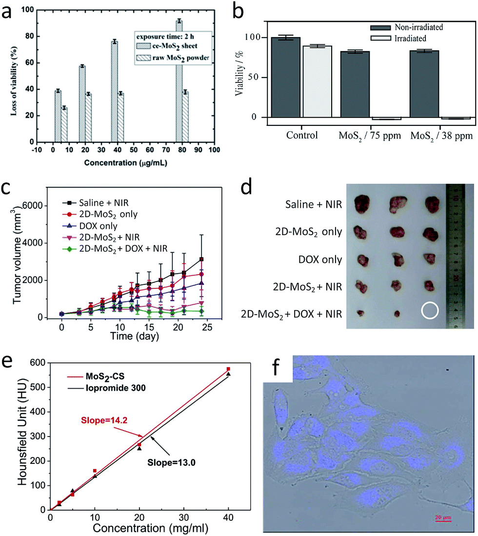 | ||
| Fig. 9 (a) The change of the viability of E. coli DH5α upon exposure to 2D MoS2 suspension upon varying concentration for 2 hours.202 Chemically exfoliated samples show higher antibacterial activity than raw ones. (b) The change of viability of HeLa cells with or without treatment with 2D MoS2 or NIR irradiation.203 Most of cells are dead when 2D MoS2 is injected with NIR irradiation, otherwise most of them are alive. (c) and (d): In vivo phototherapy of pancreatic tumour showing synergetic effect from combination of 2D MoS2 hyperthermia and doxocurbin chemotherapy, with the daily tumour growth curve (c) and the photographs of the tumour after 24 days of treatment (d).204 Here 2D MoS2 dose is 2.0 mg kg−1, and that of DOX is 0.95 mg kg−1, with NIR (808 nm laser) irradiation of 0.9 W cm−2 for 7 minutes. (e) Hounsfield units, the CT contrast value, of different concentrations of the contrasting reagents: MoS2 (red) and commercially used Iopromide 300 (black).204 (f) A combined image of the photoluminescence image (the purple coloured image) and the optical image (the background and the greyscale image) of HeLa cells, treated with of 1 μg mL−1 of MoS2.205 Reproduced with permission from: (a) ref. 202 © 2014 Royal Society of Chemistry; (b) ref. 203 © 2012 John Wiley and Sons; (c), (d) and (e): ref. 204 © 2014 American Chemical Society; (f) ref. 205 © 2014 Royal Society of Chemistry. | ||
Another application is photothermal therapy, which takes advantage of its good dispersibility and superior absorbance of near infrared (NIR).203 A 2D MoS2 dispersion shows 7.8 times higher absorbance than GO, and its extinction coefficients at 800 nm is 29.2 L g−1 cm−1, which is higher than gold nanorods. 2D MoS2 is biocompatible, as confirmed by complexation with α-chymotrypsin, where denaturation does not occur. A NIR and 2D MoS2 treatment of HeLa cells shows its superior in vitro photothermal therapy efficiency (Fig. 9b).203 In addition, incorporation of chitosan during exfoliation further enhances MoS2 biocompatibility and increases the photothermal conversion efficiency up to 24.37%.204 In vivo experiment on mice with pancreatic cancer (Panc-1 tumour) also confirms that chitosan-incorporated 2D MoS2 dispersion shows photothermal therapy upon NIR irradiation (Fig. 9c and d). A synergetic effect is created by further incorporation of doxocurbin (DOX), showing remarkable cancer-killing ability, as a result of the combination of hyperthermia and chemotherapy.
Visualisation of certain organs or cells is one of the most important functions for diagnosis and treatment. Based on the large atomic number of Mo, 2D MoS2 flakes can be used as CT image contrast agent.204 Its contrasting efficiency is comparable to commercially used Iopromide 300 contrast agent (Fig. 9e). It is also possible to directly visualise cells by PL from 2D MoS2, as confirmed by the uptake by HeLa cell.205 As shown in Fig. 9f, its fluorescence under UV light is observed within live HeLa cells, stating that 2D MoS2 does not harm the cells while retaining its properties.
7. Conclusions and outlooks
Atomic layers of MoS2 are one of the most attractive nanomaterials in recent years. Historically, this material has been a topic of research mainly for tribologists, intercalation chemists and petroleum chemists because of its aptness for such applications in the industry. Now, recent surging interests have expanded to scientists and engineers of all fields because of the attractive, useful properties of 2D MoS2 as an emerging nanomaterial. To this end, substantial research has been carried out in many fields of science and technology, which encompass not only historical research fields but also novel areas. These include nanoelectronics, which mainly concentrates on 2D MoS2 as a direct-gap semiconducting alternative of the metallic graphene. In other fields of research, numerous demonstrations such as FETs, molecular sensors, HER catalysts, or bioapplications have successfully demonstrated its bright potential for future applications. Reflecting upon these important aspects, it is clear that 2D MoS2 is now much closer to real applications than any other 2D nanomaterials.However, there are still many hurdles to overcome in order to bring its full potential into reality. For example, large-scale synthesis of single layers with single crystalline domain is still not achieved. Continuous films of 2D 1T-MoS2 have not been prepared yet. These high-quality large-scale films are the necessary starting point for applications such as large-scale device fabrication. In addition, catalyst efficiency is still too low to be applied in real industries, and thus further understanding and improvement are required. Heterostructure with other nanomaterials is still an unexplored area of research, which hold the potential of unprecedented, unique nature and applications.
2D MoS2 is one of the first 2D nanomaterials that have been studied other than graphene; several experimental techniques, strategic approaches, and demonstration of applications that are applied for graphene have been employed to 2D MoS2 as well. Such comparative studies suggest that these approaches are not only applicable to graphene but also applicable to other two-dimensional nanomaterials, providing a generalised route to study other unexplored 2D nanomaterials. In this sense, study on 2D MoS2 possesses great importance as a bridge that provides ways to expanding the scope of 2D nanomaterials.
Acknowledgements
I. Song, C. Park, and H. C. Choi appreciate the valuable comments by Ms. Lola Brown and Prof. Jiwoong Park at Cornell University. This work was supported by IBS-R014-G2 and NRF-2013K1A3A1A32035430. I. Song is grateful to Global Ph.D. Fellowship grant from NRF (NRF-2012H1A2A1016525).Notes and references
- J. G. Hooley, in Preparation and Crystal Growth of Materials with Layered Structures, ed. R. M. A. Lieth, D. Reidel Publishing Company, Dordrecht, 1977, pp. 1–33 Search PubMed.
- A. A. Balchin, in Crystallography and Crystal Chemistry of Materials with Layered Structures, ed. F. Lévy, D. Reidel Publishing Company, Dordrecht, 1976, pp. 1–50 Search PubMed.
- C. Y. Fong and M. Schluter, in Electrons and Phonons in Layered Crystal Structures, ed. T. J. Wieting and M. Schluter, D. Reidel Publishing Company, Dordrecht, 1979, pp. 145–320 Search PubMed.
- R. C. Fivaz and P. E. Schmid, in Optical and Electrical Properties, ed. P. A. Lee, D. Reidel Publishing Company, Dordrecht, 1976, pp. 343–384 Search PubMed.
- Preparation and Crystal Growth of Materials with Layered Structures, ed. R. M. A. Lieth, D. Reidel Publishing Company, Dordrecht, 1977 Search PubMed.
- M. M. Thackeray, J. O. Thomas and M. S. Whittingham, MRS Bull., 2000, 25, 39–46 CrossRef CAS.
- M. S. Dresselhaus, in Intercalation in Layered Materials, ed. M. S. Dresselhaus, Plenum Press, New York, 1986, pp. 1–30 Search PubMed.
- T. Bartels, W. Bock, J. Braun, C. Busch, W. Buss, W. Dresel, C. Freiler, M. Harperscheid, R.-P. Heckler, D. Hörner, F. Kubicki, G. Lingg, A. Losch, R. Luther, T. Mang, S. Noll and J. Omeis, in Ullmann's Encyclopedia of Industrial Chemistry, John Wiley and Sons-VCH Verlag GmbH & Co. KGaA, 2000 Search PubMed.
- K. S. Novoselov, A. K. Geim, S. V. Morozov, D. Jiang, Y. Zhang, S. V. Dubonos, I. V. Grigorieva and A. A. Firsov, Science, 2004, 306, 666–669 CrossRef CAS PubMed.
- K. S. Novoselov, D. Jiang, F. Schedin, T. J. Booth, V. V. Khotkevich, S. V. Morozov and A. K. Geim, Proc. Natl. Acad. Sci. U. S. A., 2005, 102, 10451–10453 CrossRef CAS PubMed.
- N. Coleman, M. Lotya, A. O'Neill, S. D. Bergin, P. J. King, U. Khan, K. Young, A. Gaucher, S. De, R. J. Smith, I. V. Shvets, S. K. Arora, G. Stanton, H. Y. Kim, K. Lee, G. T. Kim, G. S. Duesberg, T. Hallam, J. J. Boland, J. J. Wang, J. F. Donegan, J. C. Grunlan, G. Moriarty, A. Shmeliov, R. J. Nicholls, J. M. Perkins, E. M. Grieveson, K. Theuwissen, D. W. McComb, P. D. Nellist and V. Nicolosi, Science, 2011, 331, 568–571 CrossRef PubMed.
- A. K. Geim and K. S. Novoselov, Nat. Mater., 2007, 6, 183–191 CrossRef CAS PubMed.
- Q. H. Wang, K. Kalantar-Zadeh, A. Kis, J. N. Coleman and M. S. Strano, Nat. Nanotechnol., 2012, 7, 699–712 CrossRef CAS PubMed.
- M. Chhowalla, H. S. Shin, G. Eda, L.-J. Li, K. P. Loh and H. Zhang, Nat. Chem., 2013, 5, 263–275 CrossRef PubMed.
- G. A. Tsigdinos, in Aspects of Molybdenum and Related Chemistry, Springer-Verlag Berlin Heidelberg, New York, 1978, vol. 76, pp. 65–105 Search PubMed.
- R. F. Sebenik, A. R. Burkin, R. R. Dorfler, J. M. Laferty, G. Leichtfried, H. Meyer-Grünow, P. C. H. Mitchell, M. S. Vukasovich, D. A. Church, G. G. Van Riper, J. C. Gilliland and S. A. Thielke, Molybdenum and Molybdenum Compounds, Wiley-VCH Verlag GmbH & Co. KGaA, 2000 Search PubMed.
- E. R. Braithwaite and J. Haber, Molybdenum: an outline of its chemistry and uses, Elsevier, 1994 Search PubMed.
- W. Koehler, US Pat., 1 714 564, 1929.
- H. G. M. Fischer and R. P. Russell, US Pat., 2 322 622, 1943.
- R. P. Haering, J. A. R. Stiles and K. Brandt, US Pat., 4 224 390, 1980.
- Y. Feldman, E. Wasserman, D. J. Srolovitz and R. Tenne, Science, 1995, 267, 222–225 CrossRef CAS PubMed.
- Y. Feldman, G. L. Frey, M. Homyonfer, V. Lyakhovitskaya, L. Margulis, H. Cohen, G. Hodes, J. L. Hutchison and R. Tenne, J. Am. Chem. Soc., 1996, 118, 5362–5367 CrossRef CAS.
- G. L. Frey, R. Tenne, M. J. Matthews, M. S. Dresselhaus and G. Dresselhaus, J. Mater. Res., 1998, 13, 2412–2417 CrossRef CAS.
- R. Tenne, in The Chemistry of Nanostructured Materials, ed. P. Yang, World Sci. Publ., Singapore, 2003, pp. 147–182 Search PubMed.
- K. F. Mak, C. Lee, J. Hone, J. Shan and T. F. Heinz, Phys. Rev. Lett., 2010, 105, 136805 CrossRef.
- B. Radisavljevic, A. Radenovic, J. Brivio, V. Giacometti and A. Kis, Nat. Nanotechnol., 2011, 6, 147–150 CrossRef CAS PubMed.
- K. F. Mak, K. He, J. Shan and T. F. Heinz, Nat. Nanotechnol., 2012, 7, 494–498 CrossRef CAS PubMed.
- H. Zeng, J. Dai, W. Yao, D. Xiao and X. Cui, Nat. Nanotechnol., 2012, 7, 490–493 CrossRef CAS PubMed.
- T. Cao, G. Wang, W. Han, H. Ye, C. Zhu, J. Shi, Q. Niu, P. Tan, E. Wang, B. Liu and J. Feng, Nat. Commun., 2012, 3, 887 CrossRef PubMed.
- S. Wu, C. Huang, G. Aivazian, J. S. Ross, D. H. Cobden and X. Xu, ACS Nano, 2013, 7, 2768–2772 CrossRef CAS PubMed.
- T. F. Jaramillo, K. P. Jørgensen, J. Bonde, J. H. Nielsen, S. Horch and I. Chorkendorff, Science, 2007, 317, 100–102 CrossRef CAS PubMed.
- B. Hinnemann, P. G. Moses, J. Bonde, K. P. Jørgensen, J. H. Nielsen, S. Horch, I. Chorkendorff and J. K. Nørskov, J. Am. Chem. Soc., 2005, 127, 5308–5309 CrossRef CAS PubMed.
- H. Li, Z. Yin, Q. He, H. Li, X. Huang, G. Lu, D. W. H. Fam, A. I. Y. Tok, Q. Zhang and H. Zhang, Small, 2012, 8, 63–67 CrossRef CAS PubMed.
- F. E. Wickman and D. K. Smith, Am. Mineral., 1970, 55, 1843–1856 CAS.
- R. G. Dickinson and L. Pauling, J. Am. Chem. Soc., 1923, 45, 1466–1471 CrossRef CAS.
- F. Jellinek, G. Brauer and H. Muller, Nature, 1960, 185, 376–377 CrossRef CAS.
- F. Wypych and R. Schollhorn, J. Chem. Soc., Chem. Commun., 1992, 1386–1388 RSC.
- A. N. Enyashin, L. Yadgarov, L. Houben, I. Popov, M. Weidenbach, R. Tenne, M. Bar-Sadan and G. Seifert, J. Phys. Chem. C, 2011, 115, 24586–24591 CAS.
- F. Wypych, T. Weber and R. Prins, Chem. Mater., 1998, 10, 723–727 CrossRef CAS.
- R. V. Kasowski, Phys. Rev. Lett., 1973, 30, 1175–1178 CrossRef CAS.
- R. Fivaz and E. Mooser, Phys. Rev., 1967, 163, 743–755 CrossRef CAS.
- A. N. Enyashin and G. Seifert, Comput. Theor. Chem., 2012, 999, 13–20 CrossRef CAS PubMed.
- R. Huisman, R. de Jonge, C. Haas and F. Jellinek, J. Solid State Chem., 1971, 3, 56–66 CrossRef CAS.
- D. W. Bullett, J. Phys. C: Solid State Phys., 1978, 11, 4501–4514 CrossRef CAS.
- W. Jaegermann and H. Tributsch, Prog. Surf. Sci., 1988, 29, 1–167 CrossRef CAS.
- V. Alexiev, R. Prins and T. Weber, Phys. Chem. Chem. Phys., 2000, 2, 1815–1827 RSC.
- A. Clark and R. H. Williams, J. Phys. D: Appl. Phys., 1968, 1, 1222–1224 Search PubMed.
- R. Suzuki, M. Sakano, Y. J. Zhang, R. Akashi, D. Morikawa, a. Harasawa, K. Yaji, K. Kuroda, K. Miyamoto, T. Okuda, K. Ishizaka, R. Arita and Y. Iwasa, Nat. Nanotechnol., 2014, 9, 611–617 CrossRef CAS PubMed.
- T. Wieting and J. Verble, Phys. Rev. B: Condens. Matter Mater. Phys., 1971, 3, 4286–4292 CrossRef.
- J. L. Verble, T. J. Wietling and P. R. Reed, Solid State Commun., 1972, 11, 941–944 CrossRef CAS.
- W. Y. Liang, in Intercalation in Layered Materials, ed. M. S. Dresselhaus, Plenum Press, New York, 1986, pp. 31–73 Search PubMed.
- Z.-H. Chi, X.-M. Zhao, H. Zhang, A. F. Goncharov, S. S. Lobanov, T. Kagayama, M. Sakata and X.-J. Chen, Phys. Rev. Lett., 2014, 113, 036802 CrossRef.
- J. A. Woollam and R. B. Somoano, Phys. Rev. B: Condens. Matter Mater. Phys., 1976, 13, 3843–3853 CrossRef CAS.
- R. Somoano and A. Rembaum, Phys. Rev. Lett., 1971, 27, 402–404 CrossRef CAS.
- D. Liu, X. Chen, D. Li, F. Wang, X. Luo and B. Yang, J. Mol. Struct., 2010, 980, 66–71 CrossRef CAS PubMed.
- D. Godfrey and E. C. Nelson, Oxidation Characteristic of Molybdenum Disulfide and Effect of Such Oxidation on Its Role as a Solid-film Lubricant: N.A.C.A. Technical Note No. 1882, National Advisory Committee for Aeronautics, Washington, D. C., 1949 Search PubMed.
- J. A. Wilson and A. D. Yoffe, Adv. Phys., 1969, 18, 193–335 CrossRef CAS.
- Q. Li, E. C. Walter, W. E. van der Veer, B. J. Murray, J. T. Newberg, E. W. Bohannan, J. A. Switzer, J. C. Hemminger and R. M. Penner, J. Phys. Chem. B, 2005, 109, 3169–3182 CrossRef CAS PubMed.
- J. W. Frondel and F. E. Wickman, Am. Mineral., 1970, 55, 1857–1875 CAS.
- J. R. Stubbles and F. D. Richardson, Trans. Faraday Soc., 1960, 56, 1460–1466 RSC.
- T. Prasad, J. Inorg. Nucl. Chem., 1973, 35, 1895–1904 CrossRef CAS.
- R. E. Bell and R. E. Herfert, J. Am. Chem. Soc., 1957, 79, 3351–3354 CrossRef CAS.
- M. S. Silverman, Inorg. Chem., 1967, 6, 1063–1064 CrossRef CAS.
- J. C. Wildervanck and F. Jellinek, Z. Anorg. Allg. Chem., 1964, 328, 309–318 CrossRef CAS.
- W. O. Winer, Wear, 1967, 10, 422–452 CrossRef CAS.
- R. Holinski and J. Gänsheimer, Wear, 1972, 19, 329–342 CrossRef CAS.
- P. D. Fleischauer, J. R. Lince, P. A. Bertrand and R. Bauer, Langmuir, 1989, 5, 1009–1015 CrossRef CAS.
- A. R. Lansdown, Molybdenum Disulphide Lubrication, Elsevier Science, Amsterdam, 1999 Search PubMed.
- J. M. Martin, H. Pascal, C. Donnet, T. Le Mogne, J. L. Loubet and T. Epicier, Surf. Coat. Technol., 1994, 68–69, 427–432 CrossRef.
- D. F. Moore, Principles and Applications of Tribology, Pergamon Press Inc., New York, 1975 Search PubMed.
- A. Savan, E. Pflüger, P. Voumard, A. Schröer and M. Simmonds, Lubr. Sci., 2000, 12, 185–203 CrossRef CAS.
- R. H. Savage, J. Appl. Phys., 1948, 19, 1–10 CrossRef CAS PubMed.
- P. J. Bryant, P. L. Gutshall and L. H. Taylor, Wear, 1964, 7, 118–126 CrossRef.
- A. J. Haltner, Wear, 1964, 7, 102–117 CrossRef.
- A. J. Haltner and C. S. Oliver, Ind. Eng. Chem. Fundam., 1966, 5, 348–355 CAS.
- L. W. Vernon and J. T. Richardson, US Pat., 3 000 816, 1961.
- H. Topsøe, B. S. Clausen and F. E. Massoth, in Catalysis-Science and Technology, ed. J. R. Anderson and M. Boudart, Springer Berlin Heidelberg, Berlin, Heidelberg, 1996, pp. 1–269 Search PubMed.
- L. S. Byskov, J. K. Nørskov, B. S. Clausen and H. Topsøe, J. Catal., 1999, 187, 109–122 CrossRef CAS.
- F. Wypych, K. Sollmann and R. Schöllhorn, Mater. Res. Bull., 1992, 27, 545–553 CrossRef CAS.
- Y.-C. Lin, D. O. Dumcenco, Y.-S. Huang and K. Suenaga, Nat. Nanotechnol., 2014, 9, 391–396 CrossRef CAS PubMed.
- P. J. Mulhern, Can. J. Phys., 1989, 67, 1049–1052 CrossRef CAS PubMed.
- D. Yang, S. Sandoval, W. Divigalpitiya, J. Irwin and R. Frindt, Phys. Rev. B: Condens. Matter Mater. Phys., 1991, 43, 12053–12056 CrossRef CAS.
- K. E. Dungey, M. D. Curtis and J. E. Penner-Hahn, Chem. Mater., 1998, 10, 2152–2161 CrossRef CAS.
- J. Heising and M. G. Kanatzidis, J. Am. Chem. Soc., 1999, 121, 11720–11732 CrossRef CAS.
- E. Benavente, M. A. S. Ana, F. Mendizábal and G. González, Coord. Chem. Rev., 2002, 224, 87–109 CrossRef CAS.
- C. Julien, S. I. Saikh and G. A. Nazri, Mater. Sci. Eng. B, 1992, 15, 73–77 CrossRef.
- M. B. Dines, Science, 1975, 188, 1210–1211 CAS.
- R. Bissessur, J. Heising, W. Hirpo and M. Kanatzidis, Chem. Mater., 1996, 8, 318–320 CrossRef CAS.
- L. Wang, J. Schindler, J. A. Thomas, C. R. Kannewurf and M. G. Kanatzidis, Chem. Mater., 1995, 7, 1753–1755 CrossRef CAS.
- T. Stephenson, Z. Li, B. Olsen and D. Mitlin, Energy Environ. Sci., 2014, 7, 209–231 CAS.
- J. O. Besenhard, J. Yang and M. Winter, J. Power Sources, 1997, 68, 87–90 CrossRef CAS.
- H. Hwang, H. Kim and J. Cho, Nano Lett., 2011, 11, 4826–4830 CrossRef CAS PubMed.
- Y. Y. Wang, R. X. Gao, Z. H. Ni, H. He, S. P. Guo, H. P. Yang, C. X. Cong and T. Yu, Nanotechnology, 2012, 23, 495713 CrossRef PubMed.
- M. M. Benameur, B. Radisavljevic, J. S. Héron, S. Sahoo, H. Berger and A. Kis, Nanotechnology, 2011, 22, 125706 CrossRef CAS PubMed.
- P. Blake, E. W. Hill, A. H. Castro Neto, K. S. Novoselov, D. Jiang, R. Yang, T. J. Booth and A. K. Geim, Appl. Phys. Lett., 2007, 91, 063124 CrossRef PubMed.
- H. Li, G. Lu, Z. Yin, Q. He, H. Li, Q. Zhang and H. Zhang, Small, 2012, 8, 682–686 CrossRef CAS PubMed.
- A. Castellanos-Gomez, M. Barkelid, A. M. Goossens, V. E. Calado, H. S. J. van der Zant and G. A. Steele, Nano Lett., 2012, 12, 3187–3192 CrossRef CAS PubMed.
- R. Ruoff, Nat. Nanotechnol., 2008, 3, 10–11 CrossRef CAS PubMed.
- P. Joensen, R. F. Frindt and S. R. Morrison, Mater. Res. Bull., 1986, 21, 457–461 CrossRef CAS.
- H. S. S. Ramakrishna Matte, A. Gomathi, A. K. Manna, D. J. Late, R. Datta, S. K. Pati and C. N. R. Rao, Angew. Chem., Int. Ed., 2010, 49, 4059–4062 CrossRef PubMed.
- Z. Zeng, Z. Yin, X. Huang, H. Li, Q. He, G. Lu, F. Boey and H. Zhang, Angew. Chem., Int. Ed., 2011, 50, 11093–11097 CrossRef CAS PubMed.
- G. Eda, T. Fujita, H. Yamaguchi, D. Voiry, M. Chen and M. Chhowalla, ACS Nano, 2012, 6, 7311–7317 CrossRef CAS PubMed.
- M. A. Lukowski, A. S. Daniel, F. Meng, A. Forticaux, L. Li and S. Jin, J. Am. Chem. Soc., 2013, 135, 10274–10277 CrossRef CAS PubMed.
- D. Voiry, M. Salehi, R. Silva, T. Fujita, M. Chen, T. Asefa, V. B. Shenoy, G. Eda and M. Chhowalla, Nano Lett., 2013, 13, 6222–6227 CrossRef CAS PubMed.
- R. J. Smith, P. J. King, M. Lotya, C. Wirtz, U. Khan, S. De, A. O'Neill, G. S. Duesberg, J. C. Grunlan, G. Moriarty, J. Chen, J. Wang, A. I. Minett, V. Nicolosi and J. N. Coleman, Adv. Mater., 2011, 23, 3944–3948 CrossRef CAS PubMed.
- P. Afanasiev, G.-F. Xia, G. Berhault, B. Jouguet and M. Lacroix, Chem. Mater., 1999, 11, 3216–3219 CrossRef CAS.
- K.-G. Zhou, N.-N. Mao, H.-X. Wang, Y. Peng and H.-L. Zhang, Angew. Chem., Int. Ed., 2011, 50, 10839–10842 CrossRef CAS PubMed.
- G. Cunningham, M. Lotya, C. S. Cucinotta, S. Sanvito, S. D. Bergin, R. Menzel, M. S. P. Shaffer and J. N. Coleman, ACS Nano, 2012, 6, 3468–3480 CrossRef CAS PubMed.
- N. Liu, P. Kim, J. H. Kim, J. H. Ye, S. Kim and C. J. Lee, ACS Nano, 2014, 8, 6902–6910 CrossRef CAS PubMed.
- K. Lee, H.-Y. Kim, M. Lotya, J. N. Coleman, G.-T. Kim and G. S. Duesberg, Adv. Mater., 2011, 23, 4178–4182 CrossRef CAS PubMed.
- G. Eda, H. Yamaguchi, D. Voiry, T. Fujita, M. Chen and M. Chhowalla, Nano Lett., 2011, 11, 5111–5116 CrossRef CAS PubMed.
- A. O'Neill, U. Khan and J. N. Coleman, Chem. Mater., 2012, 24, 2414–2421 CrossRef.
- J. Brivio, D. T. L. Alexander and A. Kis, Nano Lett., 2011, 11, 5148–5153 CrossRef CAS PubMed.
- S. Helveg, J. Lauritsen, E. Laegsgaard, I. Stensgaard, J. Nørskov, B. Clausen, H. Tøpsoe and F. Besenbacher, Phys. Rev. Lett., 2000, 84, 951–954 CrossRef CAS.
- D. Kim, D. Sun, W. Lu, Z. Cheng, Y. Zhu, D. Le, T. S. Rahman and L. Bartels, Langmuir, 2011, 27, 11650–11653 CrossRef CAS PubMed.
- Y. Zhan, Z. Liu, S. Najmaei, P. M. Ajayan and J. Lou, Small, 2012, 8, 966–971 CrossRef CAS PubMed.
- Y. Lee, J. Lee, H. Bark, I.-K. Oh, G. H. Ryu, Z. Lee, H. Kim, J. H. Cho, J.-H. Ahn and C. Lee, Nanoscale, 2014, 6, 2821–2826 RSC.
- D. Kong, H. Wang, J. J. Cha, M. Pasta, K. J. Koski, J. Yao and Y. Cui, Nano Lett., 2013, 13, 1341–1347 CrossRef CAS PubMed.
- M. Schleberger, D. Fujita, C. Scharfschwerdt and S. Tougaard, Surf. Sci., 1995, 331–333, 942–947 CrossRef CAS.
- Y. Shi, W. Zhou, A.-Y. Lu, W. Fang, Y.-H. Lee, A. L. Hsu, S. M. Kim, K. K. Kim, H. Y. Yang, L.-J. Li, J.-C. Idrobo and J. Kong, Nano Lett., 2012, 12, 2784–2791 CrossRef CAS PubMed.
- K.-K. Liu, W. Zhang, Y.-H. Lee, Y.-C. Lin, M.-T. Chang, C.-Y. Su, C.-S. Chang, H. Li, Y. Shi, H. Zhang, C.-S. Lai and L.-J. Li, Nano Lett., 2012, 12, 1538–1544 CrossRef CAS PubMed.
- Y.-H. Lee, X.-Q. Zhang, W. Zhang, M.-T. Chang, C.-T. Lin, K.-D. Chang, Y.-C. Yu, J. T.-W. Wang, C.-S. Chang, L.-J. Li and T.-W. Lin, Adv. Mater., 2012, 24, 2320–2325 CrossRef CAS PubMed.
- Y.-C. Lin, W. Zhang, J.-K. Huang, K.-K. Liu, Y.-H. Lee, C.-T. Liang, C.-W. Chu and L.-J. Li, Nanoscale, 2012, 4, 6637–6641 RSC.
- Y. Yu, C. Li, Y. Liu, L. Su, Y. Zhang and L. Cao, Sci. Rep., 2013, 3, 1866 Search PubMed.
- X. Wang, H. Feng, Y. Wu and L. Jiao, J. Am. Chem. Soc., 2013, 135, 5304–5307 CrossRef CAS PubMed.
- Y.-H. Lee, L. Yu, H. Wang, W. Fang, X. Ling, Y. Shi, C.-T. Lin, J.-K. Huang, M.-T. Chang, C.-S. Chang, M. Dresselhaus, T. Palacios, L.-J. Li and J. Kong, Nano Lett., 2013, 13, 1852–1857 CAS.
- Q. Ji, Y. Zhang, T. Gao, Y. Zhang, D. Ma, M. Liu, Y. Chen, X. Qiao, P.-H. Tan, M. Kan, J. Feng, Q. Sun and Z. Liu, Nano Lett., 2013, 13, 3870–3877 CrossRef CAS PubMed.
- I. Song, C. Park, M. Hong, J. Baik, H.-J. Shin and H. C. Choi, Angew. Chem., Int. Ed., 2014, 53, 1266–1269 CrossRef CAS PubMed.
- A. M. van der Zande, P. Y. Huang, D. A. Chenet, T. C. Berkelbach, Y. You, G.-H. Lee, T. F. Heinz, D. R. Reichman, D. A. Muller and J. C. Hone, Nat. Mater., 2013, 12, 554–561 CrossRef CAS PubMed.
- Y. Liu, R. Ghosh, D. Wu, A. Ismach, R. Ruoff and K. Lai, Nano Lett., 2014, 14, 4682–4686 CrossRef CAS PubMed.
- P. Y. Huang, C. S. Ruiz-Vargas, A. M. van der Zande, W. S. Whitney, M. P. Levendorf, J. W. Kevek, S. Garg, J. S. Alden, C. J. Hustedt, Y. Zhu, J. Park, P. L. McEuen and D. A. Muller, Nature, 2011, 469, 389–392 CrossRef CAS PubMed.
- S. Najmaei, Z. Liu, W. Zhou, X. Zou, G. Shi, S. Lei, B. I. Yakobson, J.-C. Idrobo, P. M. Ajayan and J. Lou, Nat. Mater., 2013, 12, 754–759 CrossRef CAS PubMed.
- W. Zhou, X. Zou, S. Najmaei, Z. Liu, Y. Shi, J. Kong, J. Lou, P. M. Ajayan, B. I. Yakobson and J.-C. Idrobo, Nano Lett., 2013, 13, 2615–2622 CrossRef CAS PubMed.
- S. Najmaei, M. Amani, M. L. Chin, Z. Liu, A. G. Birdwell, T. P. O'Regan, P. M. Ajayan, M. Dubey and J. Lou, ACS Nano, 2014, 8, 7930–7937 CrossRef CAS PubMed.
- A. Splendiani, L. Sun, Y. Zhang, T. Li, J. Kim, C.-Y. Chim, G. Galli and F. Wang, Nano Lett., 2010, 10, 1271–1275 CrossRef CAS PubMed.
- X. Li, X. Wang, L. Zhang, S. Lee and H. Dai, Science, 2008, 319, 1229–1232 CrossRef CAS PubMed.
- T. Böker, R. Severin, A. Müller, C. Janowitz, R. Manzke, D. Voß, P. Krüger, A. Mazur and J. Pollmann, Phys. Rev. B: Condens. Matter Mater. Phys., 2001, 64, 235305 CrossRef.
- S. Lebègue and O. Eriksson, Phys. Rev. B: Condens. Matter Mater. Phys., 2009, 79, 115409 CrossRef.
- C. R. Zhu, G. Wang, B. L. Liu, X. Marie, X. F. Qiao, X. Zhang, X. X. Wu, H. Fan, P. H. Tan, T. Amand and B. Urbaszek, Phys. Rev. B: Condens. Matter Mater. Phys., 2013, 88, 121301 CrossRef.
- H. J. Conley, B. Wang, J. I. Ziegler, R. F. Haglund, S. T. Pantelides and K. I. Bolotin, Nano Lett., 2013, 13, 3626–3630 CrossRef CAS PubMed.
- A. Castellanos-Gomez, R. Roldán, E. Cappelluti, M. Buscema, F. Guinea, H. S. J. van der Zant and G. A. Steele, Nano Lett., 2013, 13, 5361–5366 CrossRef CAS PubMed.
- S. N. Shirodkar and U. V. Waghmare, Phys. Rev. Lett., 2014, 112, 157601 CrossRef.
- D. Jena and A. Konar, Phys. Rev. Lett., 2007, 98, 136805 CrossRef.
- M. S. Fuhrer and J. Hone, Nat. Nanotechnol., 2013, 8, 146–147 CrossRef CAS PubMed.
- B. Radisavljevic and A. Kis, Nat. Nanotechnol., 2013, 8, 147–148 CrossRef CAS PubMed.
- K. Kaasbjerg, K. S. Thygesen and K. W. Jacobsen, Phys. Rev. B: Condens. Matter Mater. Phys., 2012, 85, 115317 CrossRef.
- S. Kim, A. Konar, W.-S. Hwang, J. H. Lee, J. Lee, J. Yang, C. Jung, H. Kim, J.-B. Yoo, J.-Y. Choi, Y. W. Jin, S. Y. Lee, D. Jena, W. Choi and K. Kim, Nat. Commun., 2012, 3, 1011 CrossRef PubMed.
- F. L. Deepak, H. Cohen, S. Cohen, Y. Feldman, R. Popovitz-Biro, D. Azulay, O. Millo and R. Tenne, J. Am. Chem. Soc., 2007, 129, 12549–12562 CrossRef CAS PubMed.
- V. V. Ivanovskaya, T. Heine, S. Gemming and G. Seifert, Phys. Status Solidi B, 2006, 243, 1757–1764 CrossRef CAS.
- M. R. Laskar, D. N. Nath, L. Ma, E. W. Lee, C. H. Lee, T. Kent, Z. Yang, R. Mishra, M. A. Roldan, J.-C. Idrobo, S. T. Pantelides, S. J. Pennycook, R. C. Myers, Y. Wu and S. Rajan, Appl. Phys. Lett., 2014, 104, 092104 CrossRef PubMed.
- Y.-C. Lin, D. O. Dumcenco, H.-P. Komsa, Y. Niimi, A. V. Krasheninnikov, Y.-S. Huang and K. Suenaga, Adv. Mater., 2014, 26, 2857–2861 CrossRef CAS PubMed.
- L. Yadgarov, R. Rosentsveig, G. Leitus, A. Albu-Yaron, A. Moshkovich, V. Perfilyev, R. Vasic, A. I. Frenkel, A. N. Enyashin, G. Seifert, L. Rapoport and R. Tenne, Angew. Chem., Int. Ed., 2011, 2, 1–5 Search PubMed.
- K. Dolui, I. Rungger, C. Das Pemmaraju and S. Sanvito, Phys. Rev. B: Condens. Matter Mater. Phys., 2013, 88, 075420 CrossRef.
- H. Fang, M. Tosun, G. Seol, T. C. Chang, K. Takei, J. Guo and A. Javey, Nano Lett., 2013, 13, 1991–1995 CrossRef CAS PubMed.
- K. Dolui, I. Rungger and S. Sanvito, Phys. Rev. B: Condens. Matter Mater. Phys., 2013, 87, 165402 CrossRef.
- B. Radisavljevic and A. Kis, Nat. Mater., 2013, 12, 815–820 CrossRef CAS PubMed.
- J. T. Ye, Y. J. Zhang, R. Akashi, M. S. Bahramy, R. Arita and Y. Iwasa, Science, 2012, 338, 1193–1196 CrossRef CAS PubMed.
- K. Taniguchi, A. Matsumoto, H. Shimotani and H. Takagi, Appl. Phys. Lett., 2012, 101, 042603 CrossRef PubMed.
- I. Popov, G. Seifert and D. Tománek, Phys. Rev. Lett., 2012, 108, 156802 CrossRef.
- S. Das, H.-Y. Chen, A. V. Penumatcha and J. Appenzeller, Nano Lett., 2013, 13, 100–105 CrossRef CAS PubMed.
- J. Kang, W. Liu and K. Banerjee, Appl. Phys. Lett., 2014, 104, 093106 CrossRef PubMed.
- Y. Yoon, K. Ganapathi and S. Salahuddin, Nano Lett., 2011, 11, 3768–3773 CrossRef CAS PubMed.
- H.-Y. Chang, S. Yang, J. Lee, L. Tao, W.-S. Hwang, D. Jena, N. Lu and D. Akinwande, ACS Nano, 2013, 7, 5446–5452 CrossRef CAS PubMed.
- Y. Zhang, J. Ye, Y. Matsuhashi and Y. Iwasa, Nano Lett., 2012, 12, 1136–1140 CrossRef CAS PubMed.
- W. Bao, X. Cai, D. Kim, K. Sridhara and M. S. Fuhrer, Appl. Phys. Lett., 2013, 102, 042104 CrossRef PubMed.
- Y. J. Zhang, J. T. Ye, Y. Yomogida, T. Takenobu and Y. Iwasa, Nano Lett., 2013, 13, 3023–3028 CrossRef CAS PubMed.
- B. Radisavljevic, M. B. Whitwick and A. Kis, ACS Nano, 2011, 5, 9934–9938 CrossRef CAS PubMed.
- T. Cheiwchanchamnangij and W. R. L. Lambrecht, Phys. Rev. B: Condens. Matter Mater. Phys., 2012, 85, 205302 CrossRef.
- Y. Wang, J. Z. Ou, S. Balendhran, A. F. Chrimes, M. Mortazavi, D. D. Yao, M. R. Field, K. Latham, V. Bansal, J. R. Friend, S. Zhuiykov, N. V. Medhekar, M. S. Strano and K. Kalantar-zadeh, ACS Nano, 2013, 7, 10083–10093 CrossRef CAS PubMed.
- K. F. Mak, K. L. McGill, J. Park and P. L. McEuen, Science, 2014, 344, 1489–1492 CrossRef CAS PubMed.
- K. F. Mak, K. He, C. Lee, G. H. Lee, J. Hone, T. F. Heinz and J. Shan, Nat. Mater., 2013, 12, 207–211 CrossRef CAS PubMed.
- S. Mouri, Y. Miyauchi and K. Matsuda, Nano Lett., 2013, 13, 5944–5948 CrossRef CAS PubMed.
- C. Lee, H. Yan, L. E. Brus, T. F. Heinz, J. Hone and S. Ryu, ACS Nano, 2010, 4, 2695–2700 CrossRef CAS PubMed.
- A. Molina-Sánchez and L. Wirtz, Phys. Rev. B: Condens. Matter Mater. Phys., 2011, 84, 155413 CrossRef.
- H. Li, Q. Zhang, C. C. R. Yap, B. K. Tay, T. H. T. Edwin, A. Olivier and D. Baillargeat, Adv. Funct. Mater., 2012, 22, 1385–1390 CrossRef CAS.
- L. Sun, J. Yan, D. Zhan, L. Liu, H. Hu, H. Li, B. K. Tay, J.-L. Kuo, C.-C. Huang, D. W. Hewak, P. S. Lee and Z. X. Shen, Phys. Rev. Lett., 2013, 111, 126801 CrossRef.
- M. Buscema, M. Barkelid, V. Zwiller, H. S. J. van der Zant, G. A. Steele and A. Castellanos-Gomez, Nano Lett., 2013, 13, 358–363 CrossRef CAS PubMed.
- Z. Yin, H. Li, H. Li, L. Jiang, Y. Shi, Y. Sun, G. Lu, Q. Zhang, X. Chen and H. Zhang, ACS Nano, 2012, 6, 74–80 CrossRef CAS PubMed.
- O. Lopez-Sanchez, D. Lembke, M. Kayci, A. Radenovic and A. Kis, Nat. Nanotechnol., 2013, 8, 497–501 CrossRef CAS PubMed.
- W. Zhang, J.-K. Huang, C.-H. Chen, Y.-H. Chang, Y.-J. Cheng and L.-J. Li, Adv. Mater., 2013, 25, 3456–3461 CrossRef CAS PubMed.
- H. S. Lee, S.-W. Min, Y.-G. Chang, M. K. Park, T. Nam, H. Kim, J. H. Kim, S. Ryu and S. Im, Nano Lett., 2012, 12, 3695–3700 CrossRef CAS PubMed.
- M.-L. Tsai, S.-H. Su, J.-K. Chang, D.-S. Tsai, C.-H. Chen, C.-I. Wu, L.-J. Li, L.-J. Chen and J.-H. He, ACS Nano, 2014, 8, 8317–8322 CrossRef CAS PubMed.
- X. Gu, W. Cui, H. Li, Z. Wu, Z. Zeng, S.-T. Lee, H. Zhang and B. Sun, Adv. Energy Mater., 2013, 3, 1262–1268 CrossRef CAS.
- R. S. Sundaram, M. Engel, A. Lombardo, R. Krupke, A. C. Ferrari, P. Avouris and M. Steiner, Nano Lett., 2013, 13, 1416–1421 CAS.
- S. Bertolazzi, J. Brivio and A. Kis, ACS Nano, 2011, 5, 9703–9709 CrossRef CAS PubMed.
- A. Castellanos-Gomez, M. Poot, G. a. Steele, H. S. J. van der Zant, N. Agraït and G. Rubio-Bollinger, Adv. Mater., 2012, 24, 772–775 CrossRef CAS PubMed.
- D. Sarkar, W. Liu, X. Xie, A. C. Anselmo, S. Mitragotri and K. Banerjee, ACS Nano, 2014, 8, 3992–4003 CrossRef CAS PubMed.
- D. J. Late, Y. Huang, B. Liu, J. Acharya, S. N. Shirodkar, J. Luo, A. Yan, D. Charles, U. V Waghmare, V. P. Dravid and C. N. R. Rao, ACS Nano, 2013, 7, 4879–4891 CrossRef CAS PubMed.
- Q. Yue, Z. Shao, S. Chang and J. Li, Nanoscale Res. Lett., 2013, 8, 425 CrossRef PubMed.
- C. Zhu, Z. Zeng, H. Li, F. Li, C. Fan and H. Zhang, J. Am. Chem. Soc., 2013, 135, 5998–6001 CrossRef CAS PubMed.
- A. Tuxen, J. Kibsgaard, H. Gøbel, E. Lægsgaard, H. Topsøe, J. V. Lauritsen and F. Besenbacher, ACS Nano, 2010, 4, 4677–4682 CrossRef CAS PubMed.
- R. R. Chianelli, M. H. Siadati, M. P. De la Rosa, G. Berhault, J. P. Wilcoxon, R. Bearden and B. L. Abrams, Catal. Rev., 2006, 48, 1–41 CAS.
- A. Sobczynski, J. Catal., 1991, 131, 156–166 CrossRef CAS.
- Y. Li, H. Wang, L. Xie, Y. Liang, G. Hong and H. Dai, J. Am. Chem. Soc., 2011, 133, 7296–7299 CrossRef CAS PubMed.
- X. Huang, Z. Zeng, S. Bao, M. Wang, X. Qi, Z. Fan and H. Zhang, Nat. Commun., 2013, 4, 1444 CrossRef PubMed.
- U. Maitra, U. Gupta, M. De, R. Datta, A. Govindaraj and C. N. R. Rao, Angew. Chem., Int. Ed., 2013, 52, 13057–13061 CrossRef CAS PubMed.
- H. Wang, Z. Lu, S. Xu, D. Kong, J. J. Cha, G. Zheng, P.-C. Hsu, K. Yan, D. Bradshaw, F. B. Prinz and Y. Cui, Proc. Natl. Acad. Sci. U. S. A., 2013, 110, 19701–19706 CrossRef CAS PubMed.
- X. Zong, H. Yan, G. Wu, G. Ma, F. Wen, L. Wang and C. Li, J. Am. Chem. Soc., 2008, 130, 7176–7177 CrossRef CAS PubMed.
- Y. Li, Y.-L. Li, C. M. Araujo, W. Luo and R. Ahuja, Catal. Sci. Technol., 2013, 3, 2214–2220 CAS.
- Z. Yin, B. Chen, M. Bosman, X. Cao, J. Chen, B. Zheng and H. Zhang, Small, 2014, 10, 3537–3543 CrossRef CAS PubMed.
- M. D. J. Quinn, N. H. Ho and S. M. Notley, ACS Appl. Mater. Interfaces, 2013, 5, 12751–12756 CAS.
- X. Yang, J. Li, T. Liang, C. Ma, Y. Zhang, H. Chen, N. Hanagata, H. Su and M. Xu, Nanoscale, 2014, 6, 10126–10133 RSC.
- S. S. Chou, B. Kaehr, J. Kim, B. M. Foley, M. De, P. E. Hopkins, J. Huang, C. J. Brinker and V. P. Dravid, Angew. Chem., Int. Ed., 2013, 52, 4160–4164 CrossRef CAS PubMed.
- W. Yin, L. Yan, J. Yu, G. Tian, L. Zhou, X. Zheng, X. Zhang, Y. Yong, J. Li, Z. Gu and Y. Zhao, ACS Nano, 2014, 8, 6922–6933 CrossRef CAS PubMed.
- R. Anbazhagan, H.-J. Wang, H.-C. Tsai and R.-J. Jeng, RSC Adv., 2014, 4, 42936–42941 RSC.
| This journal is © The Royal Society of Chemistry 2015 |