One-minute deposition of micrometre-thick porous Si anodes for lithium ion batteries

Jungho Leeab and Suguru Noda*b
aDepartment of Chemical System Engineering, The University of Tokyo, 7-3-1 Hongo, Bunkyo-ku, Tokyo 113-8656, Japan
bDepartment of Applied Chemistry, Waseda University, 3-4-1 Okubo, Shinjuku-ku, Tokyo 169-8555, Japan. E-mail: noda@waseda.jp; Fax: +81-3-5286-2769; Tel: +81-3-5286-2769

Received 2nd October 2014 , Accepted 28th November 2014

First published on 2nd December 2014


Abstract

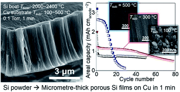
We report the rapid vapour deposition of 3–14 μm-thick porous Si anodes on Cu current collectors in 10–60 s. Such rapid deposition was achieved by heating the Si source to over 2000 °C, well above the melting point of Si, while the porous structure was realized in the deposited Si films by keeping the Cu collector at a much lower temperature of 100–500 °C. The adhesion between the Cu collectors and Si films was enhanced by forming a CuSix intermixed layer by post-deposition annealing as well as surface treatment of the Cu collectors. Half-cell measurements showed that the porous Si anodes without post-annealing degraded in a few cycles. A markedly improved cycle performance (1000 mA h gSi−1 and 0.66 mA h cmanode−2 at the anode for the 50th cycle) was achieved for post-annealed 3.5 μm-thick porous Si films. Rapid vapor deposition of micrometre-thick porous Si films using inexpensive, safe Si powder is a practical route to fabricate high-capacity anodes for lithium ion batteries.


Introduction

Advanced energy storage technology has recently been attracting much attention because of the increasing demand for energy storage systems and electric vehicles. To date, rechargeable lithium ion batteries (LIBs) have been successfully used with focus on portable electronic devices, hybrid and electric vehicles, and renewable energy storage.1–4 For high-capacity technology, LIBs with higher energy and power densities are required.5,6

The current choice of anode material for LIBs is usually graphite because of its long cycle life, abundance and relatively low cost.7 However, graphite anodes possess the disadvantages of low capacity (375 mA h gC−1) and safety issues related to Li deposition.8,9 Thus, there has been a growing interest in developing alternative anode materials with low cost, good safety, high energy density and long cycle life. Si is an attractive alloy-type anode material with a theoretical specific capacity (4200 mA h gSi−1) that is ten times larger than that of conventional graphite based on the stoichiometry of the alloy Li22Si5.10–12 However, this high specific capacity is realized by inserting a large amount of Li+ into the active material, which is accompanied with a four-fold volumetric expansion. Si electrodes are not able to withstand the heavy strain of such volumetric expansion and break down, resulting in pulverization and delamination of the whole structure.13–15 Further capacity losses are caused by solid electrolyte interphase (SEI) formation, while delamination results in loss of electrical contact with the current collector.

To overcome pulverization of electrodes during expansion and shrinkage, many groups, starting with the study by Huggins and coworkers,10 have developed various approaches to control electrode structures, initially thin films,16,17 microparticles,18 nanowires,19–23 nanoparticles,24,25 pillar formation,26 NiSix–Si core–shell nanowires,27 and other structures.28,29 Full cells comprising of C–Si core–shell nanowires30 have been reported. High capacities were reported for such structures; however, sometimes the weight of heavy current collectors was neglected for very thin active layers.

In this paper, we rapidly deposit 3–14 μm-thick porous Si films in 1 min or less by a physical vapour deposition method called rapid vapour deposition (RVD). Such a high deposition rate is achieved by heating the source Si to 2000–2400 °C, well above its melting point of 1414 °C. Control over the amorphous/crystalline structure, film porosity, surface roughness, and Si/Cu interface is realized by maintaining the temperature of the Cu substrate at 100–600 °C during and after deposition. In particular, control over the roughness of the growing Si films caused by the shadowing effect,31,32 is important to tailor the film microstructure. The electrochemical behaviour of the Si films was investigated by a half-cell test using Li as the counter electrode and discussed in relation to their microstructure.

Experimental

Si film fabrication

Circular Cu plates (15 mm in diameter, 0.5 mm in thickness) instead of thin Cu foils were used as substrates for porous Si films to make the handling (adjusting the size to fit the coin cells) easier. Before Si deposition, the Cu plates were sonicated in isopropanol for 10 min and then exposed to UV-O3 for 3 min to remove organic contaminants on their surface. Then, the Cu plates were annealed under hydrogen (5 vol% H2/Ar, 1 atm) at 800 °C for 10 min to reduce the oxide layer on the Cu surface. Finally, Si was deposited on the Cu substrates by RVD.

Fig. 1a shows a schematic diagram of the RVD system. The Si source for RVD was prepared by first immersing a Si wafer (CZ p-type, resistivity of 10–20 Ω cm) in 5 wt% hydrogen fluoride (HF) solution for 1 min, and then rinsing it with purified water for 1 min. The wafer was ground into Si powder using mortar and pestle and then loaded into a carbon boat. The Si source was heated by resistive heating of the carbon boat under 0.1 Torr Ar to 2000–2400 °C (boat temperature, Tboat) to increase its vapor pressure and thus the deposition rate. A Cu substrate was positioned in the chamber and kept at 100–500 °C (substrate temperature, Tsub) during RVD to suppress the surface diffusion of Si, which induces rough and porous structure in the deposited Si films.30,31 To maintain the Cu substrate at constant temperature under the strong thermal radiation from the Si source, we designed a substrate holder made of a block of Cu with a large heat capacity that contained an embedded ceramic heater and N2-gas cooling line. After removing the sample from the RVD system, some of the samples were further annealed under 4 vol% H2/Ar at ambient pressure at 200–600 °C (annealing temperature, Tan) for 10 min to form a CuSix intermixed layer to improve the adhesion between the Cu substrate and Si film.


image file: c4ra11681j-f1.tif
Fig. 1 (a) Schematic diagram of the RVD system. (b) Typical time profiles of the temperatures of the Si source and Cu plate during RVD at Pboat = 1600 W. Tboat is shown for a run with Tsub = 300 °C and is similar for different Tsub.

Fig. 1b shows temperature profiles of the Si source and Cu substrate as a function of operation time during deposition. The boat heating power, Pboat, was increased manually, and when the source temperature was well above the melting point of Si, deposition began and was then completed after about 1 min. Because of the Cu block holder, the substrate temperature was able to be held at 100, 300 or 500 °C as desired (Fig. 1b). Before and after Si deposition, each sample was weighed by a microbalance with a sensitivity and precision of 10 μg. Effective thickness teff was calculated using a value of 2.33 g cm−3 for bulk Si crystal. By changing the substrate temperature, a series of Si films with different morphology and electrochemical performance were fabricated.

Characterization

X-ray photoelectron spectroscopy (XPS; JPS9010 TR; JEOL, Akishima, Japan) with a monochromatised Mg Kα X-ray source was used to investigate the surface condition of treated and untreated Cu substrates. Microstructural analysis of the fabricated Si films was carried out using laser micro-Raman spectroscopy (HR-800; Horiba, Kyoto, Japan). The microstructure and composition distribution of the Si/Cu samples were analysed by scanning electron microscopy (SEM; S-4800; Hitachi, Tokyo, Japan) with energy-dispersive X-ray spectroscopy (EDS, EDAX Genesis; AMETEK, Elancourt, France).

Electrochemical measurements

Capacity and cycle performance measurements were performed using the Si films on Cu substrates as a working electrode with Li metal (0.5 mm-thick foil) as the counter electrode for R2032-type coin-shaped half cells. LiPF6 solution (1 M) in a 1[thin space (1/6-em)]:[thin space (1/6-em)]1[thin space (1/6-em)]:[thin space (1/6-em)]1 (v/v) mixture of ethylene carbonate (EC), dimethyl carbonate (DMC), and ethyl methyl carbonate (EMC) was used as the electrolyte. Half-cell tests were carried out in the range from 0.005 to 1.000, 1.500, or 2.000 V vs. Li/Li+ with different charge–discharge rates of 0.05C–0.2C at a constant temperature of 25 °C. C-rate was determined using the weight of Si and a theoretical capacity of 4200 mA h gSi−1. In this work, we define the lithiation of Si as “charge” and delithiation of Si as “discharge”. After different numbers of cycles, electrochemical impedance spectroscopy (EIS) measurements were performed using a Solartron®1287 electrochemical interface coupled to a Solartron®1260 frequency response analyser (AMETEK, Elancourt, France) in the 106 to 10−2 Hz frequency range.

Results and discussion

Structure of Si films deposited on Cu substrates by RVD

Fig. 2a shows a top-view SEM image of an as-purchased Cu plate, which clearly contains lines patterned at intervals of about 2 μm on its surface. Fig. 2b and c show top-view and cross-sectional SEM images of a 14 μm-thick Si film deposited on a Cu substrate. The Si film contained many 2 μm-thick stripes that were aligned in one direction. It is clear that the striped structure originates from the line patterns of the as-purchased Cu plates. The Si film also contained cracks in the in-plane and vertical directions to the alignment of the stripes. These cracks were at rather random positions but appeared at intervals of around 20 μm. The surface of the Si film formed with a high Pboat of 1600 W contained numerous protrusions with a height of a few μm. If the source heating power was too high, although Si deposition occurred within 10 s, it caused the Si source to boil and spread Si droplets on the Cu substrate, resulting in protrusions in the Si film (Fig. 3a and c). The cycle performance of such films was very poor regardless of Tan for post-annealing treatment; maximum initial charge and discharge capacities were ∼2000 and ∼600 mA h gSi−1, respectively, and capacity decreased within a few cycles (see ESI, Fig. S1). At a moderate Pboat of 1300 W, porous Si films without protrusions were formed although the deposition time was a little longer (1 min) (Fig. 3b and d). The weight of Si deposited at Pboat = 1300 W was about 1 mg on average for a circular film with a diameter of 14 mm. This areal weight (0.6–0.7 mg cm−2) corresponds to teff ∼ 3 μm if the film has the same mass density as bulk crystalline Si (2.33 g cm−3), and the actual thickness tact is larger because of the porous structure of the film. Such films showed some improvement of cycle performance compared with those deposited at higher Pboat; maximum initial charge and discharge capacities were ∼2800 and ∼1300 mA h gSi−1, respectively, but capacity reduced within a few cycles (Fig. S2). Such rapid capacity fade can be attributed to the insufficient adhesion of the Si films to the Cu substrates, as can be seen in the SEM images (Fig. 3) that show the Si films detaching from the Cu substrates (note that the cross-sections were prepared by vending the 0.5 mm-thick Cu substrate, resulting in such detachment). Post-annealing treatment was used to improve electrode performance by forming a CuSix intermixed layer to prevent detachment of the Si film from the Cu substrate. Because it is known that solid-state crystallisation of amorphous Si takes about 10 min at 700 °C,33 we annealed the samples for 10 min at Tan = 200, 400, and 600 °C to avoid crystallisation of the Si films (Fig. S2b–d). The Si film post-annealed at Tan = 600 °C (Fig. S2d) showed the best initial capacity and capacity retention, so we used Tan = 600 °C as the standard post-annealing temperature.
image file: c4ra11681j-f2.tif
Fig. 2 (a) A top-view SEM image of an as-purchased Cu plate. (b) Top-view and (c) cross-sectional-view SEM images of a typical Si film (tact = 14 μm) prepared by RVD in 10 s at a high Pboat of 1600 W.

image file: c4ra11681j-f3.tif
Fig. 3 Low-magnification cross-sectional SEM images of Si films (tact = 3–5 μm) deposited with (a) high Pboat of 1600 W and (b) moderate Pboat of 1300 W. (c and d) High-magnification cross-sectional SEM images of (a) and (b), respectively.

Fig. 4a shows a top-view SEM image of a Si film with teff of ∼3 μm deposited at a moderate Pboat of 1300 W. Compared with the 14 μm-thick Si film deposited at a high Pboat of 1600 W (Fig. 2), a similar striped structure was realized but it did not contain any Si protrusions. The morphology of the Si films with teff of ∼3 μm depended on Tsub during deposition (Fig. 4b–d). A low Tsub of 100 °C suppressed the surface diffusion of deposited Si atoms on the surface of the Cu substrate and growing Si film, which made Si film have a porous structure. These Si films were composed of numerous Si pillars with a lateral size ∼50 nm and many pores between Si pillars, which were obviously induced by a shadowing effect (Fig. 4b). In contrast, Tsub of 300 and 500 °C during deposition yielded denser porous Si films (Fig. 4c and d, respectively). The striped, porous structures will not only facilitate rapid diffusion of Li+, but also relax the stress caused by volume changes during cycling. The electrochemical performance of these Si films should be modulated by their different porous structure.


image file: c4ra11681j-f4.tif
Fig. 4 (a) Top-view SEM image of a Si film deposited at Tsub = 300 °C. Cross-sectional SEM images of Si films deposited at Tsub of (b) 100, (c) 300, and (d) 500 °C. All of the films were deposited by RVD in 1 min at a moderate Pboat of 1300 W.

We next evaluated the film density by measuring the weight and volume of the films. Typical thickness distribution is shown in Fig. S3, from which we determined film volumes. The film density and porosity obtained using different conditions are summarized in Table 1. Here we define the porosity pfilm as (1),

 
image file: c4ra11681j-t1.tif(1)
where ρSi and ρfilm are the mass densities of bulk crystalline Si and porous Si film, respectively. The Si film showed the lowest ρfilm = 1.54 g cm−3 and highest pfilm = 0.34 when deposited at Tsub = 100 °C, moderate ρfilm = 1.74 g cm−3 and pfilm = 0.25 when deposited at Tsub = 300 °C, and highest ρfilm = 1.98 g cm−3 and lowest pfilm = 0.15 when deposited at Tsub = 500 °C. In contrast, post-annealing at Tan = 600 °C, had little influence on the density and porosity of the films.

Table 1 Mass density and porosity of Si films formed at different temperatures
Sample conditions ρfilm (g cm−3) pfilm (a.u.)
As-deposited at Tsub = 100 °C 1.54 0.34
Deposited at Tsub = 100 °C and annealed at Tan = 600 °C 1.57 0.33
As-deposited at Tsub = 300 °C 1.74 0.25
As-deposited at Tsub = 500 °C 1.98 0.15


Effects of the surface condition of the Cu substrates on the cycle performance of the porous Si anodes

The surface condition of the Cu substrate strongly affects the adhesion between the Si films and Cu substrates, and thus was evaluated by XPS. Only O and C were observed as contaminants in addition to Cu, as shown in Fig. 5 and Table 2. The as-purchased Cu substrate contained a large amount of C (69.9 at.%) on its surface, possibly from an oily contaminant used during mechanical processing, which resulted in Si films being easily detached from the Cu substrate in a “Scotch-tape” test. Sonication in isopropanol followed by UV-O3 treatment reduced the surface C content to 29.8 at.%, but increased the O content to 50.9 at.%. The Cu 2p peaks became evident with the 2p3/2 peak centred at 933.8 eV (Fig. 5b), which is chemically shifted to higher binding energy from the Cu0 position (932.4 eV) because of surface oxidation. The full-width at half maximum (FWHM) of the Cu 2p3/2 peak was large (3.84 eV), which was attributed to multiplet splitting caused by Cu2+.34,35 The UV-O3-treated surface improved the adhesion between Cu and as-deposited Si (stable against the Scotch-tape test), but corrosion of CuO occurred at the Cu–Si interface during lithiation–delithiation cycle,36–38 resulting in detachment of the Si film. H2 annealing following UV-O3 exposure resulted in considerable reductions in both C (11.8 at.%) and O (24.6 at.%) surface contents (Table 2). The Cu 2p peaks were more intense, sharper (FWHM = 1.31 eV for Cu 2p3/2), and the binding energy of the Cu 2p3/2 peak was centred at 932.4 eV, consistent with the Cu substrate having a metallic surface. Such a metallic surface allowed good adhesion of the Si films to the Cu substrates without the problem of corrosion at the Cu–Si interface during lithiation–delithiation cycle, as shown later. Thus, we used UV-O3 and H2 annealing as the standard procedure for treating the Cu substrates in the following experiments.
image file: c4ra11681j-f5.tif
Fig. 5 XPS analyses of the surfaces of Cu plates after different treatments; as-purchased, after UV-O3 treatment for 3 min, and after UV-O3 treatment for 3 min followed by annealing under 5 vol% H2 at 1 atm and 800 °C for 10 min. (a) Cu 2p, (b) Cu 2p3/2, (c) O 1s, and (d) C 1s.
Table 2 Elemental compositions of Cu plate surfaces after different treatments
Surface conditions Cu(2p3/2) (at.%) O(1s) (at.%) C(1s) (at.%)
As-purchased 6.5 23.6 69.9
UV-O3-treated 19.3 50.9 29.8
UV-O3 & H2 annealed 63.6 24.6 11.8


Heat treatment to enhance interfacial adhesion while retaining porous structure

The temperatures of the Cu substrate during RVD (Tsub) and post-annealing (Tan) are the most important factors that determine the crystallinity of deposited Si films as well as the thickness of the intermixed layer between the Si film and Cu substrate. With regard to the crystallinity of Si films, the amorphous phase is preferred because of its isotropic expansion behaviour rather than the crystalline phase, which shows anisotropic expansion during Li+ insertion.39 Moreover, the diffusion of Li+ into amorphous Si is much faster than that into crystalline Si.40 Fig. 6a shows the Raman spectra of a series of Si films formed at different Cu substrate temperatures. These films possess different degrees of crystallinity from a pure amorphous phase to a mixture of amorphous and microcrystalline phases depending on the temperature of the Cu substrate. The crystal structure of Si is diamond cubic, which is characterized by one intense sharp peak around 520 cm−1 in Raman spectra. This peak broadens and/or shifts to lower frequency when the crystal size is ≤ several tens of nanometres. Tsub = 500 °C resulted in a mixture of microcrystalline and amorphous phases, while lower Tsub (100–300 °C) gave the pure amorphous phase with a broad band at around 480 cm−1. Intermixing between Cu and Si is also important to enhance the adhesion between Si films and Cu substrates and suppress the lifting of the Si films from the Cu substrates. In addition to the effect of Tsub during Si deposition, we examined the effect of Tan on the depth profile of the elemental composition of the films. SEM-EDS analysis showed little intermixing in the as-deposited Si film prepared at low Tsub = 100 °C, and more intermixing for higher Tsub of 300–500 °C (Fig. 6b). Intermixing was also enhanced by post-annealing at Tan = 600 °C for the Si films deposited at Tsub = 300 °C. Deposition at high Cu substrate temperature (Tsub) increased both the crystallisation of Si films and intermixing between the Si films and Cu substrates while post-annealing at an appropriate temperature (Tan = 600 °C) enhanced intermixing only. Through such temperature control, we can obtain 3–4 μm-thick Si films of either amorphous or mixed amorphous and microcrystalline phases with an intermixed layer that is ∼10% of the total thickness of the Si films.
image file: c4ra11681j-f6.tif
Fig. 6 Raman spectra (a) and depth profiles of the elemental compositions by SEM-EDS of Si films (teff = 3–4 μm) deposited at Tsub = 100, 300, and 500 °C without post annealing and that deposited at Tsub = 300 °C with post-annealing at Tan = 600 °C. The Cu signal of ∼3 at.% is a background signal from the Cu plate for all measurements.

Cycle performance and impedance analysis of porous Si films

The electrochemical behaviour of Si films (teff = 3–4 μm) deposited at different Tsub on Cu substrates was investigated by galvanostatic charge–discharge measurements using half cells (Fig. 7). Fig. 7a shows the initial charge–discharge capacities of the Si films. In the initial lithiation process, the voltage profile of all films coincided with that of previous Si films with a plateau region at a potential below 0.2 V vs. Li/Li+, which indicates that amorphous Si reacted with Li+ to form amorphous LixSi alloy.10 In the case of lower Tsub of 100 and 300 °C, charge capacities reached 2759 and 2471 mA h gSi−1 while discharge capacities were 1151 and 1494 mA h gSi−1, for 0.05C for Tsub = 100 °C and 0.1C for Tsub = 300 °C, respectively. The large irreversible capacity is mainly attributed to the consumption of Li+ in the formation of an SEI layer.41 In particular, the large exposed surface area of the porous structure formed at low Tsub (Fig. 4b and c) consumed a large amount of Li+ during SEI formation, resulting in low first Coulombic efficiencies of 41% (Tsub = 100 °C) and 60% (Tsub = 300 °C). Moreover, the Si films are vulnerable to oxidation, particularly amorphous Si compared with crystalline Si. Oxidation of the Si films during the time (2 days or more) between Si deposition and electrochemical testing should have a considerable effect on cycling performance. In contrast, the Si film deposited on a Cu substrate at Tsub = 500 °C exhibited the highest initial charging (Li+ insertion) capacity of 4045 mA h gSi−1 at a rate of 0.05C with a discharge capacity of 3328 mA h gSi−1. The charge capacity is nearly equivalent to the theoretical value for Li22Si5 alloy (4200 mA h gSi−1).10 This is because the high Tsub yielded dense Si films with reduced surface area (Fig. 4d) and partial crystallisation of the Si film (Fig. 6a), which can reduce SEI formation and oxidation of the Si film, compared with the films formed at lower Tsub. However, the Si film deposited at Tsub = 500 °C showed more rapid degradation than those deposited at lower Tsub, resulting in a poor capacity retention of 15% after 20 cycles (Fig. 7b). This is possibly because of the small porosity (pfilm = 0.15, Table 1), which resulted in large stress upon volume change during cycling. Another possible explanation is that Li+ reached the Si/Cu interface at around the 10th cycle and corroded the interface for this film having the thickest CuSix intermixed layer (Fig. 6b). The previous works reported the absence at room temperature46 but existence at ∼120 °C (ref. 47) of the reaction of Cu3Si alloy with Li+. When we consider that the Si film deposited at Tsub = 300 °C had a similarly thick CuSix intermixed layer but did not show such abrupt capacity fade, the latter explanation seems less probable. In contrast, the Si film deposited at Tsub = 300 °C showed much higher capacity retention of 81% with a discharge capacity of 1210 mA h gSi−1 after 40 cycles, which decreased to 40% and ∼600 mA h gSi−1, respectively, after 80 cycles. The Si film deposited at Tsub = 100 °C showed interesting behaviour; it exhibited the smallest discharge capacity of the films of 1151 mA h gSi−1 for the first cycle but a good capacity retention of 70% after 50 cycles. The high porosity of this film of pfilm = 0.34 (Table 1) as well as the thick SEI layer formed in the first cycle should contribute to the stable charge–discharge capacity. The volumetric capacity (mA h cmfilm−3) and areal capacity (mA h cmanode−2) of films are critically important for practical battery devices. Thus, the cycle performance based on gravimetric capacity (mA h gSi−1) in Fig. 7b is plotted as volumetric capacity and areal capacity in Fig. 7c and d, respectively. The volumetric capacity of the Si film formed at Tsub = 100 °C (Fig. 7c) was about 1500 mA h cmfilm−3 after 50 cycles, which is nearly four times the capacity of commercial graphite anodes.42 It should be noted that there is still potential to increase the capacity of later cycles by optimising the Si film porosity and operating conditions such as electrolyte additives and cut-off potential. The areal capacity of the Si film formed at Tsub = 100 °C (Fig. 7d) was also comparable (0.66 mA h cmanode−2) with the previous values reported for Si nanomaterials (0.2–0.4 mA h cmanode−2)19,20 because of its rather large thickness (teff = 3.1 μm). But further improvement is needed to approach the areal capacities of commercial graphite anodes (∼4 mA h cmanode−2, 18[thin space (1/6-em)]650 Li-ion cells, Sony, Japan)43 and the recent Si-based hybrid materials (2 mA h cmanode−2).44
image file: c4ra11681j-f7.tif
Fig. 7 Electrochemical performance of Si films deposited at Tsub = 100, 300, and 500 °C on Cu plates (teff = 3.1, 3.5, and 3.4 μm respectively) and post-annealed at Tan = 600 °C. (a) Voltage–capacity curves for the first charge–discharge cycles. Cycle performance at 0.1C expressed as (b) gravimetric capacity, (c) volumetric capacity, and (d) areal capacity. (e) Coulombic efficiency. (f) The capacity ratio of charge at the [n + 1]th cycle to discharge at the [n]th cycle, which provides information about the reaction of the newly used Si through cycles. The cycle test was made at 0.1C for all cycles (1–80) for Tsub = 300 °C, and at 0.05C for the first cycle and 0.1C for later cycles (≥2) for Tsub = 100 and 500 °C.

The films deposited at Tsub = 100 and 300 °C also showed rather good Coulombic efficiency (Fig. 7e). After the 5th cycle, Coulombic efficiency was above 98%, and remained at ∼99.5% for 50 cycles for Tsub = 100 °C and 98–99.5% for 80 cycles for Tsub = 300 °C. The capacity ratio of the [n + 1]th charge over the [n]th discharge for the films is plotted in Fig. 7f. The ratio was above 100% for the initial 30 cycles, suggesting that the Si anode did not fully react initially and unreacted Si gradually contributed to the reaction with increasing cycle number, compensating for the decrease in discharge capacity (99% Coulombic efficiency corresponds to 1% loss in effective Si for each cycle) and maintaining the capacity retention. The quick capacity fade observed for the Si film with Tsub = 300 °C after the 30th cycle (Fig. 7b) suggests the depletion of the unreacted Si.

The Si film deposited at Tsub = 300 °C and post-annealed at Tan = 600 °C (teff = 3.5 μm) was investigated by EIS after charging for different numbers of cycles. In the Nyquist plot (Fig. S4a), a pronounced semicircle appeared at the 1st cycle and this semicircle did not change for the 10th cycle. We attribute this to the large reaction resistance for the unreacted Si remaining in the charged Si film, which was evidenced by the capacity ratio of the [n + 1]th charge over the [n]th discharge exceeding 100% for the initial 30 cycles (Fig. 7f). This semicircle got much smaller after the 40th cycle (Fig. S4a), which we attribute to the depletion of the unreacted Si in the charged Si film, which was observed in the capacity ratio of the [n + 1]th charge over the [n]th discharge of less than 100% for >30 cycles (Fig. 7f). It is reasonable to consider that the reaction resistance became much smaller once the porous Si film was lithiated.45 We also see a slight increase in the x-intercept between the 1st and 10th cycles (Fig. S4b). We attribute this to some detachment of the Si film from the Cu substrate despite the improved Si/Cu interface with a composition gradient (Fig. 6b) fabricated by thermal treatment at Tsub = 300 °C and post-annealing at Tan = 600 °C. We also characterised the same Si film before and after the cycles. The photographs and SEM images (Fig. S5) shows the uniform Si film over the Cu substrate with porous surface structure before the cycle. On the other hand, the Si film was detached from the substrate at some regions to show the Cu surface in the photograph and had several-tens-μm large protrusions in the SEM images after 80 cycles. Some countermeasure such as using nano-/micro-structured substrate would be needed to enhance the interfacial adhesion further.

The rate capability of a representative 3.1 μm-thick Si anode deposited at Tsub = 300 °C and post-annealed at Tan = 600 °C is shown in Fig. 8. Starting from 0.05C at the 1st cycle, the Si film achieved a discharge capacity of 1426 mA h gSi−1, which increased to 1472 mA h gSi−1 after 10 cycles. This increase is because unreacted Si gradually reacted with Li+ and contributed to the discharge capacity as can be seen in the charge[n+1]/discharge[n] capacity ratio of >100% with smaller loss of reacted Si, which is evidenced by the Coulombic efficiency approaching 100% (Fig. 8b). When the current density was quadrupled to 0.2C from the 11th cycle, Coulombic efficiency dropped from above 99% to 95%, but recovered immediately at the 12th cycle. Moreover, the discharge capacity showed only a slight decrease to 1428 mA h gSi−1 at 0.2C. After the 20th cycle, both the charge and discharge capacity of the film started to decrease gradually. When the charge–discharge rate was set back to 0.05C at the 30th, 40th, and 50th cycles, both the charge and discharge capacity increased slightly by a few tens of mA h gSi−1. This small capacity difference of a few percent confirms the sufficient rate performance of the Si anode for 0.05C–0.2C. At the 50th cycle, a reversible capacity of 1050 mA h gSi−1 was achieved at 0.05C. The Coulombic efficiency was above 98% for cycle 5–50 regardless of the current density (0.05C or 0.2C). Further enhancement of the cycle performance of such films by controlling the thickness of the intermixed layer, Si film composition, and SEI layer formation is now underway.


image file: c4ra11681j-f8.tif
Fig. 8 (a) Rate capability of a thick Si film (teff = 3.1 μm) deposited on a Cu plate at Tsub = 300 °C and post-annealed at Tan = 600 °C for 50 cycles. (b) Coulombic efficiency and the capacity ratio of charge at the (n + 1)th cycle to discharge at the (n)th cycle as a function of cycle number n of the same film as in (a).

Conclusions

We developed the RVD method, in which a Si source is heated to well above its melting point (Tboat = 2000–2400 °C) while a Cu substrate is kept at much lower temperature (Tsub = 100–500 °C), and rapidly deposited 3–14 μm-thick porous Si films directly on Cu substrates in 10 s to 1 min. Such deposition is several orders of magnitude faster than the conventional physical vapour deposition methods using Si source near its melting point (6–90 nm min−1 by thermal evaporation16) or the sputtering (8.6 and 2.8–6.1 nm min−1 by radio frequency magnetron sputtering15,48). And such fast deposition eliminates the need for ultra-high vacuum systems because the contaminant oxygen is diluted by the rapidly depositing Si. Compared with chemical vapour deposition methods,19,21,23,27,30 RVD uses the safe Si source instead of the explosive/toxic silane/chlorosilane sources, and moreover the Si vapour enables deposition at low temperatures, leading to the spontaneous roughening of the Si films. The Si films had striped, porous structure, with different porosity (pfilm = 0.15–0.34) and ratio of amorphous to microcrystalline phases depending on Tsub. Rapid deposition of 14 μm of Si in 10 s resulted in protrusions in the films, while moderately rapid deposition of 3–4 μm in 1 min gave films without protrusions. Pretreatment of the Cu substrates by sonication in isopropanol followed by UV-O3 treatment and finally annealing in H2/Ar at 800 °C was effective to remove C and O contaminants from their surfaces. The as-deposited porous Si films showed very poor charge–discharge cycle performance that was improved considerably once the films were annealed at 600 °C for 10 min because a sub-micrometre-thick CuSix intermixed layer formed at the Si/Cu interface without the Si films crystallising. The rather dense (pfilm = 0.15), thick Si films (teff = 3.4 μm) of mixed amorphous-microcrystalline phase deposited at Tsub = 500 °C showed fairly high initial charge–discharge capacities of 4045 and 3328 mA h gSi−1 at 0.05C, respectively, and kept a high capacity of >3000 mA h gSi−1 for the first 10 cycles but their capacity decreased to below 500 mA h gSi−1 after 20 cycles. The dense structure of these films possibly suppressed their oxidation in air and excess SEI layer formation, resulting in good initial performance but large stress caused by volume changes during cycling, resulting in the rapid capacity fade within 20 cycles. In contrast, the low-density (pfilm = 0.33) thick amorphous Si films (teff = 3.1 μm) deposited at Tsub = 100 °C showed a rather small discharge capacity of 1151 mA h gSi−1 for the first cycle but good capacity retention of 70% after 50 cycles. The porous structure of these films possibly facilitated their oxidation in air and excess SEI layer formation, resulting in a small initial discharge capacity but suppressed the stress caused by volume changes during cycling and yielded a stable SEI layer, resulting in rather good cycle stability. The reversible capacity of ∼1000 mA h gSi−1 after 50 cycles of the Si film deposited at low Tsub (100 °C) corresponds to a high volumetric capacity of ∼1500 mA h cmfilm−3 and areal capacity of ∼0.66 mA h cmanode−2, which suggest Si anodes may be suited for practical use. Toward the future goal having porous Si films of teff ∼ 10 μm on both sides of a 15 μm-thick Cu foil and operating it for longer cycles of ∼1000 or more, we are now examining the charge limitation to reduce the volume expansion and additives to electrolyte to make more stable SEI. Although further improvement is needed in thickness and cycle performance, the RVD method yielding micrometre-thick Si films rapidly from an inexpensive, safe Si source, and that allows control over porosity, crystallinity, and interface with the Cu collector, and that can be applied to various substrates including nano-/micro-structured substrates, is a promising route to fabricate practical Si anodes for LIBs.

Acknowledgements

The authors thank Mr Kenji Nakane and Mr Shingo Matsumoto at Sumitomo Chemical Co. Ltd. for measurement of and valuable discussion about the electrochemical performance of the Si films. The authors also thank Mr Singo Morokuma at The University of Tokyo and Dr Taketsugu Yamamoto at Sumitomo Chemical Co. Ltd. for their contributions during the early stage of this work. This work was supported by Sumitomo Chemical Co. Ltd. and a Grant-in-Aid for Scientific Research (A) (no. 25249111) from Japan Society for the Promotion of Science, Japan.

Notes and references

  1. J. M. Tarascon and M. Armand, Nature, 2001, 414, 359 CrossRef CAS PubMed.
  2. J. M. Tarascon and M. Armand, Nature, 2008, 451, 652 CrossRef PubMed.
  3. P. Simon and Y. Gotosi, Nat. Mater., 2008, 7, 845 CrossRef CAS PubMed.
  4. A. S. Arico, P. Bruce, B. Scrosati, J. M. Tarascon and W. Van Schalkwijk, Nat. Mater., 2005, 4, 366 CrossRef CAS PubMed.
  5. B. Scrosati, Nature, 1995, 373, 557 CrossRef CAS.
  6. P. Bruce, B. Scrosati and J. M. Tarascon, Angew. Chem., Int. Ed., 2008, 47, 2930 CrossRef CAS PubMed.
  7. W.-J. Zhang, J. Power Sources, 2011, 196, 13 CrossRef CAS PubMed.
  8. R. Kanno, Y. Takeda, T. Ichikawa, K. Nakanishi and O. Yamamoto, J. Power Sources, 1989, 26, 535 CrossRef CAS.
  9. M. Mohri, N. Tanagisawa, T. Tajima, H. Tanaka, T. Mitate, S. Nakajima, M. Yoshida, Y. Yamamoto, T. Suzuki and H. Wada, J. Power Sources, 1989, 26, 545 CrossRef CAS.
  10. B. A. Boukamp, G. C. Lesh and R. A. Huggins, J. Electrochem. Soc., 1981, 128, 725 CrossRef CAS PubMed.
  11. J. Q. Wang, I. D. Raistrick and R. A. Huggins, J. Electrochem. Soc., 1986, 133, 457 CrossRef CAS PubMed.
  12. W. Wang, M. K. Datta and P. N. Kumta, J. Mater. Chem., 2007, 17, 3229 RSC.
  13. I. Kim, P. N. Kumta and G. E. Blomgren, Electrochem. Solid-State Lett., 2000, 3, 493 CrossRef CAS PubMed.
  14. S. Bourderau, T. Brousse and D. M. Schleich, J. Power Sources, 1999, 81, 233 CrossRef.
  15. J. P. Maranichi, A. F. Hepps, A. G. Evans, N. T. Nuhfer and P. N. Kumta, J. Electrochem. Soc., 2006, 153, A1246 CrossRef PubMed.
  16. T. Takamura, S. Ohara, M. Uehara, J. Suzuki and K. Sekine, J. Power Sources, 2004, 129, 96 CrossRef CAS PubMed.
  17. J. T. Yin, M. Wada, K. Yamamoto, Y. Kitano, S. Tanase and T. Sakai, J. Electrochem. Soc., 2006, 153, A472 CrossRef CAS PubMed.
  18. M. N. Obrovac and L. J. Krause, J. Electrochem. Soc., 2007, 154, A103 CrossRef CAS PubMed.
  19. C. K. Chan, H. L. Peng, G. Liu, K. McIlwrath, X. F. Zhang, R. A. Huggins and Y. Cui, Nat. Nanotechnol., 2008, 3, 31 CrossRef CAS PubMed.
  20. C. K. Chan, R. N. Patel, M. J. O'Connell, B. A. Korgel and Y. Cui, ACS Nano, 2010, 4, 1443 CrossRef CAS PubMed.
  21. X. H. Liu, L. Q. Zhang, L. Zhong, Y. Liu, H. Zheng, J. W. Wang, J. H. Cho, S. A. Dayeh, S. T. Picraux, J. P. Sullivan, S. X. Mao, Z. Z. Ye and J. Y. Huang, Nano Lett., 2011, 11, 2251 CrossRef CAS PubMed.
  22. M. Ge, J. Rong, X. Fang and C. Zhou, Nano Lett., 2012, 12, 2318 CrossRef CAS PubMed.
  23. H. Chen, J. Xu, P. C. Chen, X. Fang, J. Qir, Y. Fu and C. Zhou, ACS Nano, 2011, 5, 8383 CrossRef CAS PubMed.
  24. H. Kim, M. Seo, M. H. Park and J. Cho, Angew. Chem., Int. Ed., 2010, 49, 2146 CrossRef CAS PubMed.
  25. N. Dimov, S. Kugino and M. Yoshio, Electrochim. Acta, 2003, 48, 1579 CrossRef CAS.
  26. R. Krishnan, T. M. Lu and N. Koratkar, Nano Lett., 2011, 11, 377 CrossRef CAS PubMed.
  27. H. T. Nguyen, M. R. Zamfir, L. D. Duong, Y. H. Lee, P. Bondavalli and D. Pribat, J. Mater. Chem., 2012, 22, 24618 RSC.
  28. M. H. Park, M. G. Kim, J. Joo, K. Kim, J. Kim, S. Ahn, Y. Cui and J. Cho, Nano Lett., 2009, 9, 3844 CrossRef CAS PubMed.
  29. T. Song, J. Xia, J. H. Lee, D. H. Lee, M. S. Kwon, J. M. Choi, J. Wu, S. K. Doo, H. Chang, W. I. Park, D. S. Zang, H. Kim, Y. Huang, K. C. Hwang, J. A. Rogers and U. Paik, Nano Lett., 2010, 10, 1710 CrossRef CAS PubMed.
  30. L. F. Cui, Y. Yang, C. M. Hsu and Y. Cui, Nano Lett., 2009, 9, 3370 CrossRef CAS PubMed.
  31. W. W. Mullins, J. Appl. Phys., 1957, 28, 333 CrossRef CAS PubMed.
  32. G. S. Bales, R. Bruinsma, E. A. Eklund, R. P. U. Karunasiri, J. Rudnick and A. Zangwill, Science, 1990, 249, 264 CAS.
  33. C. Spinella, S. Lombardo and F. Priolo, J. Appl. Phys., 1998, 84, 5383 CrossRef CAS PubMed.
  34. G. Schön, Surf. Sci., 1973, 35, 96 CrossRef.
  35. L. Fiermans, R. Hoogewijs and J. Vennik, Surf. Sci., 1975, 47, 1 CrossRef CAS.
  36. B. R. Strohmeier, D. E. Leyden, R. S. Field and D. M. Hercules, J. Catal., 1985, 94, 514 CrossRef CAS.
  37. K. H. Schulz and D. F. Cox, J. Phys. Chem., 1993, 97, 3555 CrossRef CAS.
  38. H. Ago, T. Kugler, F. Cacialli, W. R. Salaneck, M. S. P. Shaffer, A. H. Windle and R. H. Friend, J. Phys. Chem. B, 1999, 103, 8116 CrossRef CAS.
  39. J. L. Goldman, B. R. Long, A. A. Gewirth and R. G. Nuzzo, Adv. Funct. Mater., 2011, 21, 2412 CrossRef CAS.
  40. A. S. Fedorov, Z. I. Popov, A. A. Kuzubov and S. G. Ovchinnikov, JETP Lett., 2012, 95, 143 CrossRef CAS.
  41. E. Peled, J. Electrochem. Soc., 1979, 126, 2047 CrossRef CAS PubMed.
  42. S. Jeong, J. P. Lee, M. Ko, G. Kim, S. Park and J. Cho, Nano Lett., 2013, 13, 3403 CrossRef CAS PubMed.
  43. P. Ramadass, B. Haran, R. White and B. N. Popov, J. Power Sources, 2002, 112, 606 CrossRef CAS.
  44. L. F. Cui, L. Hu, J. W. Choi and Y. Cui, ACS Nano, 2010, 4, 3671 CrossRef CAS PubMed.
  45. X. L. Chen, K. Gerasopoulos, J. C. Guo, A. Brown, C. S. Wang, R. Ghodssi and J. N. Culver, ACS Nano, 2010, 4, 5366 CrossRef CAS PubMed.
  46. J. Kim, H. Kim and H.-J. Sohn, Electrochem. Commun., 2005, 7, 557 CrossRef CAS PubMed.
  47. Y. S. Jung, K. T. Lee, J. H. Kim, H. Y. Kwon and S. M. Oh, Adv. Funct. Mater., 2008, 18, 3010 CrossRef CAS.
  48. M. T. Demirkan, L. Trahey and T. Karabacak, J. Power Sources, 2015, 273, 52 CrossRef CAS PubMed.

Footnote

Electronic supplementary information (ESI) available: Voltage–capacity curves of thick Si films (teff of 3 and 10 μm) deposited at high Pboat = 1300 and 1600 W, and low Tsub = RT on Cu plates, thickness profiles of typical porous Si film deposited on Cu plates by RVD, Nyquist plots of a thick Si film (teff = 3.5 μm) deposited at Tsub = 300 °C and post-annealed at Tan = 600 °C after charging for different number of cycles, photographs and SEM images of the Si film deposited at Tsub = 300 °C and post-annealed at Tan = 600 °C before and after the charge–discharge cycle. See DOI: 10.1039/c4ra11681j

This journal is © The Royal Society of Chemistry 2015
Click here to see how this site uses Cookies. View our privacy policy here.