
Eye-readable gasochromic and optical hydrogen gas sensor based on CuS–Pd†
Shankara S. Kalanura,
Young-Ahn Leea and
Hyungtak Seo*ab
aDepartment of Energy Systems Research, Ajou University, Suwon 443-739, Republic of Korea. E-mail: hseo@ajou.ac.kr
bDepartment of Materials Science and Engineering, Ajou University, Suwon 443-739, Republic of Korea
First published on 22nd December 2014
Abstract
Hydrogen gas sensing is a crucial issue in various hydrogen related areas due to its explosive nature. Here, we report an efficient gasochromic and optical hydrogen sensor based on an ultrathin layer of copper sulfide (CuS) incorporated with palladium (Pd). When exposed to hydrogen environment, the CuS–Pd film changes its color from dark green to brown, which makes the proposed CuS–Pd an eye-readable sensor that circumvents the need for electronics, optic fibers and transducers or electrical readouts. CuS–Pd can also be used as an optical sensor by taking the advantage of decrease in the localized surface plasmon resonance in infrared region due to a reduction in the free carrier density of the CuS valence band upon exposure to H2 gas. The proposed CuS–Pd optical sensor can efficiently detect the presence of upto 0.8% of H2 gas in air. Thus, CuS–Pd can be integrated into small size fiber optic devices as an emerging new class of high-performance hydrogen gas sensors.
Introduction
Hydrogen (H2) is regarded as one of the most promising clean-energy carriers of the future, with a wide-range of applications in different fields such as industrial processes, space applications, biomedical, and fuel cells. The use of H2 is expected to increase dramatically in the coming years due to the crucial role it can play as the backbone of future energy systems.1 However, there is serious anxiety about its safe production, storage, and usage because of its low ignition energy and wide flammable range, which makes it easily inflammable and explosive.2 H2 is a low molecular weight gas and can easily leak out and may cause fires or explosions. Furthermore, H2 gas is tasteless, colorless and odorless, and hence cannot be detected by human senses.3 Therefore, H2 leakage monitoring is extremely important. Making a robust, sensitive, and reliable H2 sensing technology could facilitate the commercial acceptance of hydrogen fuel in various applications.Different types of H2 sensors have been reported, which exploit catalytic, electrochemical, mechanical, optical, acoustic, thermal conductivity, resistance and work-function related detection schemes.4–10 Because H2 detection often takes place in an explosive environment (for leak detection or hydrogen-concentration measurements in gas streams), the use of optical H2 sensors has the major advantage of being intrinsically safe due to the lack of electrical contacts in the sensing area.3 Therefore, the optical monitoring of H2 is considered less dangerous as compared to other techniques, which require electrical contacts. It offers additional advantages of remote, distributed and multiple H2 sensing via optic fibers.1 However, with all these advantages, the optical sensors still require a light source and electronic devices to convert the change in optical property into a readable output, which considerably contributes to the cost of the sensor and increases its complexity. Therefore, fabricating a gasochromic sensor with an eye-readable color change is in demand to avoid the need of an optic fiber and transducer or electrical readout. Such a device may be applicable for the instantaneous detection of H2 leakage in diverse applications such as H2 pipelines and in H2 fuel cell automobiles.
To date, different materials, such as Y, WO3, MoO3, ZnO, TiO2, SnO2, In2O3 and graphene, have been used for sensing H2.1,11–19 Among these materials, WO3, Y, and MoO3 are used as gasochromic hydrogen sensors. However, gasochromic sensors based on WO3, MoO3, and Y are mostly reversible, expensive and need protective layers to prolong the life of the working sensor. To the best of our knowledge, CuS has not been reported/used in hydrogen gas sensing applications to date. Copper sulfides, in particular covellite CuS is characterized by a strong free carrier absorption in near-infrared (NIR) region as a consequence of localized surface plasmon resonances (LSPR).20,21 Therefore, its LSPR absorption peak tends to change with a change in the free carrier concentration. This LSPR characteristic of CuS was exploited in this study for the development of a sensitive gasochromic and optical H2 sensor. Here, we demonstrate the fabrication of Pd coated CuS thin films on glass and flexible substrates, and their application as a gasochromic and optical sensor for the detection of H2.
Experimental
Copper sulfide thin films were deposited on the substrate (microscopic glass slides/flexible plastic sheet) using a chemical bath deposition method. Copper sulfate was used as a source of copper and sodium thiosulphate as a sulfur source. The molar ratio of copper sulfate and sodium thiosulphate was maintained at 1![[thin space (1/6-em)]](https://www.rsc.org/images/entities/char_2009.gif) :5. The transparent sheets of overhead projector (polyethylene terephthalate) were taken as the flexible plastic substrate. Before the deposition, the substrate (glass/plastic) was cleaned and placed at an angle against the wall of the beaker containing 100 ml aqueous solution of 0.1 M copper sulfate and 0.5 M sodium thiosulphate. To deposit CuS on only one side of the substrate, the other side of the substrate was masked using 3 M tape. The deposition was carried out at 65 °C for 135 minutes. After the deposition, the substrates were carefully washed and rinsed with water and dried in air. A thin layer of Pd (thickness of 4 nm) was deposited on CuS thin films at room temperature using an electron beam deposition technique.
:5. The transparent sheets of overhead projector (polyethylene terephthalate) were taken as the flexible plastic substrate. Before the deposition, the substrate (glass/plastic) was cleaned and placed at an angle against the wall of the beaker containing 100 ml aqueous solution of 0.1 M copper sulfate and 0.5 M sodium thiosulphate. To deposit CuS on only one side of the substrate, the other side of the substrate was masked using 3 M tape. The deposition was carried out at 65 °C for 135 minutes. After the deposition, the substrates were carefully washed and rinsed with water and dried in air. A thin layer of Pd (thickness of 4 nm) was deposited on CuS thin films at room temperature using an electron beam deposition technique.
To record the coloring/bleaching response of the CuS–Pd samples at 100% hydrogen atmosphere, we used a sealed gas chamber. To investigate the coloring response at 1% hydrogen diluted in 99% N2 (in the background of air ambient; a mixture of nitrogen, oxygen and water vapor), we used open chamber with an outlet. All the gasochromic experiments were carried out at room temperature with a flow rate of 2 l min−1 over the CuS–Pd sample. The surface morphology and structural characterization of the CuS–Pd were probed using a Hitachi S4800 (Japan) scanning electron microscope (SEM) and a JEOL, JEM-2100F (USA) transmission electron microscope (TEM). EDS was measured with an instrument attached to TEM. X-ray diffraction (XRD) measurements were obtained on a MiniFlex desktop X-ray diffractometer instrument. UV-vis absorption spectra were recorded using a Varian Cary 5000 spectrophotometer (Australia). The XPS analyses of the prepared films were carried out with a theta probe spectrometer from Thermo Fisher Scientific (USA).
Results and discussion
The copper–sulfur system is reported to be complex one with several stable and metastable species occurring between Cu2S (chalcocite) and CuS (covellite).22 During the synthesis of copper sulfide, the final product stoichiometry was dependent on the stoichiometry between copper and sulfur precursor. Therefore, the selective preparation of copper sulfide phases with their specific properties requires a precise adjustment of the relevant experimental conditions.22,23 Here we deposited CuS thin films by reacting copper sulfate with sodium thiosulphate at a molar ratio of 1:5 (Fig. 1). Fig. 2a illustrates the XRD pattern of the as-prepared CuS thin films. It is evident from the XRD graph that the resultant product is a pure phase with no other peaks related to other copper sulfide species. The strong and sharp diffraction peaks suggest that the obtained products are crystalline in nature. The diffraction peaks of the sample match efficiently with the standard peaks of covellite CuS, JCPDS file no. 79-2321. For H2 sensing, 4 nm Pd was deposited on the CuS thin films using electron beam deposition. The synthesized CuS–Pd was further characterized using TEM, as shown in Fig. 2b–d. In the high resolution TEM image (Fig. 2b), CuS nanoclusters with a size of approximately 50 nm are clearly seen. The size of the Pd nanoparticles on the surface of the CuS is approximately 4–5 nm. From Fig. 2c and d, the interplanar d-spacing of 0.28 nm corresponding to the (1 0 3) lattice fringes was assigned to the hexagonal phase of covellite CuS single crystal. In addition, the interplanar d-spacing of 0.22 nm corresponding to the (1 1 1) lattice fringes was assigned to the cubic phase of the Pd nanocrystals. The EDS spectra of CuS and CuS–Pd nanohybrid are shown in Fig. S1.† The top-view SEM (Fig. 2e) image of the CuS thin film on glass reveals the uniform deposition of CuS on the glass substrate (the SEM image of the bare glass substrate is shown in the inset of Fig. 2e), covering the entire surface without any empty surface regions. The CuS thin layer deposited on glass exhibited good adhesion to the substrate. The good adhesion makes the films robust and stable for long term application. This shows the effectiveness and advantages of the present method in making uniform CuS thin films on glass. Fig. 2f represents the cross-sectional SEM image of the CuS–Pd thin film on glass with an overall film thickness of ∼50 nm. The inset of Fig. 2f represents the top view SEM images of CuS–Pd thin films. However, the Pd layer on CuS could not be visibly distinguished from the SEM images due to its small size/thickness.
 | ||
| Fig. 1 Fabrication procedure of CuS–Pd nanohybrid thin film. | ||
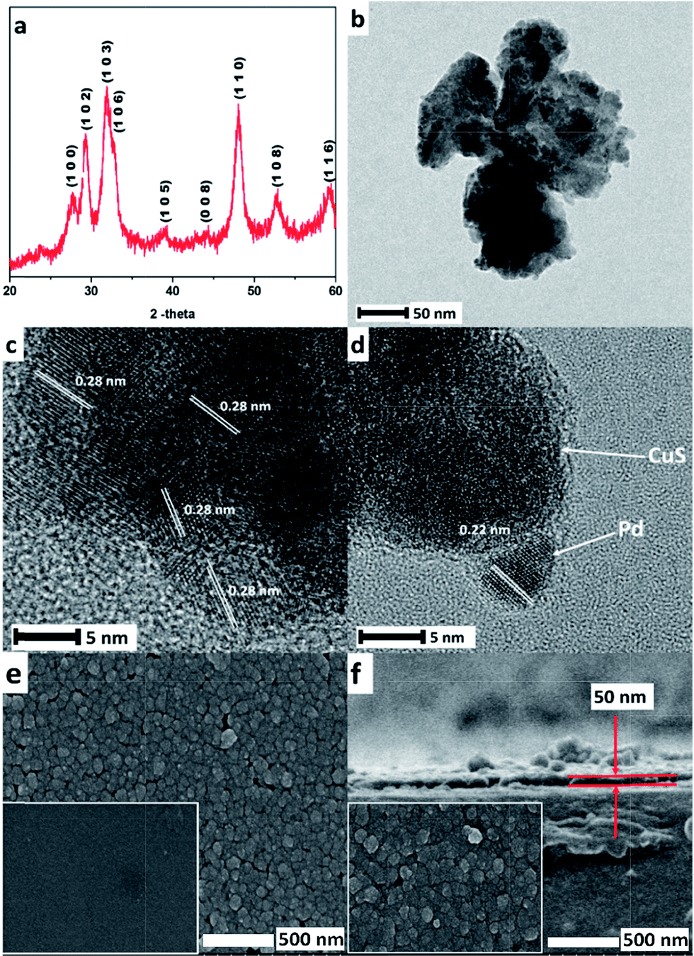 | ||
| Fig. 2 (a) XRD pattern of covellite CuS (JCPDS card 79-2321). (b) TEM image of CuS–Pd nanohybrid. (c) and (d) are the lattice-resolved TEM images of CuS and CuS–Pd, respectively. Interplanar d-spacings of 0.28 nm in (c) corresponds to the (1 0 3) lattice fringes of covellite CuS and that of 0.22 nm in (d) corresponds to the (1 1 1) lattice fringes of Pd. (e) Top view SEM image of CuS thin film on glass and inset shows the SEM image of the bare glass surface. (f) Cross-sectional SEM image of CuS–Pd thin film (50 nm) on glass and inset shows the surface of CuS–Pd thin film on glass. | ||
Pure covellite CuS is characterized by a strong free carrier absorption in the NIR region,24–27 while Cu2S and the other stoichiometric species do not show any absorption in that IR region. To investigate this, we performed UV-vis absorption measurements on the fabricated CuS thin films in the wavelength range of 300–3000 nm (Fig. S2†). The synthesized covellite CuS thin films exhibited a well-defined NIR absorption peak at around 1100 nm (Fig. S2†). This peak was ascribed to the in-plane LSPR mode, which dominates the plasmonic response.20 This peak is in agreement with the previously reported absorption spectra for pure covellite CuS (ref. 20) and confirms that the CuS thin films prepared in our study are the crystalline form of pure covellite CuS.
The as-prepared CuS films appeared semi-transparent and dark green in color. Upon exposure to H2 gas at room temperature, the color of the CuS–Pd film changed from dark green to brown. The inset of Fig. 3a shows the digital image (without applying any image processing) of the CuS–Pd film on glass substrate before and after exposure to H2 gas. In the presence of 100% H2 gas, a complete change in color is observed, while only a slight change in color is observed in the presence of 1% H2 (equivalent to the true volume concentration of 0.8% H2 in the reactor). The response time of CuS–Pd films in the presence of 100% H2 gas is noted to be less than 20 seconds, and it is less than 1 minute in the presence of 1% hydrogen after H2 flow begins (see ESI† Video clip for real-time chemochromic response). The present procedure was further applied to deposit CuS thin films on flexible plastic substrates (Fig. 4a). Fig. 4b shows the digital image of the CuS–Pd film on a flexible substrate (OHP sheet) before and after exposure to H2. A significant change in color is observed after exposure to H2 gas. This shows an additional application of the proposed synthesis method for the fabrication of flexible gasochromic sensors.
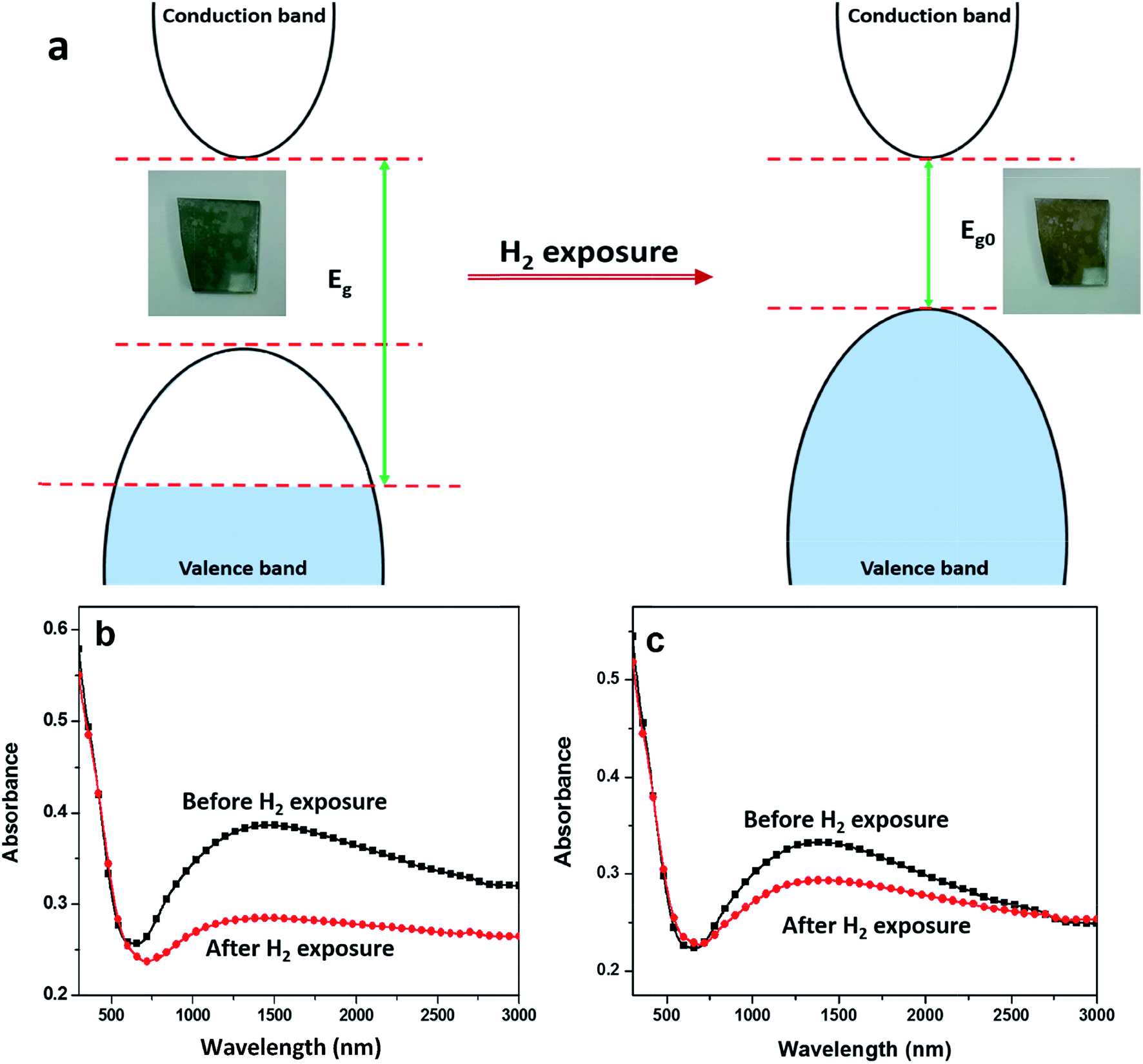 | ||
| Fig. 3 (a) Band diagram of CuS–Pd system before and after exposure to hydrogen gas. The insets are digital images showing the change in color of CuS–Pd thin films before and after exposure to hydrogen gas (dark green to brown). Absorbance spectra of CuS–Pd films before (black line) and after (red line) exposure to (b) 100% and (c) 0.8% hydrogen gas. | ||
 | ||
| Fig. 4 (a) Digital image of CuS thin film on a flexible plastic substrate (OHP sheet). (b) Digital images of CuS–Pd nanohybrid on an OHP sheet before and after exposure to hydrogen gas. (c) Absorbance and (d) transmittance spectra of CuS–Pd nanohybrid before and after exposure to hydrogen gas. | ||
Covellite CuS has strong p-type metallic character with the highest concentration of free carriers in the copper sulfide class of materials. Therefore, covellite CuS are particularly characterized by a strong free carrier absorption in the NIR region (Fig. S2†). CuS has a hole density of about 1021 cm−3, which sets its LSPR energy in the NIR range. However, in the case of stoichiometric Cu2S, the valence band is completely filled, and therefore it does not show absorption in the NIR region. Therefore, the LSPR absorption peak tends to change with a change in the free carrier concentration. Fig. 3b and c depict the absorption spectra of the CuS–Pd thin films on glass in the presence and absence of H2 gas in the wavelength range of 300–3000 nm. It is clear from the absorption spectra of CuS–Pd that a significant decrease in the absorbance is observed in the wavelength range of 1100–2500 nm after exposure to H2 gas. This decrease in LSPR was attributed to the decrease in the hole density in the valence band of the CuS system (Fig. 3a). This optical property is similar to that of Cu2S, in which the valence band is completely filled, and thus it does not show an LSPR peak in the NIR range.
Fig. S3a and b† show the transmittance spectra of CuS–Pd thin films in the presence and absence of 100% and 0.8% hydrogen in the wavelength range of 300–3000 nm, respectively. A significant change in the transmittance spectra was observed after exposure to 100% and 0.8% H2 gas. This shows the sensitivity of the CuS–Pd sensor towards hydrogen gas. Therefore, a most promising optical H2 sensor can be fabricated using CuS–Pd, which operates in transmittance mode using plastic collimating lenses. The absorption and transmittance spectra of the CuS–Pd thin films on OHP sheet in the presence and absence of hydrogen in the wavelength range of 300–3000 nm are shown in Fig. 4c and d. Significant changes in the absorption and transmittance spectra were observed after exposure to hydrogen gas, which shows an additional application as a flexible H2 sensor. The change in color or optical properties of the CuS–Pd thin films upon H2 exposure was noted to be dependent on time. Fig. S4† shows the response time of the sensor at different concentrations of H2 gas. The sensitivity of the proposed CuS–Pd sensor was compared with the other materials reported as gasochromic and optical H2 sensors. Table 1 summarizes the detection sensitivity of the present method compared with the previously reported hydrogen sensors.
| Material | Type of sensor | Sensitivity/hydrogen detection limit | Reference |
|---|---|---|---|
| Y | Gasochromic/optical | 0.1% H2 | 1 |
| Au–Pd | Gasochromic/optical | 2% H2 | 31 |
| Y–Mg alloys | Gasochromic/optical | 0.25% H2 | 32 |
| V2O5 | Gasochromic | 10% H2 | 33 |
| Palladium doped peroxopolytungstic acid | Gasochromic | 4% H2 | 34 |
| CuS–Pd | Gasochromic/optical | 0.8% H2 | Present study |
Based on our experimental results and observations, we propose a probable H2 sensing mechanism for CuS–Pd. When CuS–Pd thin film is exposed to H2 gas, H2 molecules are absorbed on Pd, which then dissociate into hydrogen atoms on the surface of Pd. These dissociated hydrogen atoms may transfer onto the surface of CuS layer by spillover and are injected into the bodies of CuS; thus, reducing the hole density in the valence band of CuS. This was evident from the significant decrease of the LSPR peak in the NIR region, as shown in Fig. 4c and d. To identify the chemical status of elemental Cu in the samples, X-ray photoelectron spectroscopy (XPS) was carried out. Fig. 5a shows the XPS of Cu profile in the samples before and after exposure to H2 gas. The shakeup line in the XPS of elemental Cu between 943 and 945 and an asymmetric tail (black line in Fig. 5), already known for covellite CuS, represents the density of the free holes in CuS.20,28 This asymmetric tail was gradually reduced in the samples after exposure to H2 (red line in Fig. 5); this reveals a decrease in the density of the free holes in CuS valence band,20 which is in agreement with the absorbance data of CuS–Pd before and after exposure to H2 gas. It has been reported that hydrogen strongly affects the electronic and structural properties of materials by binding to anions/cations (in semiconductors) or defects or other impurities.29 According to Van de Walle et al.,29 hydrogen exhibits qualitatively different behavior depending on the host into which it is introduced. Thus, it can act either as a donor (H+) or an acceptor (H−) depending on the material. In particular, when hydrogen gas is introduced into semiconductors, hydrogen binds to the anionic species in p-type material, whereas it binds to the cationic species in n-type material.29 Because CuS is a p-type semiconductor, it can be concluded that the hydrogen is assumed to bind to sulfide species in the CuS–Pd system. In CuS, the top of the valence band has a strong contribution from the sulfur p-orbitals and the bottom of the conduction band has contributions mainly from the Cu 4s and 4p orbitals.30 Therefore, hydrogen binding to sulfide species mainly affects the valence band in the CuS system. This is in agreement with the absorbance and XPS data of Cu, which shows that the hole density in the valence band of CuS is mainly affected by the presence of hydrogen contributed from sulfur. Interesting changes were also observed in the S 2p region of the XPS. A typical S 2p binding state (Fig. 5b, black curve) in covellite CuS is characterized by “three peaks”.20 Deconvolution to subcomponents (Fig. S5†) revealed the presence of two main doublets, which are characteristic of the sulfide moiety at the binding energy of 161.5 ± 0.1 eV (peak 1 in Fig. S5a†) and disulfide moiety at 162.3 ± 0.1 eV (peak 2 in Fig. S5a†) in covellite. After hydrogen gas exposure, the intensity ratio between the disulfide and sulfide components gradually decreased. Thus, the peak intensity of the sulfide moiety at 161.5 (peak 1 in Fig. S5b†) increased, while that of the disulfide moiety at 162.3 (peak 2 in Fig. S5b†) decreased. This indicates that the average −1 valency of S of covellite gradually evolved to −2 (ref. 20) after exposure to hydrogen. Based on our results, a probable sensing mechanism is proposed, as shown in Fig. 5c.
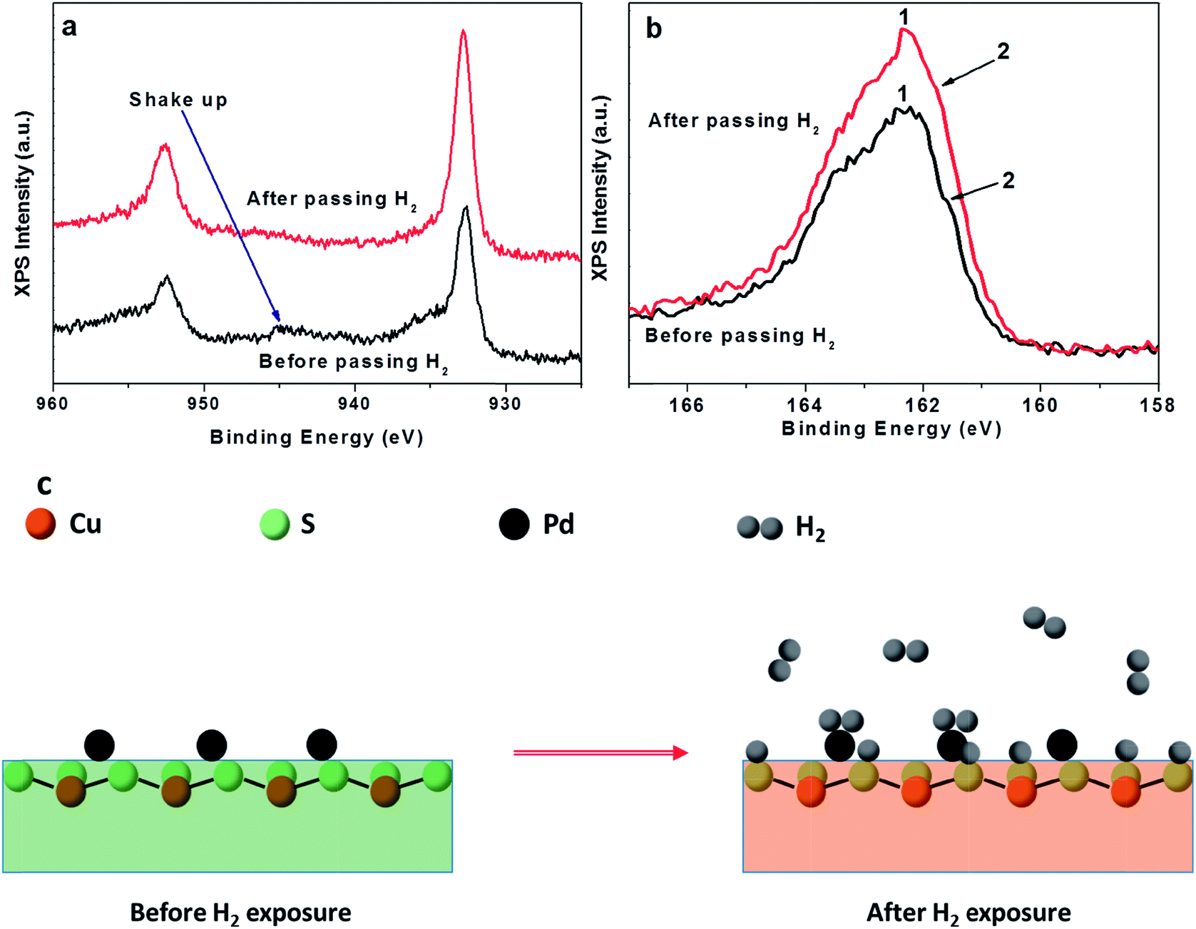 | ||
| Fig. 5 High resolution XPS characterization of CuS–Pd nanohybrid films on glass in (a) Cu 2p region and (b) S 2p region. (c) Probable hydrogen sensing mechanism of CuS–Pd nanohybrid film. | ||
The eye-readable H2 chemochromic effect in CuS–Pd is irreversible or does not recover with time in air. This ensures CuS as a discriminated class of H2 chemochromic materials from all the other oxide-based materials, which are reversible due to oxygen re-adsorption in air. It will be greatly useful for the first-level H2 leakage detection, for example, in a massive H2 delivery pipeline. We have investigated the stability of the CuS–Pd samples over a period of 5 months. For this analysis, 5 set of samples were prepared and tested for their chemochromic effect at different days. The samples were kept open to air in a laboratory atmosphere. When exposed to H2 gas, the films showed an appreciable change in color (dark green to brown), which was observed to be irreversible over the tested period (Fig. S6†). In addition, the stability of the CuS–Pd bonding was further tested by measuring TEM after hydrogen exposure. Fig. S7† illustrates the TEM image of the CuS–Pd system after hydrogen exposure, which shows significant binding even after hydrogen exposure. To test the selectivity of the CuS–Pd thin films in hydrogen sensing applications, we carried out selectivity experiments in the presence of CO and methane gases. Fig. S8† shows the photographic image and optical characteristics of the CuS–Pd thin films in the presence of CO and methane gases. CuS–Pd thin films did not show any visible change in color or absorbance or transmittance in the presence of only CO and methane gas. However, the H2 sensing properties of CuS–Pd thin films were noticeably changed in the presence of CO and methane (Fig. S8†). In the presence of CO, the H2 sensing properties were noticeably decreased, while in the presence of methane gas the sensing property was enhanced. Therefore, although individually CO or methane did not react with CuS, it is suggested that these gases may affect the H2 adsorption properties of Pd nanoparticles. A change in color and optical properties of the CuS–Pd thin films in the presence of CO, methane and H2 indicates the good selectivity of the proposed sensor.
Conclusions
An efficient and cost-effective chemochromic and optical H2 sensor has been introduced based on a CuS–Pd thin film. A change in the color/optical properties of the CuS–Pd nanostructured thin films upon exposure to H2 allows us to create eye-visible effects, making it a new gasochromic sensor in this class. Based on our experimental results, it was concluded that H2 gas interacts and binds with sulfur in the CuS–Pd system; thus, decreasing the hole density in the CuS valence band, which in turn effects the LSPR properties of CuS. The proposed gasochromic CuS–Pd film can detect up to 0.8% H2 gas in air. In addition, the present method for the deposition of CuS thin films on glass/flexible plastic substrates makes the proposed technique cost-effective and feasible for large-scale production. The present work also opens new possibilities of using copper sulfide based materials for H2 sensing applications.Acknowledgements
This work was supported by Hyundai Motors Industry-University Research Program, the Basic Science Program (NRF-2012R1A1A1005014) through the National Research Foundation (NRF) funded by MEST, ICT and Future Planning, Republic of Korea, and by the Basic Science Program (NRF-2009-0094046) through NRF funded by the Ministry of Education, Republic of Korea. Postdoctoral Fellowship awarded to S.K. was funded by BK-plus programme.References
- N. Peter, R. Tsveta, S. Martin, J. W. Ruud, S. Herman and D. Bernard, Adv. Funct. Mater., 2014, 24, 2374–2382 CrossRef.
- K. J. Liekhus, I. A. Zlochower, K. L. Cashdollar, S. M. Djordjevic and C. A. Loehr, J. Loss Prev. Process Ind., 2000, 13, 377–384 CrossRef.
- P. A. Szilagyi, R. J. Westerwaal, R. van de Krol, H. Geerlings and B. Dam, J. Mater. Chem. C, 2013, 1, 8146–8155 RSC.
- T. Hübert, L. Boon-Brett, G. Black and U. Banach, Sens. Actuators, B, 2011, 157, 329–352 CrossRef PubMed.
- X. Q. Zeng, Y. L. Wang, H. Deng, M. L. Latimer, Z. L. Xiao, J. Pearson, T. Xu, H. H. Wang, U. Welp, G. W. Crabtree and W. K. Kwok, ACS Nano, 2011, 5, 7443–7452 CrossRef CAS PubMed.
- J. Lee, W. Shim, E. Lee, J. S. Noh and W. Lee, Angew. Chem., Int. Ed., 2011, 50, 5301–5305 CrossRef CAS PubMed.
- C. McDonagh, C. S. Burke and B. D. MacCraith, Chem. Rev., 2008, 108, 400–422 CrossRef CAS PubMed.
- R. R. J. Maier, B. J. S. Jones, J. S. Barton, S. McCulloch, T. Allsop, J. D. C. Jones and I. Bennion, J. Opt. A: Pure Appl. Opt., 2007, 9, S45 CrossRef CAS.
- C. Perrotton, N. Javahiraly, M. Slaman, B. Dam and P. Meyrueis, Opt. Express, 2011, 19, A1175–A1183 CrossRef CAS PubMed.
- M. A. Butler, Appl. Phys. Lett., 1984, 45, 1007–1009 CrossRef CAS PubMed.
- M. Yang, Z. Yang, J. Dai and D. Zhang, Sens. Actuators, B, 2012, 166–167, 632–636 CrossRef CAS PubMed.
- M. H. Yaacob, J. Yu, K. Latham, K. Kalantar-zadeh and W. Wlodarski, Sens. Lett., 2011, 9(15), 16–20 CrossRef CAS PubMed.
- R. Yatskiva, J. Gryma, K. Zdanskya and K. Piksovab, Carbon, 2012, 50, 3928–3933 CrossRef PubMed.
- J. Lee, D. H. Kim, S. Hong and J. Y. Jho, Sens. Actuators, B, 2011, 160, 1494–1498 CrossRef CAS PubMed.
- Z. Wang, Z. Li, T. Jiang, X. Xu and C. Wang, ACS Appl. Mater. Interfaces, 2013, 5, 2013–2021 CAS.
- H. Huang, H. Gong, C. L. Chow, J. Guo, T. John-White, M. S. Tse and O. K. Tan, Adv. Funct. Mater., 2011, 21, 2680–2686 CrossRef CAS.
- A. Kumara, P. Zhang, A. Vincenta, R. McCormack, R. Kalyanaramane, H. J. Cho and S. Seala, Sens. Actuators, B, 2011, 155, 884–892 CrossRef PubMed.
- U. Lange, T. Hirsch, V. M. Mirsky and O. S. Wolfbeis, Electrochim. Acta, 2011, 56, 3707–3712 CrossRef CAS PubMed.
- A. R. Patrícia, D. Nicola, G. L. Salvatore, B. Seunghwan, E. C. Donato, N. Giovanni and P. Nicola, Angew. Chem., Int. Ed., 2012, 51, 11053–11057 CrossRef PubMed.
- Y. Xie, A. Riedinger, M. Prato, A. Casu, A. Genovese, P. Guardia, S. Sottini, C. Sangregorio, K. Miszta, S. Ghosh, T. Pellegrino and L. Manna, J. Am. Chem. Soc., 2013, 135, 17630–17637 CrossRef CAS PubMed.
- Y. Zhao, H. Pan, Y. Lou, X. Qiu, J.-J. Zhu and C. Burda, J. Am. Chem. Soc., 2009, 131, 4253–4261 CrossRef CAS PubMed.
- M. D. Kate, G. Franz and W. H. Thomas, Langmuir, 1999, 15, 6637–6642 CrossRef.
- C. M. Simonescu, L. Patron, V. S. Teodorescu, M. Brezeanu and C. Capatina, J. Optoelectron. Adv. Mater., 2006, 8, 597–600 CAS.
- M. C. Brelle, C. L. Torres-Martinez, J. C. McNulty, R. K. Mehra and J. Z. Zhang, Pure Appl. Chem., 2000, 72, 101–117 CrossRef CAS.
- E. J. Silvester, F. Grieser, B. A. Sexton and T. W. Healy, Langmuir, 1991, 7, 2917–2922 CrossRef CAS.
- I. Grozdanov and M. Najdoski, J. Solid State Chem., 1995, 114, 469–475 CrossRef CAS.
- K. V. Yumashev, P. V. Prokoshin, A. M. Malyarevich, V. P. Mikhailov, M. V. Artemyev and V. S. Gurin, Appl. Phys. B: Lasers Opt., 1997, 64, 73–78 CrossRef CAS.
- J. Ghijsen, L. H. Tjeng, J. van Elp, H. Eskes, J. Westerink, G. A. Sawatzky and M. T. Czyzyk, Phys. Rev. B: Condens. Matter Mater. Phys., 1988, 38, 11322–11330 CrossRef CAS.
- C. G. Van de Walle and J. Neugebauer, Nature, 2003, 423, 626–628 CrossRef CAS PubMed.
- E. J. D. Garba and R. L. Jacobs, Physica B+C, 1986, 138, 253–260 CrossRef CAS.
- M. E. Nasir, W. Dickson, G. A. Wurtz, W. P. Wardley and A. V. Zayats, Adv. Mater., 2014, 4, 3532–3537 CrossRef PubMed.
- T. Radeva, P. Ngene, M. Slaman, R. Westerwaal, H. Schreuders and B. Dam, Sens. Actuators, B, 2014, 203, 745–751 CrossRef CAS PubMed.
- W.-L. Jang, Y.-M. Lu, Y.-R. Lu, C.-L. Chen, C.-L. Dong, W.-C. Chou, J.-L. Chen, T.-S. Chan, J.-F. Lee, C.-W. Pao and W.-S. Hwang, Thin Solid Films, 2013, 544, 448–451 CrossRef CAS PubMed.
- B. Orel, N. Grošelj, U. Opara Krašovec, M. Gabršček, P. Bukovec and R. Reisfeld, Sens. Actuators, B, 1998, 50, 234–245 CrossRef CAS.
Footnote |
| † Electronic supplementary information (ESI) available: SEM-EDS data, UV-vis spectra, XPS data with peak deconvolution, sensor aging test results, and video clip for the real time sensing performance. See DOI: 10.1039/c4ra11067f |
| This journal is © The Royal Society of Chemistry 2015 |