
Particle clustering during pearl chain formation in a conductive-island based dielectrophoretic assembly system
Haitao Ding†
,
Weiyu Liu†,
Yucheng Ding,
Jinyou Shao*,
Liangliang Zhang,
Peichang Liu and
Hongzhong Liu
Micro- and Nano-manufacturing Research Center, State Key Laboratory for Manufacturing Systems Engineering, Xi'an Jiaotong University, Xi'an, Shaanxi 710049, China. E-mail: jyshao@mail.xjtu.edu
First published on 11th December 2014
Abstract
A dielectrophoretically (DEP) assembled metal nanoparticle chain can serve as an electrical connector between small conductive elements in wet electronics or as a sensing element for chemical and biological substances. Obviously, the morphology of the nanoparticle assembled chain has a strong influence on electrical conductance and surface area of this connector. This paper presents an experimental discovery that as a connection of the electrode pair to an initially isolated conductive island is formed by the assembled nanoparticle chain, an abundance of particle clusters can also be generated, which tend to accumulate on the edge of the conductive structures under certain conditions. These particle clusters either can have an undesirable impact on consistency in electrical conductance of the electric circuit or can be used to enhance the susceptibility of the sensors due to an increased surface area. Therefore, exploration is also made for manipulating and assembling metallic nanoparticles on the surface or edge of a conductive island by changing the AC frequency in the conductive island based DEP assembly system. In order to develop an explanation of the experimental observations, numerical simulation is performed to investigate the combined influence of DEP force and electrothermal flow on individual nanoparticles by taking account of the near-field effect due to particle–solid interaction or particle–particle interaction.
1 Introduction
Manipulation and assembly of low-dimensional nanostructures (usually made by chemical synthesis) in an exactly designated area is becoming a hot topic mainly due to the rapid development of nanotechnology since this capability constitutes a promising building block for various nano devices.1 Using excitation by an AC electrical field, metal nanoparticles suspended in an aqueous medium can be assembled by dielectrophoresis into patterned pearl chains (in the form of micro- or nano-sized wires) which usually have good ohmic conductance.2–5 The ability to form these electrically functional wires consistently can find potential applications in wet electronics, and molecular and chemical sensors due to the good electrical conductance and a high susceptibility and selectivity of these wires to surrounding biochemical substances.6Dielectrophoresis (DEP) is a net force exerted by a non-uniform electric field on a polarizable object suspending in a liquid medium.7 In the last few decades, DEP has been explored as an approach for manipulating micro- or nano-sized objects such as nanoparticles,8–13 DNA,14–16 cells,17–20 bacteria,21 and viruses.22 Hermanson et al. showed that isolated conductive objects such as a conductive island located between an electrode pair caused the suspending nanoparticles to chain dielectrophoretically into electrically functional wires,23,24 which can finally interconnect these isolated conductive objects. Obviously, the morphology of the assembled nanoparticle wires plays a significant role in determining the electric conductance and surface area of these connection, therefore influences the physical performance or consistency of electric circuit or sensors as a whole.23 Most researchers have so far been focused on the formation of these connective wires.23–25 However, as has been observed in this work, after the nanoparticle chained wire connecting the electrode pair to the conductive island is completed, there can be an abundance of particle clusters accumulated on the edge of the conductive structures under certain conditions, which either has an undesired impact on electric conductance of the nanoparticle chained wire on one hand or is useful for potential applications in bioassay, chemical sensing, and optical surface plasmon resonance for the pressing miniaturization trend of lab-on-chip device. Therefore, it is of significance to look into the controlled dielectrophoretic deposition pattern of nanoparticles in the vicinity of the island structure under different experimental conditions.
In this paper, the potential capability for manipulation and assembly of metallic nanoparticles on the surface or edge of a conductive island at different AC frequency is demonstrated in a conductive-island based DEP experiment. In order to gain a further understanding of the experimental observation in our DEP nanoparticle assembly system, such as accumulation of particle clusters, spatial separation of particle clusters and alternative embedding of longer particle clusters and shorter particle clusters along the island edge, a numerical simulation are performed by a combination of AC electrokinetics and electrohydrodynamics (EHD).
2 Experimental section
In this experiment, electrodes and conductive island were fabricated together on Si/SiO2 wafer with conventional optical lithography and a typical metal lift-off technique. The metal films consisted of 10 nm-thick chromium as an adhesion-enhancing layer and 90 nm thick platinum as electrodes, both deposited by magnetron sputtering. Fig. 1 shows the experimental set-up design where a pair of sharp-tipped electrodes and a diamond-shaped conductive island were used. The gap between the electrode and the island was 10 μm, while the width for the electrodes and conductive island were both 20 μm.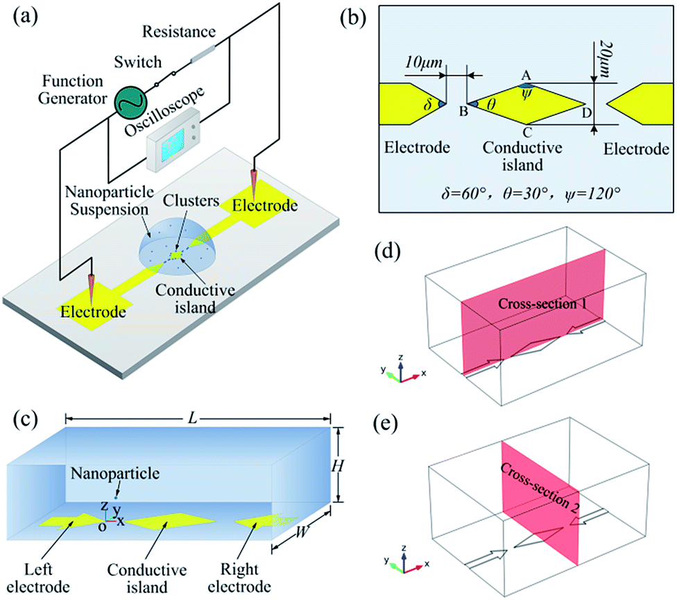 | ||
| Fig. 1 (a) Schematic experimental set-up of the conductive island based DEP process; (b) size and shape of electrodes and conductive island; (c) a schematic representation of the computational domain of the 3D numerical model for calculation of electric field, DEP velocity, thermal diffusion and ETF; (d) and (e) two cross-sections used to characterize particle behaviors are shown as well. | ||
In our experiment, a colloidal suspension of 10 nm gold nanoparticle, obtained from BBI (British Biocell International) was used. A hydrophobic ring between the electrodes is created by a liquid blocker pen to confine the droplet volume within this region. As illustrated in Fig. 1(a), a 3 μl droplet of the colloidal suspension was dripped over the electrode gap using a microsyringe. A harmonic voltage of 10 V with a frequency ranging from 100 kHz to 1 MHz, supplied from a function generator (Agilent 33220A), was applied to the electrodes via a pair of needle-shaped microprobes on a vacuum-pump based microprobing station (Wentworth Laboratories MP1008). Under an influence of the AC field, the gold nanoparticles tend to assemble directionally and form linear aggregates along the electric field lines in the gap between these conductive elements.
The microelectrode pair was connected in series with a resistor of 5 kΩ to protect the formed nanoparticle wire from being heavily melted due to the electric current passing through it once it short-circuits the electrode pair. The output voltage of the microprobe pair in contacting with the electrodes was monitored in an oscilloscope (Tektronix TDS 220). When the nanoparticles bridged the inter-electrode regions, the voltage monitored on the oscilloscope would experience a sharp drop, which was used to trigger a turning-off of the function generator. Then the sample was washed in deionized water and dried out with a nitrogen gas flow.
3 Results and discussions
3.1 Experiment observations
Fig. 2(a) is the SEM image showing a dielectrophoretically controlled assembly of 10 nm gold nanoparticles at a frequency of 100 kHz. A dominating portion of the nanoparticles is patterned into chains to form the bridges connecting the electrodes to the conductive island, while at the same time a small number of particles are dragged onto the surface of the conductive island.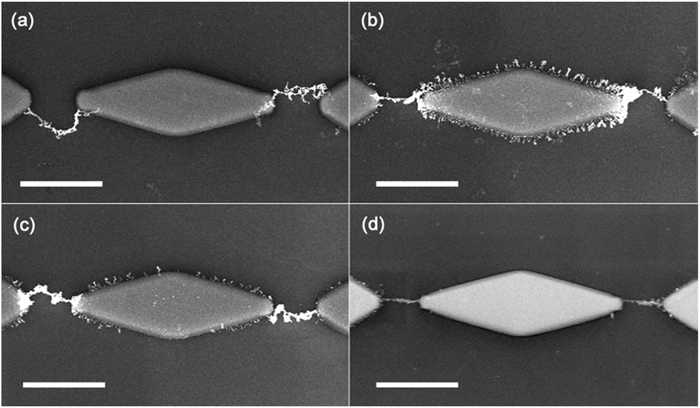 | ||
| Fig. 2 Experimental results of dielectrophoretic assembly of 10 nm gold nanoparticles at various AC frequencies: (a) 100 kHz; (b) 150 kHz; (c) 350 kHz; (d) 1 MHz. Scale bars: 20 μm. | ||
Fig. 2(b) shows experiment result at an AC field of 20 Vpp and 150 KHz. After nanoparticle wire connecting the electrode to the conductive island formed completely, there is an abundance of particle clusters accumulated on the edge of the island. The particle clusters are aligned perpendicular to the conductive island edge and keep some distance from each other. It is noted that the wire shaped particle clusters collected on the island edge have different length scales, particle clusters with longer length are separated from their neighboring companions with the same length by several shorter particle clusters (Fig. 3).
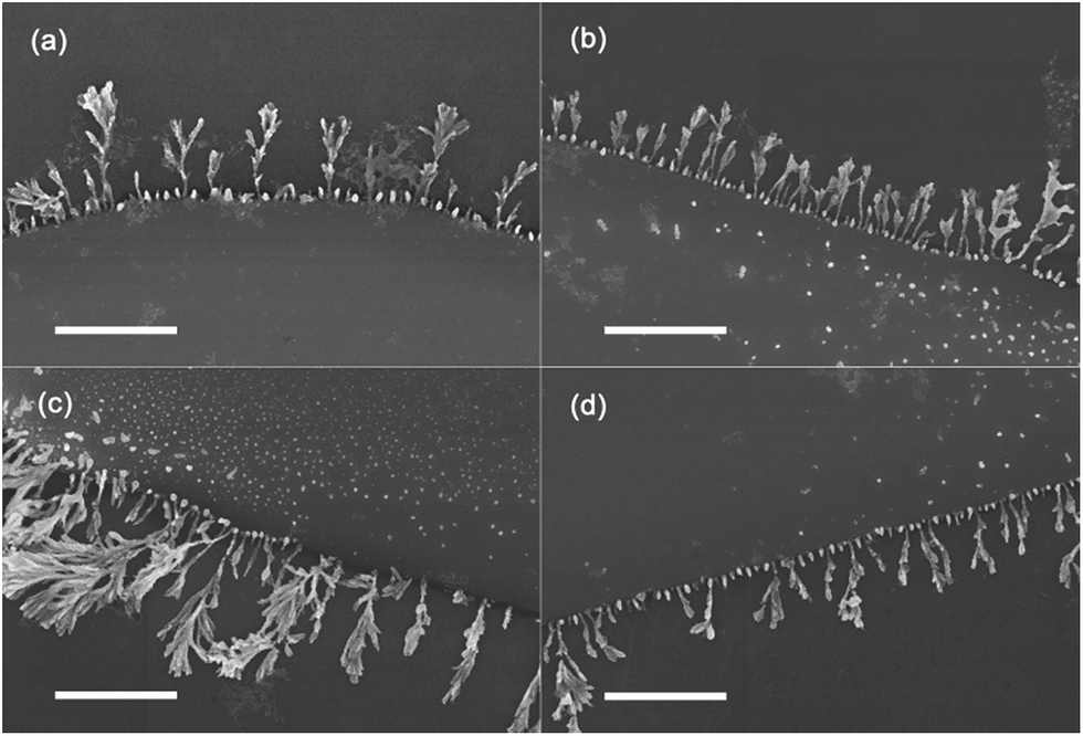 | ||
| Fig. 3 Magnified details for assembled nanoparticle clusters grown on the conductive island edge for 150 kHz at different positions: (a) island ψ corner; (b) along AD edge; (c) along BC edge; (d) along CD edge. The island edges are labeled in Fig. 1(b). Scale bars: 2 μm. | ||
At 350 kHz, as seen from Fig. 2(c), it takes more time for a formation of the nanochains to completely short-circuit the microelectrode system than at 150 kHz. Besides, much fewer particle clusters has settled down on the island edge as compared to those at 150 kHz.
At 1 MHz, a relatively long time is required for nanoparticle wires to totally bridge the microelectrode system, hardly any particle clusters is populated on the island edge or surface and the bridging nanoparticle wires tend to be better-shaped, as shown in Fig. 2(d).
In order to explain the observations in our experiments, a series of numerical modeling is conducted to reveal the underlying mechanisms that lead to the observed particle motion based on theory of dielectrophoresis and AC electrohydrodynamic flow.
3.2 Particle dieletrophoresis
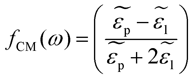
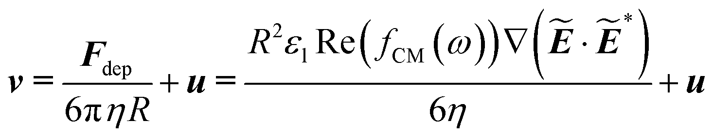
Free charge can be induced at the interface of two dielectric mediums of different charge relaxation time due to the action of Maxwell Wagner interfacial polarization effect. Particle dielectrophoresis depends on the mismatch between dielectric properties of the particle and the used liquid suspension. For a spherical particle of radius R suspended in a fluid subjected to a local non-uniform electric field E, the time-averaged dielectrophoretic force Fdep can be obtained from point dipole (PD) approximation in the absence of any near field effect26| Fdep = πεlR3Re(fCM(ω))∇(Ẽ·Ẽ*) | (1) |
 | (2) |
 and
and  are the complex permittivity of the nanoparticle and liquid medium respectively, i.e.
 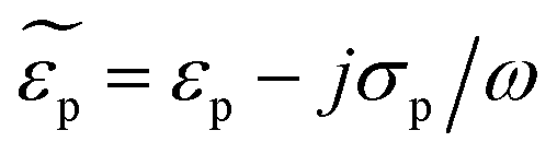 ,
, 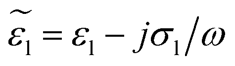 , with εp = εo and εl = 80εo representing the permittivity of the particle and liquid medium (εo = 8.85 × 10⁻¹² F m−1 is vacuum permittivity), σp = 0.01 S m−1 and σl = 0.0004 S m−1 denoting their electric conductivity. The frequency dependent CM factor, fCM, for the 10 nm-diameter particle is shown in Fig. 4. On one hand, if Re(fCM(ω)) > 0, particles tend to be attracted to regions of high field intensity by the external field, and this phenomenon is termed as positive dielectrophoresis (p-DEP). Otherwise, particles experience negative dielectrophoresis (n-DEP) and are repelled to regions of low field gradients.
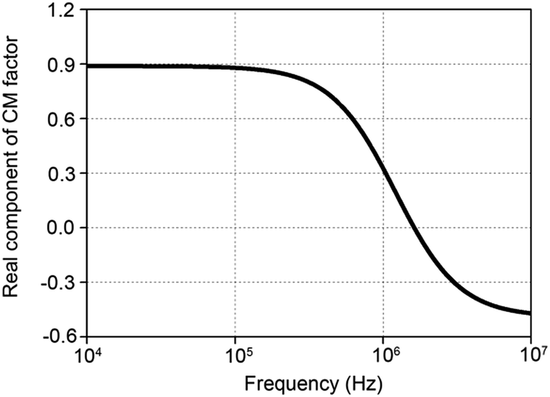 | ||
| Fig. 4 Real component of CM factor for the used 10 nm particle. | ||
In our experiments, dielectrophoretic assembly of the used 10 nm gold nanoparticles cannot be achieved once the driving frequency exceeds 2 MHz, thus the bulk conductivity σp = 0.01 S m−1 of gold particle is considered to be refrained due to a thin layer of stabilization agent coated on its surface.27 From Fig. 4, a Maxwell–Wagner relaxation frequency of interfacial charge is found around 1.6 MHz corresponding to our experimental observations very well.
In order to capture the spatial distribution of dielectrophoretic force, the electric field must be fully resolved within the device. Holding the quasi-electrostatic limit of Maxwell formulations, under the actuation of a harmonic potential difference, the governing equation of potential distribution Ṽ in frequency space is given by28
| ∇((σ + jωε)∇Ṽ) = 0 | (3) |
With Ẽ = −∇Ṽ. Where ε and σ are the dielectric permittivity and electric conductivity of the corresponding computational domain.
In typical microelectrode systems, the consideration of an individual particle moving at its terminal velocity is true due to its negligible mass inertia under such environments.
 | (4) |
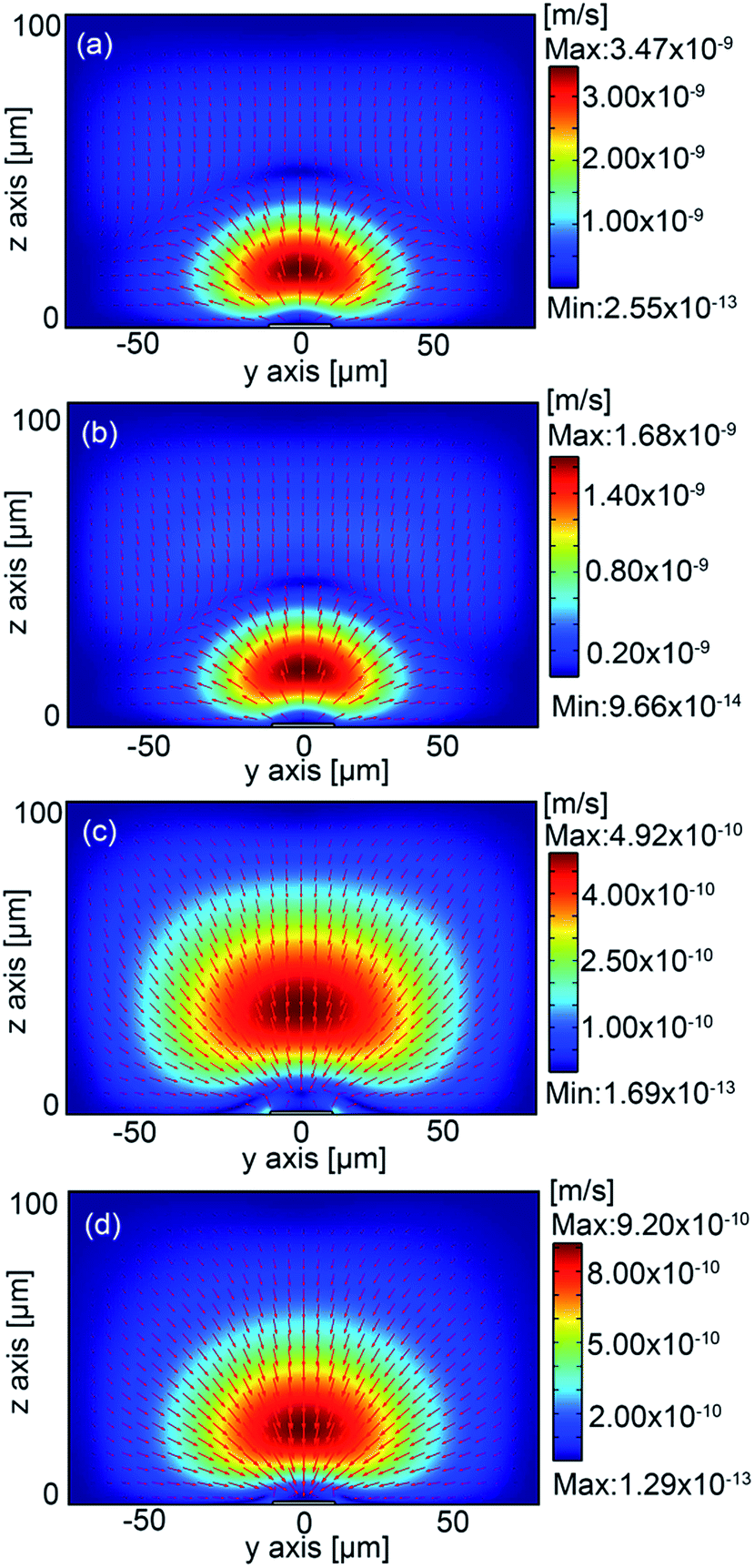
Two cross-sections most representative of particle behaviors chosen to characterize the motion of particles as well as its surrounding liquid suspension are shown in Fig. 1(d) and (e). Cross-section 1 is an x–z plane passing through both the island center line and that of electrode pair. Cross-section 2 denotes a y–z plane running across the center line of inter-electrode gap.
The spatial distribution of particle velocity induced due to the action of dielectrophoretic force at 150 kHz is shown in Fig. 5. The maximum induced DEP velocity of an individual particle is in the vicinity of the electrode tip (δ) as well as the island tip (θ) with a value of about 1 mm s−1 (Fig. 5(a)). Particles at 150 kHz experience p-DEP and are attracted to these regions of a strong field intensity as indicated by the direction vectors (Fig. 5(b)). Therefore, nanoparticles can be directionally assembled into pearl chains aligned along electric field lines due to the action of p-DEP as well as DEP interaction between neighboring particles. The average DEP velocity in the assembly region is on the order of 0.01 μm s−1. Because of a local field minimum in the middle of the island surface (Fig. 5(c)), particles are repelled from there and transported to a higher level of about 20 μm levitation from the substrate surface at which the direction of DEP force makes a change (Fig. 5(d)). Particle clusters attached to the ψ tip cannot be explained clearly until now.
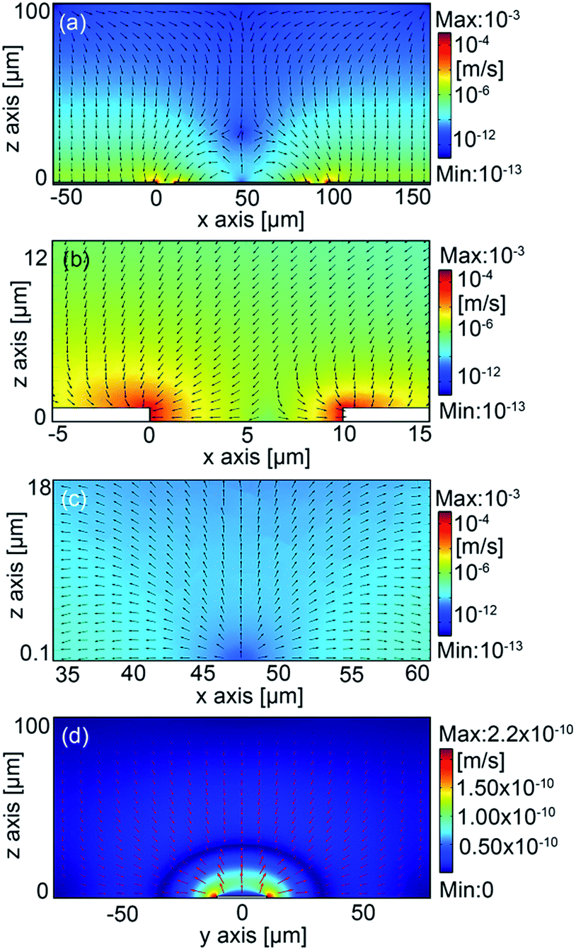 | ||
| Fig. 5 The spatial distribution of particle velocity induced due to DEP force at 150 kHz: (a) in cross-section 1; (b) in the gap between the electrode and island in cross-section 1; (c) in the middle part of island surface in cross-section 1; (d) in cross-section 2 (vectors represent the direction of DEP velocity and surface color denotes its magnitude with (a)–(c) in log scale). | ||
3.3 Electrothermal induced flow
In a typical lab-on-chip microelectrode system for manipulation and assembly of nano-sized objects, the various fluid movements due to an applied external field include AC induced electroosmosis flow and electrothermal flow (ETF) as well as Joule heating induced buoyancy flow in the absence of any external applied heat.29For the frequencies from 100 kHz to 1 MHz applied in our current DEP experiments, electroosmosis flow due to double layer charging at the electrode/electrolyte interface is negligible small. Besides, buoyancy flow is impossible to dominate over electrothermal induced flow because the characteristic length of the used microelectrode system is on the order of several tens of micrometers.30 It is thereby concluded that ETF plays most significant role on any individual particle motion besides DEP in our experiment.
ETF arises from interaction of an external non-uniform electric field with the gradients in electric properties of liquid medium subjected to a temperature gradient, which can be established from either internal Joule heating or an externally controlled heat source. In the limitation of minimum maximum temperature rise in the internal solution, the time-averaged electrothermal body force exerted on per unit volume of the fluid domainis31
 | (5) |
The two terms on right hand side of above eqn (5) represent Coulomb force and dielectric force, respectively. Coulomb force is due to charge induction in a non-isothermal electric field, and it dominates fluid behavior in the low frequency range. Dielectric force arises from the response of bound charge to external field for any anisotropic dielectric medium, and it plays major effects in determination of the fluid motion at high driving frequency.
The cross over frequency at which the fluid motion transits from being Coulomb force dominated to dielectric force dominated is32
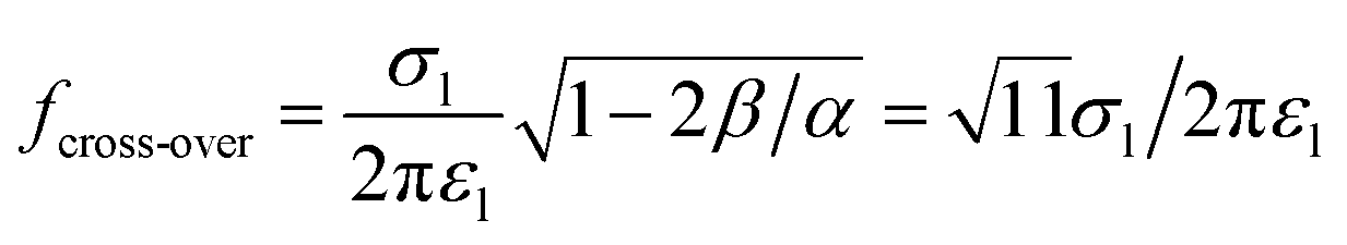 | (6) |
| fcross-over = 296 kHz. |
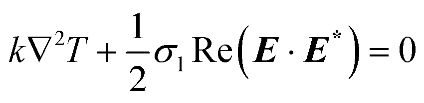
To account for these liquid inhomogeneities, the energy balance equation related to internal temperature field must be solved within the whole microelectrode device.33
 | (7) |
As for fluid transportation, the Navier–Stokes equation of an incompressible fluid at a low Reynolds number is modified to account for the electrothermal body force acting on fluid domain
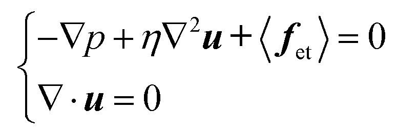 | (8) |
We solved the three sets of physical equations including potential distribution (3), thermal diffusion (7) and fluid transportation (8) in a sequential manner subjected to appropriate boundary conditions as depicted below.
A typical configuration of the 3D simulation model for potential distribution, thermal diffusion and fluid movement is shown in Fig. 1(c).
A computational domain of cubic shape with confined but enough space is considered here, L = 210 μm, W = 150 μm, H = 100 μm, such that any near field effect of the outer boundary of liquid suspension on gap regions of interest can be mitigated, thus the numerical solutions to these physical problems in the assembly region are acceptable.34 Potential phasors are prescribed on electrode pair as V = Vpp/2 = 10 V and V = 0 V respectively, with Vpp = 20 V denoting the peak-to-peak voltage applied in real experiments. Electric insulation is considered for all the other boundaries. Ambient temperature of 293.15 K is maintained on electrode pair and conductive island due to their high thermal conductivity and sufficient thickness. On the outer boundary of this liquid droplet, an adiabatic condition is preferred. A no slip wall boundary condition is assumed at all the interfaces and solid surfaces.
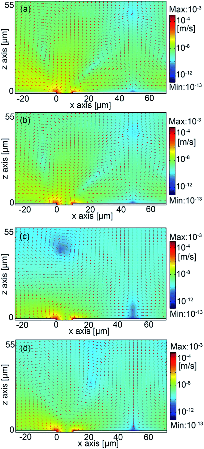
Fig. 6 shows the results of ETF simulation at various driving frequencies in terms of cross-section 1. There are four flow vortices in cross-section 1 independent of the driving frequency. However, flow reversal occurs on the order of charge relaxation frequency. For the driving frequency below 296 kHz, electrothermal induced flows stream downward above the center of the gap between the electrode and island, and sweep across the surface of the electrode/island and then go upward from the electrode/island surface to form circulating flow patterns (Fig. 6(a) and (b)). In the center of the island surface, flows in opposite directions cancel out each other and a stagnation region for particle collection is created.
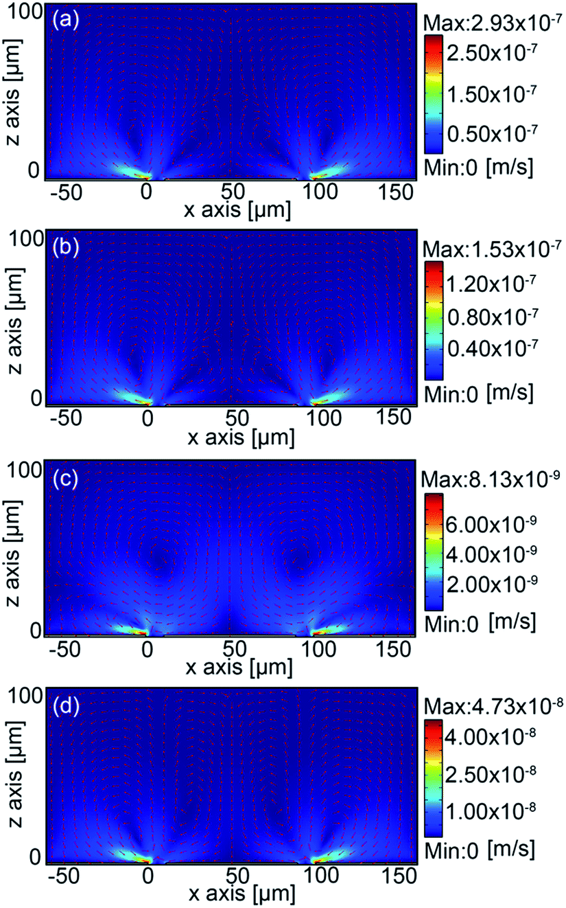 | ||
| Fig. 6 Spatial distribution of electrothermal flow in cross-section 1: (a) at 100 kHz, (b) at 150 kHz, (c) at 350 kHz and (d) at 1 MHz (surface color indicates magnitude of flow velocity together with normalized direction vectors). | ||
In the range of frequency (300 kHz–400 kHz) where the fluid transits from being Coulomb force dominated to dielectric force dominated, the magnitude of flow velocity is extremely weak (Fig. 6(c) and 7).
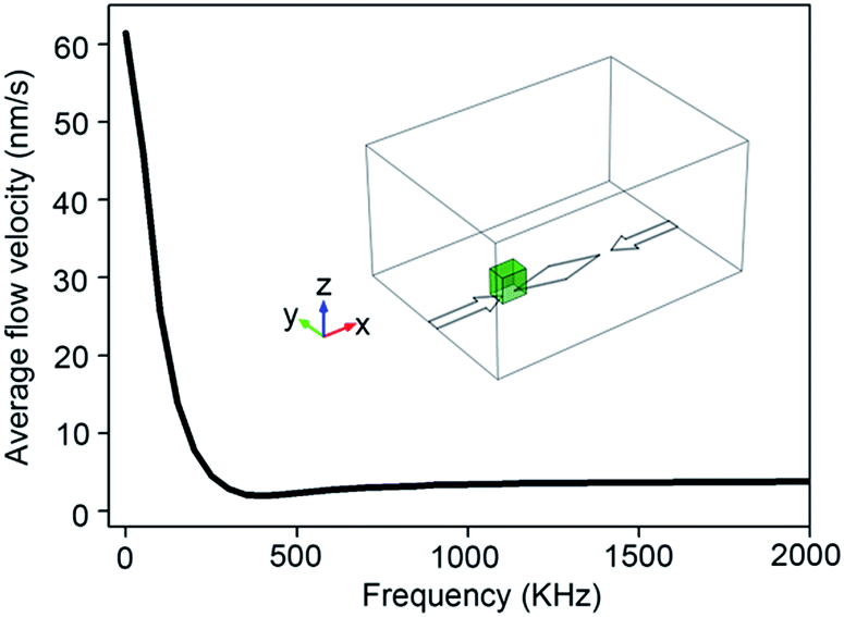 | ||
| Fig. 7 Variation of average electrothermal flow velocity with frequency in the nanoparticle assembly region represented by the green box shown at the inset. | ||
For higher frequencies, flow direction has been reversed due to the relaxation process which inhibits free charge from accumulating at the surface (Fig. 6(d)). Electrothermal vortices stream downward above the center of the island surface as well as the electrode surface, meet each other in the gap region and then dash upward above the gap resulting in closed flow loops, which leads to a cancellation of the particle cessation region established on the island surface at relatively lower driving frequencies. As a consequence, fewer particles are captured on the island edge as well as its surface at frequencies higher than 296 kHz, as has been observed in real experiments.
3.4 Resultant velocity of nanoparticle motion
A particle in an AC electrokinetic system can experience various actions, including DEP force, fluidic drag, Brownian motion, Van Der Waals force and electric bilayer interaction.35 Yet DEP force and fluidic drag is generally regarded as the most dominant driving mechanisms in an AC dielectrophoretic process, as indicated by Liu et al. in the estimation of various forces exerted on nanoparticle by an analysis of the order of magnitude.36The transporting velocity of a moving particle considering DEP force and fluidic drag is given by30
 | (9) |
The final particle movement is due to the combinational operation of any external force (DEP as considered here) induced velocity and fluid transportation effect.
From the perspective of quantitative comparisons, average fluid flow velocity in the assembly region is calculated to be 3 × 10⁻⁸ m s−1 at 150 kHz (Fig. 7), while DEP velocity magnitude reaches 9 × 10⁻⁸ m s−1 (7 × 10⁻¹⁸ N). Thus the combinational effects of ETF and DEP velocity are necessary to be investigated since they are comparable in scale in our current experiment system.
From Fig. 8, strong motion of nanoparticles are observed at the electrode tips as well as island tip in the frequency range of interest due to the action of stable p-DEP force below 1 MHz. Electrothermal induced vortex motion of liquid suspension are seen at far field region. Stagnation region on the island surface for particle collection exists in low frequency range (<296 kHz) while vanishes at high driving frequency (>296 kHz), because of flow reversal at 296 kHz. As a consequence, driving frequency more than 296 kHz is not suitable for particle collection on the island surface or edge.
 | ||
| Fig. 8 Spatial distribution of particle velocity due to the combined action of DEP force and electrothermal induced flow in cross-section 1: (a) at 100 kHz, (b) at 150 kHz, (c) at 350 kHz and (d) at 1 MHz (surface color indicates magnitude of particle velocity plotted in log scale together with normalized direction vectors). | ||
In the low frequency range, electrothermal flow carries nanoparticles to the vicinity of electrode/island tip, leaving a short time for DEP force to drag them onto the solid surface. Since magnitude of flow velocity at 150 kHz are much lower than that at 100 kHz (Fig. 7), there is more chance for DEP force to capture nanoparticles onto the island surface at 150 kHz rather than 100 kHz.
In the middle part of the island surface, DEP force just above the solid surface always attempts to repel the nanoparticles away from the island to the surrounding liquid medium irrespective of the driving frequency (Fig. 5(d)). In the low frequency range limit, electrothermal force acts in the same direction with DEP force (Fig. 6(a) and (b)) resulting in nanoparticles to be repelled from the middle part of the island surface (Fig. 9(a) and (b)). At high frequencies, ETF reverses its direction and thus tends to transport them onto the island surface and edge. However, DEP stoutly competes with this kind of attraction force in the vicinity of the solid surface and still leads to a failure in particle collection (Fig. 9(c) and (d)).
 | ||
| Fig. 9 Spatial distribution of particle velocity due to the combined action of DEP force and electrothermal induced flow in cross-section 2: (a) at 100 kHz, (b) at 150 kHz, (c) at 350 kHz and (d) at 1 MHz (surface color indicates magnitude of particle velocity together with normalized direction vectors). | ||
Based on the above analysis, particle clusters accumulated in the middle of the island edge can be attributed to the combinational action of DEP force and ETF at 150 kHz. In order to address the behavior of particle motion more explicitly, particle locus as a function of their initial position with respect to the island surface are studied.
Six particles are chosen to situate around the island with zero initial velocity (Fig. 10). These particles are spatially distributed along one island edge with a uniform interval. Particle 1 (P1) and 2 (P2) are neighboring to the island tip facing the electrode, particle 3 (P3) and 4 (P4) are in the vicinity of the middle part of the island edge, and particle 5 (P5) and 6 (P6) are proximity to the ψ tip. The behaviors of these six particles are therefore most representative. Besides, P1, P3, P5 are initially positioned at a height of 8 μm from the island surface, while P2, P4, P6 are in the island plane.
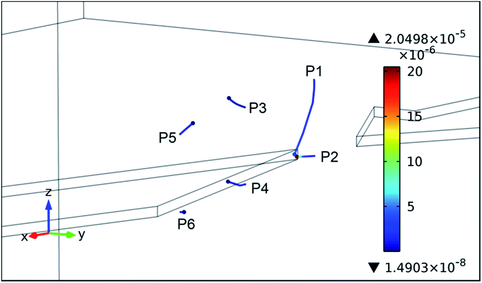 | ||
| Fig. 10 Particle trajectories due to the combined action of DEP force and electrothermal flow (surface color of the tube bar representing particle locus indicates the velocity magnitude of particle transient motion, unit: m s−1). | ||
Though P1 is located at a much higher level than P2, they are both finally embedded near the island tip. However, it merely takes about 2 seconds for P2 to reach the island edge due to its small distance to the island as compared to 500 s required by P1. As a consequence, ETF above the island tip (θ) helps DEP carry nanoparticles to the vicinity of island tip and leaves enough time for DEP to fix them permanently there.
Around the middle part of the island edge, particles at a sufficient high level tend to miss p-DEP entrapment, as indicated from the movement of P3. P3 keeps track of the flow transportation rather than DEP force vector due to the much more weakened field gradient here as compared to the island tip (θ). In the meantime, particle with a small distance to the island edge has still opportunities to be attracted onto the island as predicted by the movement of P4, since p-DEP completely dominates particle motion in the near field region over electrothermal effect, which has minimal action on an individual particle because of the no slip wall boundary condition imposed on the island surface.
For initial locations of particles adjacent to the ψ tip, both P5 and P6 are repelled from island to its surrounding regions due to a local field minimum at the ψ tip. Besides, electrothermal force works in approximately the same direction with DEP force (Fig. 6(b)). In short, particles always tend to move away from the ψ tip due to the action of the applied external field. As a result, that particle clusters accumulated around ψ tip in our experiments still remains a mystery. It is therefore necessary to introduce Maxwell stress tensor formulations to investigate near field interactions between particle and the conductive island.
3.5 Electric field induced near-field influence
Once any near field effect is present and cannot be ignored, Maxwell stress tensor (MST) is an efficient alternative to DEP force calculation. The time average DEP force in a harmonic field derived by Wang et al. is used in our MST DEP calculation37
 | (10) |
It should be noted that the influence of particles on field distribution is directly considered in MST method,38,39 which determines the intrinsic difference between MST approach and PD method.
In this model, a 10 nm gold nanoparticle is placed near the island edge as shown in Fig. 11. When the particle is fixed at a 1.5R distance to the island edge, a kind of attraction force induced by near field DEP always exists in the frequency range of interest. With increasing frequency, there is a monotonic downward trend of this attraction force (Fig. 11(a)). Therefore, it is more difficult for particles to be dragged toward the island edge due to the action of this attraction DEP force at 1 MHz than 150 kHz. Besides, this near field interaction is only attractive when vertical distance from particle center to island edge is less than 50 nm at 150 kHz. The force magnitude declines sharply with distance and becomes repulsive beyond 50 nm, which indicates near-field attraction force due to DEP vanishes when particle gets far away from the island edge. Consequently the DEP force due to the external field acting on the particle dominates the particle behavior and repels it away from the island edge (Fig. 11(b) and 5(c)). On the contrary, PD approach gives a force magnitude of 1 × 10⁻²⁰ N at 150 kHz much smaller than the attraction DEP force of 5 × 10⁻¹⁹ N from MST method when the vertical distance from the particle center is 1.5R.
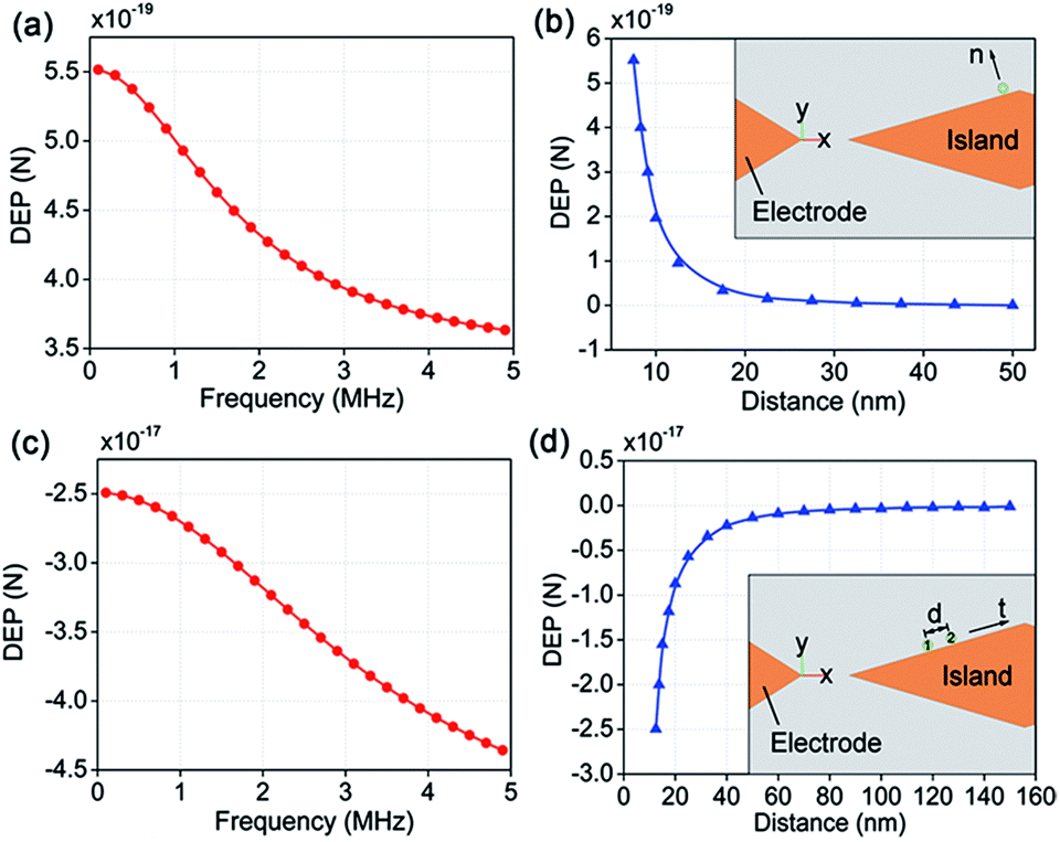 | ||
| Fig. 11 Mutual DEP force at 150 KHz: normal to the surface of island edge exerted on a particle located in the vicinity of ψ tip, (a) as a function of frequency, (b) as a function of distance; exerted on particle 1 when neighboring particles are laid near the island edge with their connecting lines parallel with island edge, (c) DEP interaction as a function of frequency, (d) DEP interaction as a function of distance between particle centers. | ||
The DEP interaction acting on a particle induced due to the presence of a neighboring particle is investigated using a similar method. The arrangement of a pair of adjacent particles marked as 1 and 2 is shown in Fig. 11(c) and (d). The distance between the particle centers is prescribed at 2.5R, frequency dependence characteristics of DEP interactions along tangential direction (t) of the surface of island edge acted on particle 1 is investigated. It is discovered DEP interaction is on the rise with a rather gentle slope as frequency increases (Fig. 11(c)). Besides, this kind of repulsion force due to DEP interaction shows a sharp monotonous decreasing trend with distance between the particle centers along the island edge. The repelling DEP interaction decreases more slowly as a function of particle distance, in comparison with the attractive DEP interaction, which implies repelling DEP interaction plays a significant role on particle behavior in a much larger length scale (Fig. 11(b) and (d)). Therefore a conceivable consequence is obtained that particle clusters accumulated on the island edge always keep a distance from each other. But why longer particle clusters and shorter particle clusters are embedded alternatively is a still mystery, which may be attributed to the complex EHD flow and electrochemical reaction during the dynamic process of particle dielectrophoretic motion. A total DEP force magnitude of 1 × 10⁻¹⁹ N from PD method at 150 kHz is about two orders of magnitude smaller than the repelling DEP interaction of 2 × 10⁻¹⁷ N from MST method at a particle distance of 2.5R.
We then deal with electric conductance characterization of the DEP-assembled microwires. In order to measure the resistances of the microwires on the sides of the conductive island, the conductance instrument is carefully applied between the electrode and the conductive island by needle probes. Since resistances of both chains branches connecting each electrode to the central island are approximately identical due to geometrical symmetry, measurement is conducted only for one branch. Fig. 12 shows the resistances of the microwires at different assembly frequencies. The frequency-dependent DC impedance can be attributed to a varying morphology of the assembled nanoparticle wires. The length and average diameter of the nanoparticle wires can be measured from the SEM graphs.
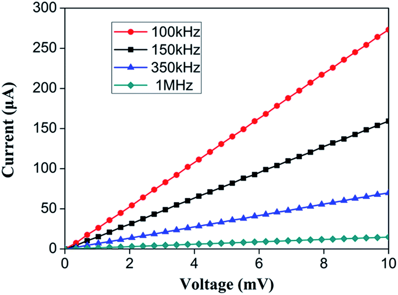 | ||
| Fig. 12 I–V characteristics of the microwires at different assembly frequencies. | ||
At 100 kHz (1 MHz), the resistance is the least (greatest) for the largest (lowest) diameter of the microwires. The diameter at 1 MHz is 200 nm, the corresponding resistivity 1.88 × 10⁻⁵ Ω m is three orders of magnitude larger than that of bulk gold, which can be ascribed to small contact areas among the nanoparticles.
Fig. 13 shows a sensing response of the microwires assemblied at 150 kHz to 2.0 × 10⁻⁴ M laurylmercaptan solution that can bring about severe pollution to the water environment. The conductance instrument is applied between the electrodes by needle probes. A 5 μl droplet of 2.0 × 10⁻⁴ M laurylmercaptan solution is dripped over the microelectrode system. The resistance increases by 15% after 5 minutes. It is concluded that the electric conductivity of the microwires would decay if the surface of the nanoparticle wires was covered by a polymer layer.
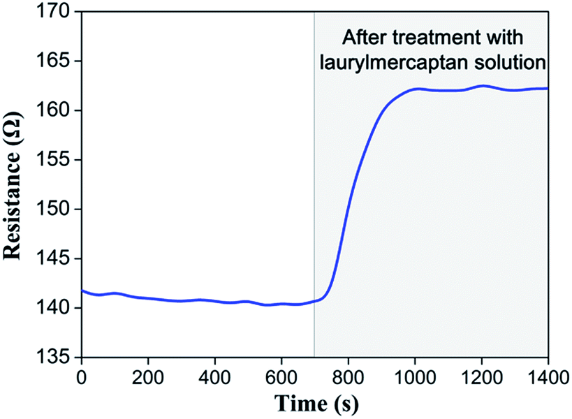 | ||
| Fig. 13 Response behaviour of the microwire detector to laurylmercaptan solution. | ||
4 Conclusions
In this study, the importance of field frequency in inducing patterning of nanoparticle clusters assembled in situ from colloidal suspension in a conductive-island based DEP experiment is investigated. The phenomena in specific range of frequency are observed, such as particle clusters accumulated, particle clusters keeping a distance from each other as well as longer and shorter particle clusters embedded alternatively along the island edge. From the viewpoint of point dipole model (PD), behaviors of a large population of particle clusters accumulated on the middle of island edge can be explained. But it fails to demonstrate particle clusters are transported to the vicinity of ψ tip and then stick there. In order to get a better interpretation of particle behaviors, MST formulations considering particle–particle and particle–island surface interactions are employed to calculate the DEP interaction due to near field effect acted on individual particles in the presence of EHD flow.The observed particle behaviors are attributed to combinational effect of DEP mechanism and electrothermal flow. Electrothermal flow plays important effect on particle behaviors in the current system. There is a stagnation region for particle collection where flow velocity is counteracted by two counter-rotating eddies in opposite directions and becomes zero. It is impossible for particle to accumulate on the island edge once direction of electrothermal flow is reversed which makes the stagnation region no longer exist. Attractive DEP interaction is proved at a particle–island distance less than 50 nm. This kind of attraction decreases with frequency and it is therefore more difficult for particle to collect on island edge. Besides, there is strong repelling interaction when a particle pair is aligned along the island edge, which explains that particle clusters always keep a certain distance with each other.
The electric conductance characterization of the DEP-assembled microwires was measured. At 100 kHz (1 MHz), the resistance is the least (greatest) for the largest (lowest) diameter of the microwires. This paper then investigates a sensing response of the microwires assemblied at laurylmercaptan solution that can bring about severe pollution to the water environment.
Consequently, this kind of conductive island based DEP microelectrode system has great potentials for applications in effective manipulation and assembly of nanoparticles to a designated region, based on a combinational effect of DEP mechanism and EHD fluidic drag.
Conflict of interest
The authors declare no competing financial interest.Acknowledgements
This work was supported financially by the NSFC Major Research Plan on Nanomanufacturing (grant no. 91323303), NSFC Funds (no. 51175417 and no. 51275401) and Shaanxi Young Talents in Science and Technology (2013KJXX-047).Notes and references
- H. Morgan and N. G. Green, AC Electrokinetics: Colloids and Nanoparticles, Research Studies Press, Herts, 2003 Search PubMed.
- R. Kretschmer and W. Fritzsche, Langmuir, 2004, 20, 11797–11801 CrossRef CAS PubMed.
- R. J. Barsotti, M. D. Vahey, R. Wartena, Y. M. Chiang, J. Voldman and F. Stellacci, Small, 2007, 3, 488–499 CrossRef CAS PubMed.
- S. I. Khondaker and Z. Yao, Appl. Phys. Lett., 2002, 81, 4613–4615 CrossRef CAS PubMed.
- A. Zoy, A. A. Nassiopoulos and A. G. Nassiopoulou, Nanotechnology, 2007, 18, 345608 CrossRef.
- J. Lee, S. Mubeen, C. M. Hangarter, A. Mulchandani, W. Chen and N. V. Myung, Electroanalysis, 2011, 23, 2623–2628 CrossRef CAS.
- P. R. C. Gascoyne and J. Vykoukal, Electrophoresis, 2002, 23, 1973–1983 CrossRef CAS.
- L. Zheng, S. Li, J. P. Brody and P. J. Burke, Langmuir, 2004, 20, 8612–8619 CrossRef CAS PubMed.
- B. C. Gierhart, D. G. Howitt, S. J. Chen, R. L. Smith and S. D. Collins, Langmuir, 2007, 23, 12450–12456 CrossRef CAS PubMed.
- O. D. Velev and K. H. Bhatt, Soft Matter, 2006, 2, 738–750 RSC.
- S. Kumar, S. H. Yoon and G. H. Kim, Curr. Appl. Phys., 2009, 9, 101–103 CrossRef PubMed.
- D. Cheon, S. Kumar and G. H. Kim, Appl. Phys. Lett., 2010, 96, 013101 CrossRef PubMed.
- S. I. Khondaker, K. Luo and Z. Yao, Nanotechnology, 2010, 21, 095204 CrossRef PubMed.
- S. Roy, H. Vedala, A. D. Roy, D. H. Kim, M. Doud, K. Mathee, H. K. Shin, N. Shimamoto, V. Prasad and W. Choi, Nano Lett., 2008, 8, 26–30 CrossRef CAS PubMed.
- H. Vedala, S. Roy, M. Doud, K. Mathee, S. Hwang, M. Jeon and W. Choi, Nanotechnology, 2008, 19, 265704 CrossRef PubMed.
- D. Porath, A. Bezryadin, S. de Vries and C. Dekker, Nature, 2000, 403, 635–638 CrossRef CAS PubMed.
- M. Yang and X. Zhang, Sens. Actuators, A, 2007, 135, 73–79 CrossRef CAS PubMed.
- R. Pethig, Crit. Rev. Biotechnol., 1996, 16, 331–348 CrossRef.
- B. M. Taff and J. Voldman, Anal. Chem., 2005, 77, 7976–7983 CrossRef CAS PubMed.
- S. Gupta, R. G. Alargova, P. K. Kilpatrick and O. D. Velev, Langmuir, 2010, 26, 3441–3452 CrossRef CAS PubMed.
- S. G. Dastider, S. Barizuddin, M. Dweik and M. Almasri, RSC Adv., 2013, 3, 26297–26306 RSC.
- B. H. Lapizco-Encinas, R. V. Davalos, B. A. Simmons, E. B. Cummings and Y. Fintschenko, J. Microbiol. Methods, 2005, 62, 317–326 CrossRef CAS PubMed.
- K. D. Hermanson, S. O. Lumsdon, J. P. Williams, E. W. Kaler and O. D. Velev, Science, 2001, 294, 1082–1086 CrossRef CAS PubMed.
- K. H. Bhatt and O. D. Velev, Langmuir, 2004, 20, 467–476 CrossRef CAS.
- H. T. Ding, W. Y. Liu, J. Y. Shao, Y. C. Ding, L. L. Zhang and J. Q. Niu, Langmuir, 2013, 39, 12093–12103 CrossRef PubMed.
- N. G. Green, A. Ramos and H. Morgan, J. Electrost., 2002, 56, 235–254 CrossRef.
- M. L. Li, Y. L. Qu, Z. L. Dong, Y. C. Wang and W. J. Li, IEEE Trans. Nanotechnol., 2008, 7, 477–479 CrossRef.
- N. G. Green, A. Ramos, A. González, A. Castellanos and H. Morgan, J. Electrost., 2001, 53, 71–87 CrossRef.
- O. D. Velev, S. Gangwal and D. N. Petsev, Annu. Rep. Prog. Chem., Sect. C: Phys. Chem., 2009, 105, 213–246 RSC.
- A. Castellanos, A. Ramos, A. González, N. G. Green and H. Morgan, J. Phys. D: Appl. Phys., 2003, 36, 2584–2597 CrossRef CAS.
- R. M. Zhang, C. Dalton and G. A. Jullien, Microfluid. Nanofluid., 2011, 10, 521–529 CrossRef.
- M. Lian, N. Islam and J. Wu, IET Nanobiotechnol., 2007, 1, 36–43 CrossRef CAS.
- F. J. Hong, J. Cao and P. Cheng, Int. Commun. Heat Mass Transfer, 2011, 38, 275–279 CrossRef PubMed.
- A. K. Naieni and A. Nojeh, Nanotechnology, 2012, 23, 495606 CrossRef PubMed.
- D. H. Lee, C. J. Yu, E. Papazoglou, B. Farouk and H. M. Noh, Electrophoresis, 2011, 32, 2298–2306 CrossRef CAS PubMed.
- Y. L. Liu, J. H. Chung, W. K. Liu and R. S. Ruoff, J. Phys. Chem. B, 2006, 110, 14098–14106 CrossRef CAS PubMed.
- X. J. Wang, X. B. Wang and P. R. C. Gascoyne, J. Electrost., 1997, 39, 277–295 CrossRef.
- S. Kumar and P. J. Hesketh, Sens. Actuators, B, 2012, 161, 1198–1208 CrossRef CAS PubMed.
- C. Rosales and K. M. Lim, Electrophoresis, 2005, 26, 2057–2065 CrossRef CAS PubMed.
Footnote |
| † Haitao Ding and Weiyu Liu contributed equally. |
| This journal is © The Royal Society of Chemistry 2015 |