DOI:
10.1039/C4RA10434J
(Paper)
RSC Adv., 2015,
5, 8415-8421
Save energy on OLED lighting by a simple yet powerful technique
Received
15th September 2014
, Accepted 10th December 2014
First published on 12th December 2014
Abstract
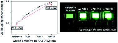
Due to the very low light extraction efficiency of conventional organic light-emitting diodes (OLEDs), the application of OLEDs for next-generation lighting remains limited. Therefore, in order to enhance the light extraction efficiencies that result in improving the luminous efficacy (LE, lm W−1) and external quantum efficiency (ηEQE, %) of OLEDs, three different geometrically profiled, negatively nanostructured periodic semi-pyramid polydimethylsiloxane (PDMS) layers are used to create a hole at depths of 500 nm, 650 nm, and 1000 nm; these are designated as the polymeric lighting extraction film (PLEF) I, PLEF II, and PLEF III, respectively. These layers are placed directly on the backside of the green emissive bottom-emitting OLED (BE-OLED) glass substrates as an outcoupling enhancement PLEF that improves the glass substrate/air interface. Through the simple combination with three different nanostructures on each green emissive BE-OLED, a maximum enhancement of up to 50% is achieved in the LE and ηEQE measured at the same brightness, which is 1.5 times higher than the reference green emissive BE-OLED without a PLEF. Therefore, global energy saving can be achieved through reducing the power consumption by up to 30% possibly estimated from LE using the integrated PLEFs.
Introduction
Recently, with significant concerns being raised about the global environment, energy saving issues in lighting applications have become a key strategy in conservation efforts.1–3 For energy saving requirements in lighting applications, light emitting diodes (LEDs) that generate light using inorganic semiconductors and organic light-emitting diodes (OLEDs) that generate light using organic semiconductors are the most favorable candidates for lighting options when compared with using filaments or gas. For LEDs, their lighting applications have prevailed in the global market and they have already been integrated into everyday life. However, LEDs remain economically inefficient due to their high process cost and they are also limited in shape flexibility because of its brittle structures. Moreover, LEDs are tiny light points, which mean that there are restrictions in large area lighting applications. However, OLEDs have been intensively investigated as next-generation energy-efficient lighting applications in order to attain environmental and financial benefits of more than %230 billion annually worldwide.1,4 Moreover, OLEDs have significant advantages such as high design flexibility, thin appearance, and light weight. Nevertheless, the OLED technology must be improved because typical OLEDs have a very low light extraction efficiency of only 20%, as a result of the different refractive indices among the substrate, anode, organic materials, and air.5–8 This non-continuous interface cause high internal reflection of the generated light (approximately 80%), which results in increased the power consumption. This is the primary obstacle to improve the light outcoupling efficiency of OLEDs.
In order to address this drawback, there have been significant efforts to increase the light outcoupling efficiency limits through introducing internal (as waveguide modes) and external (as substrate modes) interface modifications. However, by employing optical structures such as photonic crystals,9 random nanostructures,5 and/or low index grids4 to modify the waveguide modes at the interface between the organic layers and indium–titanium-oxide (ITO) anode, the effective improvement of outcoupling efficiency can be prevented using an appropriate stack design that will result in changes in the electrical behavior of the devices. Accordingly, extracting light in substrate modes has been considered as an alternative approach to enhance the light outcoupling efficiency. Previously, negatively nanostructured periodic semi-pyramid polydimethylsiloxane (PDMS) layers with three different geometrical profiles were fabricated using a simple but powerful imprinting-assisted replication process for a broadband anti-reflection effect.10 Here, in order to achieve a large enhancement of light extraction, it is important to explore all the physical parameters that modify the light propagation via diffraction on nanostructures of the OLED light source. Therefore, the enhancement of the light outcoupling efficiency is experimentally demonstrated through introducing three different geometrically profiled, negatively nanostructured periodic semi-pyramid PDMS layers. The three different replicated geometrical profiles are designated as the polymeric lighting extraction film (PLEF) I, PLEF II, and PLEF III. They are integrated directly on the backside of the green emissive bottom-emitting OLED (BE-OLED) glass substrates in order to investigate the influence of the three different replicated geometrical profiles with hole shapes at depths of 500 nm, 650 nm, and 1000 nm. In order to ensure that the proposed technique is promising as an energy saving approach, the light outcoupling enhancement is demonstrated in the luminous efficacy (LE) related to power consumption.
Experimental
Materials
96% sulfuric acid, 30% hydrogen peroxide, isopropyl alcohol (IPA), hexamethyldisilazane (HMDS), and trichloro(1H, 1H, 2H, 2H-perfluorooctyl)silane (FOTS, 96%) were purchased from Sigma-Aldrich (USA) and used without further purification. A positive photoresist (PR, SS03A9) based on phenol-formaldehyde resin and its developer (NMD-3) were provided by Dongwoo Fine Chem. Co., Ltd. (Korea) and Tokyo-Ohka (Japan), respectively. The thermally curable polydimethylsiloxane (PDMS), which is a mixture of Sylgard 184 and its curing agent (Dow Corning, USA), constitutes the functional group that undergoes extensive cross-linking via thermally-induced radical polymerization. All materials used for the green emissive BE-OLED fabrication were electronic grade and were used without further purification.
Fabrication of the green emissive bottom-emitting OLED (BE-OLED)
The structure of the BE-OLED was ITO (70 nm)/HATCN (10 nm)/1,1′bis-((4-methylphenyl)aminophenyl)cyclohexane (TAPC, 45 nm)/HATCN (5 nm)/TAPC (45 nm)/HATCN (5 nm)/TAPC (45 nm)/HATCN (5 nm)/TAPC (45 nm)/3 wt% fac-tris(2-phenyl-pyridine) iridium(III) (Ir(ppy)3)-doped 2,6-bis[3-(9H-carbazol-9-yl)phenyl]pyridine (DCzPPy, 20 nm)/1,3-bis(3,5-dipyrid-3-yl-phenyl)benzene (BmPyPB, 55 nm)/LiF (1 nm)/Al (100 nm). The emission layer emits a green color, with its main peak at λ = 510 nm. The active luminous area is 7 × 10 mm2. All organic layers were deposited in a high vacuum chamber below 5 × 10⁻⁷ Torr using a thermal evaporator. In order to avoid degrading the organics due to the moisture and oxygen in the air, the fabricated OLEDs were encapsulated in glass in a glove box.
Fabrication of the textured Si master
The process flows of the Si-master fabrication and imprint processes are illustrated in Fig. 1. A 6-inch Si wafer was cleaned in a piranha solution (a 3
:
1 mixture of 96% sulfuric acid and 30% hydrogen peroxide) at room temperature for 30 min, rinsed with deionized (DI) water and IPA to remove the organic and inorganic impurities from the Si-wafer surface, and dried using N2 gas (Fig. 1(a)). Then, the dried Si-wafer was spin coated with HMDS and baked at 90 °C for 90 s in order to improve the PR adhesion to the Si wafer surface (Fig. 1(b)). A commercially available PR (SS03A9) was spin coated at a rate of 4000 rpm for 30 s in order to obtain a thickness of approximately 1000 nm on the Si wafer, and the quadratic patterns were prepared using a conventional photolithography method with a stepper (NSR2205i1 1D, Nikon, Japan) (Fig. 1(c)). Subsequently, the Si wafer was placed on a wafer holder of the mask aligner with a UV light in an MA 6 tool (Suss Microtech, Germany), exposed to 365 nm light (intensity: 20 mW cm−2) for 40 s in a non-contact mode, and screened using a quartz mask with feature sizes ranging from 500 nm to 1500 nm. Then, it was post-exposure baked at 110 °C for 90 s in order to elevate the hardening process, developed in NMD-3 for 60 s, and hard baked at 120 °C for 90 s. Next, the photo-patterned Si-wafer was etched via deep reactive ion etch (DRIE) using SF6/O2 plasma. The remaining PR on the Si wafer was stripped using an O2 plasma treatment. Finally, the textured Si-masters with three different profiles with depths of 500 nm, 650 nm, and 1000 nm were obtained.
 |
| Fig. 1 A schematic of the overall processes flow for fabricating the textured Si-master using a conventional photolithography method. (a) A cleaned Si wafer is surface-treated using HMDS as an adhesion promoter. (b) A positive photoresist (PR, SS03A9) is spin coated on the HMDS treated Si wafer. (c) The PR layer is photo-patterned using a Stepper, UV-exposed with 20 mW cm−2 for 40 s, post-exposure baked at 110 °C for 90 s, developed in NMD-3 for 60 s, and hard baked at 120 °C for 90 s. (d) The photo-patterned Si wafer is etched via photomask using deep reactive ion etching (DRIE) process with SF6/O2 plasma. (e) The remaining PR on the Si wafer was stripped using an O2 plasma treatment and finally the textured Si-master was obtained with three different geometrical profiles at depths of 500 nm, 650 nm, and 1000 nm. | |
Fabrication of the external polymeric lighting extraction film (PLEF)
In order to fabricate the external PLEF using the textured Si master fabricated via conventional photolithography, a drop-casting method was implemented. The overall process flow for the patterning of the external PLEF is presented in Fig. 2. First, a PDMS prepolymer was prepared from Sylgard 184 by mixing with a ratio of ten parts of the base to one part of the curing agent. Before the PDMS prepolymer was used, it was placed in a vacuum desiccator for 30 min in order to remove the bubbles. Prior to the imprinting process, the textured Si-master was chemically treated with trichloro(1H, 1H, 2H, 2H-perfluoro-octyl)silane (FOTS) in order to form a hydrophobic self-assembled monolayer (SAM) for sufficient pattern transfer from the textured Si master onto the PDMS layer (Fig. 2(a) and (b)).11,12 Then, the PDMS prepolymer was drop-cast on the FOTS-treated textured Si master (Fig. 2(c)) and covered with the backside of the green emissive BE-OLED glass substrate (Fig. 2(d)) at a pressure of 1 kg in order to transfer the pattern effectively. Subsequently, they were cured at room temperature for 48 h in order to increase the cross-linking density and minimize the thermal damage in the organic layer. Finally, the textured Si master was removed from each cured external PLEF (Fig. 1(e)). The negative semi-pyramid nanostructures with three different geometrical profiles were transferred onto the backside of the green emissive BE-OLED glass substrates with high pattern fidelity (Fig. 2(e)).
 |
| Fig. 2 A schematic of the overall processes flow for fabricating the negative semi-pyramid nanostructured PLEF using an imprinting-assisted replication process. (a) A cleaned textured Si master fabricated using a conventional photolithography method is prepared. (b) The vaporized FOTS forms a self-assembled monolayer (SAM) on the surface of the textured Si master. (c) The PDMS prepolymer is dispensed onto the FOTS-treated textured Si master. (d) And then, it is covered with the backside of the green emissive BE-OLED glass substrate and is pressed with 1 kg of pressure for 48 h. (e) The PDMS layer is detached from the textured Si master, leaving negative semi-pyramid nanostructures with three different geometrical profiles at depths of 500 nm, 650 nm, and 1000 nm. | |
Characterization
A scanning electron microscopy (SEM) was performed in the secondary electron imaging mode at 10 keV using a high-resolution finite element SEM (FE-SEM, Sirion 400, USA). In order to measure the transmittance of the external PLEF, the transmittance of the external PLEF was obtained using a double-lamp light UV-VIS-NIR spectrophotometer (Hitachi U-3501, Japan) and this was compared with a non-patterned polymer layered glass as a reference. The open area of all prepared external PLEFs was 10 × 10 mm2. The current–voltage–luminance (I–V–L) characteristics were measured using a current–voltage source unit (Keithley 238, Keithley Instruments, Inc., USA). The angular-dependent brightness and electroluminescence (EL) spectra were measured using a goniometer-equipped spectroradiometer (Minolta CS-2000, Japan) at a constant current density level of 2 mA cm−2.
Results and discussion
A schematic of the green emissive BE-OLED structure and SEM images of negative semi-pyramid nanostructures as PLEFs fabricated using the Si masters are presented in Fig. 3. For the green emissive BE-OLED structure in Fig. 3(a), 3 wt% Ir(ppy)3 [fac-tris(2-phenylpyridine) iridium(III)]-doped DCzPPy [2,6-bis [3-(9H-carbazol-9-yl)phenyl]pyridine] was used as the emitting layer (EML) with ITO as the bottom electrode and LiF/Al as the top electrode. The TAPC [1,1′(bis-(4-methylphenyl)amino-phenyl)cyclohexane] alternately stacked with HATCN and BmPyPB [1,3-bis(3,5-dipyrid-3-yl-phenyl)-benzene] were used as the hole transporting layer (HTL) and electron transporting layer (ETL), respectively. For the PLEF used as the external light extraction layer for the green emissive BE-OLED, the scanning electron microscopy (SEM) images of the periodically textured Si masters with cross-sectional views are presented in Fig. 3(b) to (d); these figures indicate that the patterned periodic textures have tapered positive cone profiles with negative semi-pyramid shapes at depths of approximately 500 nm, 650 nm, and 1000 nm.10 Fig. 3(e) to (g) show SEM images of the PLEFs replicated from the Si masters using PDMS. The total area of the negative semi-pyramid nanostructured PLEF transferred patterns from the FOTS-treated periodically textured Si master using the UV-NIL technique was 10 × 10 mm2. The negative semi-pyramid nanostructures in the PLEF have approximately the same geometrical profiles as the periodically textured Si masters. As shown in Fig. 3(e) to (g), the notable differences of the negative semi-pyramid nanostructured PLEFs are the depth from the top surface of the open areas and the differently tapered shapes.
 |
| Fig. 3 (a) A schematic of the green emissive BE-OLED without (as a reference, left) and with (right) the negative semi-pyramid nanostructured PLEFs. (b) to (d) SEM images of the periodically textured Si masters with the different geometrical profiles at depths of (b) 500 nm, (c) 650 nm, and (d) 1000 nm. (e) to (g) Dedicated SEM images of the PLEF I, PLEF II, and PLEF III that are replicated from (b) to (d), respectively, using an imprinting-assisted replication processes.10 ((b) to (g): Images courtesy of RSC Advances). | |
In order to investigate the performance of PLEFs integrated directly on the green emissive BE-OLED for light outcoupling enhancement, the current density–voltage characteristics and electroluminescence (EL) spectra are characterized as shown in Fig. 4. In Fig. 4(a), the green emissive BE-OLED without the PLEF is demonstrated to have turned on at the same voltage of 3 V and it exhibited very low leakage current. The green emissive BE-OLED with PLEF III does not indicate electrical behavior changes as a result of externally integrated PLEF after the encapsulation process for the green emissive BE-OLED is completed. And it was found to be exhibited almost identical behavior as PLEF I and PLEF II. However, through employing the relatively simple method of improving the outcoupling efficiency, a remarkable tendency was observed in the EL spectra measured in the normal direction at 2 mA cm−2 as seen in Fig. 4(b). The integrated PLEF I, PLEF II, and PLEF III exhibited the different geometrical profiles that affect the EL intensities.
 |
| Fig. 4 (a) Current density–voltage characteristics of the green emissive BE-OLED without the PLEF (as a reference) and with the PLEF III (which exhibited almost identical behavior as PLEF I and II). (b) EL spectra of the green emissive BE-OLEDs measured in the normal direction at a current density of 2 mA cm−2. Inset: Magnified view of the increased EL spectra in the comparison with PLEF I, PLEF II, and PLEF III. | |
In order to evaluate the influence of the different geometrical profiles among the PLEF I, PLEF II, and PLEF III on the light extraction efficiencies, the angular dependences of the brightness and EL spectra were measured as shown in Fig. 5. In Fig. 5(a), the reference green emissive BE-OLED without the PLEF exhibited emission patterns that indicated a weak microcavity effect formed between the metallic cathode and ITO anode.13,14 This weak microcavity effect was demonstrated from its normalized EL spectra that exhibits a slight red-shift when the viewing angle increases (see Fig. 5(b), as a reference). However, this phenomenon could be shielded by integrating the PLEFs directly on the green emissive BE-OLED. Through integrating PLEF II and PLEF III, the brightness was largely enhanced in a wide range from 20° to 70°; in contrast, PLEF I presented an enhancement in over a short range from 10° to 40°, which could be caused by insufficient depth of 500 nm for the light rays crashing into the wall.15 Fig. 5(c) to (e) demonstrate the angular dependency of the normalized EL spectra for the green emissive BE-OLEDs with the PLEF I, PLEF II, and PLEF III, respectively.
 |
| Fig. 5 (a) Angular dependences of the brightness. (b) to (e) EL spectra of the green emissive BE-OLEDs without the PLEF (as a reference) and with the PLEF I, PLEF II, and PLEF III, respectively. | |
In order to correlate the luminous efficacy (LE, lm W−1) and external quantum efficiency (ηEQE, %) of the green emissive BE-OLEDs without the PLEF (as a reference) and with PLEF I, PLEF II, and PLEF III, LE and ηEQE were then calculated over an angle range of – 70° ∼ 70°, and were plotted as a function of brightness (cd m−2). As seen in Fig. 6(a), the LE value of the green emissive BE-OLED without the PLEF was 37.6 lm W−1 at brightness of 1000 cd m−2, while the LE value of the green emissive BE-OLEDs with the PLEF I, PLEF II, and PLEF III were greatly enhanced up to 55.0 lm W−1 at the same brightness of 1000 cd m−2. Moreover, the ηEQE value also increased from 16.0 % to 22.8 % for the green emissive BE-OLED without the PLEF and with the PLEF I, PLEF II, and PLEF III (see Fig. 6(b)). In general, the refractive index profile from the substrate to the air was gradually and continuously changed via the cone structures, which have a very sharp angle from the bottom to the top; this increased the number of light rays crashing into the wall. However, the replicated PLEFs fabricated using the UV-NIL technique had negative nanostructures creating a hole shape at depths of 500 nm, 650 nm, and 1000 nm in the PLEF I, PLEF II, and PLEF III, respectively. Through increasing the depth of the hole profiles, the light extraction efficiencies also increased because the number of light rays crashing into the wall also increased.15
 |
| Fig. 6 (a) Luminous efficacy (LE, lm W−1) and (b) external quantum efficiency (ηEQE, %) versus brightness (cd/m2) of the green emissive BE-OLEDs without the PLEF (as a reference) and with PLEF I, PLEF II, and PLEF III. At the same brightness of 1000 cd m−2, the LE and ηEQE were significantly enhanced up to approximately 50% through simply integrating the PLEFs directly on the green emissive BE-OLEDs. | |
The light extraction enhancement was demonstrated with the integration of PLEFs directly on the green emissive BE-OLED in order to reduce the optical barrier at the glass substrate/air interface. In Fig. 7(a), the light enhancement is plotted against the green emissive BE-OLEDs without and with the PLEFs measured at the brightness of 1000 cd m−2. The highest outcoupling enhancement of the green emissive BE-OLED was achieved with the integrated PLEF III that had the largest hole depth of 1000 nm; it was enhanced by 1.5 times. Moreover, the outcoupling enhancement measured at the same brightness of 1000 cd m−2 demonstrated using the integrated PLEFs is presented in Fig. 7(b). Therefore, this approach indicates energy saving in terms of the power consumption being reduced by approximately 30% possibly estimated from LE compared to the green emissive BE-OLED without a PLEFs.
 |
| Fig. 7 (a) Outcoupling enhancement measured at the brightness of 1000 cd m−2 as a function of the green emissive BE-OLED without the PLEF (as a reference) and with the PLEF I, PLEF II, and PLEF III. (b) Photographs of the lighting images of the green emissive BE-OLEDs without the PLEF (as a reference) and with the PLEF I, PLEF II, and PLEF III measured at the same voltage. The green emissive BE-OLEDs were significantly brighter than the reference BE-OLED without the PLEF. | |
Conclusions
A simple, fast, low-cost, yet powerful technique to fabricate polymeric lighting extraction film (PLEF) was introduced for light outcoupling enhancement. The light extraction efficiencies of the green emissive BE-OLEDs were demonstrated using replicated nanostructures in the PDMS layer with three different hole depths. In the results, the luminous efficacy (LE, lm W−1) and external quantum efficiency (ηEQE, %) measured at the same brightness of 1000 cd m−2 were significantly enhanced by 50% through the integration of the PLEF I, PLEF II, and PLEF III directly on the green emissive BE-OLEDs. Moreover, this approach is promising for sufficient energy efficiency, which results from the energy saving in terms of the power consumption being reduced by 30%, compared with the reference green emissive BE-OLED without PLEFs.
Acknowledgements
This work was supported by the IT R&D program of MSIP/KEIT (Grant no. 10041416, the core technology development of light and space adaptable new mode display for energy saving on 7 inch and 2 W).
Notes and references
- Y. Takei, Environment and Energy Research Unit, QUARTERLY REVIEW, 2009, vol. 32, pp. 59–71 Search PubMed.
- C. C. M. Kyba, A. Hänel and F. Hölker, Energy Environ. Sci., 2014, 7, 1806–1809 Search PubMed.
- International Energy Agency, Lights labour's lost: policies for energy-efficient lighting, OECD/IEA, Paris, 2006 Search PubMed.
- Y. Sun and S. R. Forrest, Nat. Photonics, 2008, 2, 483–487 CrossRef CAS.
- J.-W. Shin, D.-H. Cho, J. N. Moon, C. W. Joo, S. K. Park, J. Lee, J.-H. Han, N. S. Cho, J. Hwang, J. W. Huh, H. Y. Chu and J.-I. Lee, Org. Electron., 2014, 15, 196–202 CrossRef CAS PubMed.
- P. A. Hobson, S. Wedge, J. A. E. Wasey, I. Sage and W. L. Barnes, Adv. Mater., 2002, 14, 1393–1396 CrossRef CAS.
- H. Greiner, Jpn. J. Appl. Phys., 2007, 46, 4125 CrossRef CAS.
- H. Benisty, H. de Neve and C. Weisbuch, IEEE J. Quantum Electron., 1998, 34, 1612–1631 CrossRef CAS.
- K. Saxena, V. K. Jain and D. S. Mehta, Opt. Mater., 2009, 32, 221–233 CrossRef CAS PubMed.
- J.-C. Woo, N. S. Baek, J. Y. Kim and C.-I. Kim, RSC Adv., 2012, 2, 7677–7680 RSC.
- J. Y. Kim, K.-S. Park, Z.-S. Kim, K.-H. Baek and L.-M. Do, Soft Matter, 2012, 8, 1184–1189 RSC.
- J. Y. Kim, D.-G. Choi, J.-H. Jeong and E.-S. Lee, Appl. Surf. Sci., 2008, 254, 4793–4796 CrossRef CAS PubMed.
- J. Lee, N. Chopra and F. So, Appl. Phys. Lett., 2008, 92, 033303 CrossRef PubMed.
- V. Bulović, V. B. Khalfin, G. Gu, P. E. Burrows, D. Z. Garbuzov and S. R. Forrest, Phys. Rev. B: Condens. Matter Mater. Phys., 1998, 58, 3730–3740 CrossRef.
- S. Tanaka, Y. Kawakami and Y. Naito, Proceedings of SPIE 49th annual meeting, 2004, vol. 5519–33, pp. 184–193 Search PubMed.
|
This journal is © The Royal Society of Chemistry 2015 |
Click here to see how this site uses Cookies. View our privacy policy here.