
Electric field effect dominated bipolar resistive switching through interface control in a Pt/TiO2/TiN structure†
Dong-Hyeok Lima,
Ga-Yeon Kima,
Jin-Ho Songa,
Kwang-Sik Jeonga,
Dong-Chan Kimb,
Seok-Woo Namb,
Mann-Ho Cho*a and
Tae-Geol Leec
aInstitute of Physics and Applied Physics, Yonsei University, Seoul 120-749, Korea. E-mail: mh.cho@yonsei.ac.kr
bProcess Development Team, Semiconductor R&D Division, Samsung, Suwon 445-701, Korea
cKorea Research Institute of Standards and Science, Daejeon 305-340, Korea
First published on 24th November 2014
Abstract
To investigate the reproducibility and I–V non-linearity characteristics in resistive-switching random-access memory (RRAM), we studied the switching characteristics through Pt/TiO2 interface control using a non-stoichiometric TiO2−x/TiN interface formation in a resistive switching Pt/TiO2/TiN stack. Using the TiO2−x/TiN interface instead of the TiO2/TiN interface induced nearly forming-free switching, decreased the reset current, suppressed the gradual reset process, and resulted in faster switching by electric pulse. These results indicate that the Pt/TiO2 interface experienced reduced oxygen-vacancy-mediated switching. The discrepancy between the reduced oxygen-vacancy-mediated switching and the initially large number of oxygen vacancies can be resolved via the oxygen vacancy distribution dependent field effect. To clarify this process, we performed reaction-diffusion-drift model simulations. The drift velocity, which was calculated using the vacancy distribution, described the dynamic movement, and the simulation results supported the experimentally observed faster switching response. The field effect, which provided successive feedback between the drift velocity and vacancy distribution, can potentially be exploited to generate vacancy-designed devices.
I. Introduction
The switching mechanisms of RRAM have been intensively explored and proposed.1–11 Besides ionic-motion-based models,12,13 electronic-,13,14 magnetic-,15 ferroelectric-,16 and microstructural change-based17 resistive switching phenomena are examined. Among the several kinds of resistive switching materials,2,8,18,19 such as oxides, chalcogenides, and nitrides, titanium dioxide is frequently and widely investigated as a standard material due to its variety of functionalities, including unipolar resistive switching (URS),20,21 bipolar resistive switching (BRS),22,23 complementary resistive switching24,25 (CRS), programmable metallization cell26,27 (PMC) as an electrolyte, and spike timing dependent plasticity28,29 (STDP).Meanwhile, various layered-oxide systems recently show better device performance,30,31 and experimental results in TiO2/TiO2−x systems3,5,25,32–34 reveal the importance of oxygen-deficient-layer TiO2−x related with forming-free operation and sufficiently large numbers of oxygen vacancy sources. In these systems, the switching mechanism is understood as anionic motion of the oxygen ion (equivalently, positive charged oxygen vacancy) when an electrochemically inert metal electrode such as Pt is used.22,35–38 The forming-free operation in the TiO2/TiO2−x system can be achieved by fabricating an initially off-state device,5 where the initial resistance is controlled by thickness of TiO2−x layer. Compared with a single TiO2 system under low current compliance, which shows CRS under limited oxygen vacancy conditions due to the low current compliance,25,39,40 the TiO2/TiO2−x system shows similar behavior to the single TiO2−x system with sufficient oxygen vacancy sources. Moreover, the oxygen vacancy content can be controlled by the current compliance during electroforming.25 Although achieving forming-free operation in the oxygen-deficient layer inserted system implies the possibility of consistent on/off states due to the absence of irreversible breakdown processes,5 the sufficiently large number of oxygen vacancies cannot directly explain the device performance improvement.
Interestingly, our electrical measurement results commonly indicate fewer residual oxygen vacancies at the Pt/TiO2 interface in the Pt/TiO2/TiO2−x/TiN structure during switching, compared with those at the Pt/TiO2 interface in the Pt/TiO2/TiN structure. Furthermore, nearly forming-free switching, which initially exhibits a nearly off-state (non-typical on-state) without the initial-to-off state transition, in the Pt/TiO2/TiO2−x/TiN structure implies less oxygen vacancy generation near the Pt/TiO2 interface. However, the large number of oxygen vacancies can possibly be involved in generating a stronger conduction path due to the initially abundant oxygen vacancy sources of TiO2−x. Thus, the discrepancy between few residual vacancies at the Pt/TiO2 interface and the initially sufficient oxygen vacancy sources should be resolved.
Although the physical origin of the filamentary conduction path has been determined to some extent, formation and de-formation of the path are extremely complex. For example, oxygen vacancies (equivalently, oxygen ions) play an important role in resistive switching in various anionic oxide systems,41–44 but the set and reset operations can be achieved in various ways. In anionic motion-based switching, the field effect is antipodal with the thermal effect due to the unique properties of the electric field effect.8 The field-dominating memory effect is bipolar, low power consuming, and has non-linear I–V characteristics, while the thermal-dominating memory effect is unipolar, high power consuming, and has linear I–V characteristics. However, because the electric field and thermal effects are simultaneously involved in resistive switching, they are difficult to separate. The field effect is largely preferred because of its low power consumption and non-linear I–V characteristics, which are essential for high-density crossbar array architectures. Ionic movement induced by the electric field effect is thought to be a primary factor governing the switching process in BRS systems, indicating that the dependence of switching characteristics on the electric field effect should be analyzed.
In this study, we investigate the I–V characteristics of films with an oxygen-vacancy-abundant layer inserted in the Pt/TiO2/TiO2−x/TiN structure. The difference in behavior observed due to the presence of a high concentration of oxygen vacancies, such as fewer residual oxygen vacancies at the Pt/TiO2 interface during switching, the consequent fast switching response, and an improvement in I–V non-linearity, clearly showed the significance of the electric field effect. We also discuss the switching process in terms of the oxygen vacancy distribution dependent field effect and qualitatively examine the possibility of oxygen vacancy-designed devices using a reaction-diffusion-drift model simulation. Although several TiOx-based papers have been reported with TiOx acting as a prototypical oxide for resistive switching, topics related to the formation and evolution of the non-stoichiometric region in the oxide have not yet been completely investigated. This is the reason why there are still many reports of studies related to this topic. For example, Yoon et al. recently reported on the evolution of the shape of the conducting channel in Pt/TiO2/TiO2−x/Pt.25 I. Salaoru et al. studied the origin of off-state variability based on the non-uniform displacement of ionic species, which contributes to the formation of conductive filaments in TiO2.45 M. Noman et al. reported on the mechanism of localized electrical conduction at the onset of electroforming in TiO2 based resistive switching devices.46 In this study, we focus on the role of the oxygen deficient layer in the forming behavior, evolution of the conduction path, and stability of resistance state.
II. Results and discussion
To investigate the effect of modifying the concentration of oxygen vacancies in detail, we prepared a sample with oxygen vacancies controlled in the depth direction. In the sample, the oxygen content of TiO2−x was increased stepwise from the bottom TiN electrode to the top Pt electrode, resulting in a high concentration of oxygen vacancies near the TiN electrode and stoichiometric TiO2 beneath the Pt electrode. The preparation and confirmation of the fabricated samples are discussed separately in the methods section and in the ESI.† We denote the resulting device structure as Pt/TiO2/TiO2→2−x/TiN (or simply Pt/TiO2/TiO2−x/TiN), where the subscript 2 → 2 − x indicates the decreasing amount of oxygen (or increasing amount of oxygen vacancies). Schematic diagrams of the prepared samples are depicted in Fig. 1(a) for the reference Pt/TiO2/TiN sample and in Fig. 1(b) for the Pt/TiO2/TiO2−x/TiN sample. In the figures, the interfaces are denoted as a large Schottky diode, small Schottky diode, and a resistor. The large Schottky diode indicates the rectifying Pt/TiO2 interface3,47–49 in both samples. The small Schottky diode and the resistor indicate the TiO2/TiN and TiO2−x/TiN interfaces, respectively.50 Rectification of the Pt/TiO2 interface is reflected in the low voltage I–V characteristics shown in Fig. 1(c). The low current at a negative voltage for both samples is due to Schottky barrier formation, which prohibits electrons crossing the interface from Pt to TiO2.51 For Pt/TiO2/TiN, the slightly higher current at a positive voltage than that at a negative voltage is due to relatively weak barrier formation at the TiO2/TiN interface than that at the Pt/TiO2 interface. Moreover, the very high current at a positive voltage for Pt/TiO2/TiO2−x/TiN is due to the absence of a barrier at the TiO2−x/TiN interface.50 Under a low voltage sweep (−1 V to +1 V), which did not induce switching, the interface characteristics of the pristine states were clearly distinguishable. | ||
| Fig. 1 Schematic diagrams of the prepared samples of (a) Pt/TiO2/TiN and (b) Pt/TiO2/TiO2−x/TiN. (c) Comparison between the pristine I–V characteristics of (a) and (b). | ||
Generally, resistive switching devices require initiation of the device, which is referred to as electroforming (or simply forming).5,52 Although a symmetric device structure, such as Pt/TiO2/Pt that possibly exhibits corresponding (ideally and experimentally) symmetric pristine I–V characteristics,37 can be identically electroformed regardless of the voltage polarity, an asymmetric device structure due to different metal electrodes, such as Pt/TiO2/TiN that exhibits corresponding intrinsically asymmetric pristine I–V characteristics,53 can be electroformed differently with respect to the sequence of voltage application. The forming-on process sets the initial state to the on-state, as shown in Fig. 2(a), while the forming-off process sets the initial state to the off-state, as shown in Fig. 2(b). The following operation is the switching-off (reset) in the forming-on process and the switching-on (set) in the forming-off process. The forming-off process contrasts markedly with forming-on process in that the Schottky-like interface (Pt/TiO2), which is the most important switching region in this asymmetric metal (Schottky-like)/TiO2/metal (ohmic-like) structure, is less deformed.5 For this reason, we used the forming-off process to investigate the Pt/TiO2 interface. For an initially high pristine current device such as Pt/TiO2/TiO2−x/TiN, the forming-off process could show the switching behavior shown in Fig. 2(c). Although the switching sequence is as same as that shown in Fig. 2(b), the current of the forming-off process is very high, as shown in Fig. 3(c). The current level is higher than the possible switching-on (set) current compliance, but the device is still in the off-state. In this high current forming-off device, the off-state is close to the initial state, so the forming-off process could not induce a remarkable change in current. In this way, a forming-free switching sequence is possible. This implies that the set process (rather than the electroforming) can cause significant changes, such as Coulomb attraction of the oxygen vacancy from the TiO2−x electrode to the Pt electrode according to the anionic motion-based switching mechanism, in the Pt/TiO2 interface region in Pt/TiO2/TiO2−x/TiN.
 | ||
| Fig. 2 Categorization of the electroforming process and concomitant switching sequence. (a) Forming-on process: initial-on–off–on sequence, (b) forming-off process: initial-off–on–off sequence, and (c) forming-off process: initial-off (≈initial)-on–off sequence. | ||
 | ||
| Fig. 3 The forming-off process for electroforming and the concomitant forming-on, forming-off process are sequentially demonstrated and explained for (a) Pt/TiO2/TiN and (b) Pt/TiO2/TiO2−x/TiN. | ||
Sequential operations for the forming-off, switching-on, and switching-off processes are shown for Pt/TiO2/TiN and Pt/TiO2/TiO2−x/TiN in Fig. 3(a) and (b), respectively. Even though the first positive voltage with a different current compliance can also be a forming-off process in that the next negative voltage sweep with sufficiently high voltage and current compliance possibly induces the on-state, we defined forming-off as a sufficiently high positive voltage (such as +10 V) with adequate current compliance that induced switching-on within −2 V with a 10 mA set current compliance during the next voltage sweep. In other words, we wanted to compare the difference between the initially almost off-state of Pt/TiO2/TiO2−x/TiN and the off-state of Pt/TiO2/TiN formed after the forming-off process with analogous set operations by comparing Pt/TiO2/Pt and Pt/TiO2/TiO2−x/Pt.5 Considering the current compliance during the forming-off process, the significantly higher current in Pt/TiO2/TiO2−x/TiN indicated the presence of more oxygen vacancies than necessary for a set operation. Moreover, due to the hard breakdown, the infeasibility of the forming-off process in Pt/TiO2/TiN using the same high current compliance required for Pt/TiO2/TiO2−x/TiN indicates not only quantitative but also qualitative differences in the oxygen vacancy distribution between Pt/TiO2/TiN and Pt/TiO2/TiO2−x/TiN. Thus, the comparison can be rationalized by the switching scheme, which considers the initial difference in the oxygen vacancy distribution as different requirements for the same set operation.
In our reference sample of Pt/TiO2/TiN, the forming-off current compliance at which the set process can be triggered varies over a wide range (50 μA to 1 mA) due to the random nature of the initial device state (data not shown). However, the forming-off current compliance is smaller than the typical set current compliance (10 mA). The switching sequence and conditions were as follows: low-voltage sweeping from 0 V to +1 V to read the initial current before the switching operation, positive forming-off with a compliance current of 50 μA, negative bias up to −2 V with a compliance current of 10 mA, and then positive bias up to +2 V without current compliance as shown in Fig. 3(a). The switching curves in Fig. 3(a) are similar to those shown in Fig. 2(b).
The Pt/TiO2/TiO2−x/TiN devices underwent a voltage-sweeping scheme similar to that applied to the reference Pt/TiO2/TiN devices, except for the forming-off current compliance. The initial current level was over 50 μA, and the forming-off current compliance for the Pt/TiO2/TiN sample at +1 V is shown (blue highlighted line #1) in Fig. 3(b). At the 0.5 mA sweep (#2), no significant changes were observed, such as the slight current decrease typically generated during the electroforming process. Even when the current compliance was increased up to a 10 mA sweep (#3), no significant changes were observed. The next sweep (#4) exhibited a counter-clockwise loop. To confirm the consistency of the loop, the sweep (#5) was repeated. The counterclockwise loop was unchanged (#6–#9) until the forming-off current compliance was over 10 mA, which implies that no significant changes occurred even in the high current of 10 mA. When the forming-off current compliance was 30 mA, the first set was observed within −2 V. At that time, the same set current compliance of 10 mA was applied during the set process. We compared the fabricated samples under this scheme with a reduced deforming forming-off process and the same set conditions.
To compare switching behaviors, a number of I–V curves were generated (see Fig. 4). In this figure, the first set and reset curves are distinguished from the following set and reset curves. We observed a clear difference in the current-decreasing features of the reset process between samples. The reset process in the vacancy-abundant sample became sharp without an additional gradual process (see circled areas in Fig. 4(a) and (b)). Although the memory window changed after the first set and reset, the difference in the sharpness of the reset remained consistent; gradual changes were observed in the Pt/TiO2/TiN film, whereas no gradual changes were observed for the Pt/TiO2/TiO2−x/TiN film. This result can be explained by the high current forming-off process depicted in Fig. 2(c) (red vertical arrow and symbol ‘x’). In contrast, Fig. 2(c) and 4(b) commonly show suppression of the additional gradual processes due to the high current off-state at a positive voltage. Strikingly, the maximum reset current (IReset) changed from a value over the set current compliance (ICompliance) to a value below the set current compliance after insertion of the oxygen-vacancy-abundant layer. Comparable IReset and ICompliance values indicate that the switching was mostly driven by the electric field over the narrow filament ruptured region,20 which likely exists in the Pt/TiO2 interface region of Pt/TiO2/TiO2−x/TiN. Thus, some of the oxygen vacancies could participate the switching, while other vacancies could act like a virtual electrode to enhance the electric field effect at the top electrode region. Furthermore, although the strengthened conduction path and high current requiring (Joule heat dominating) reset process are expected at the Pt/TiO2 interface due to the large amount of oxygen vacancies in Pt/TiO2/TiO2−x/TiN, the actual IReset value, which is compatible with or even less than the ICompliance value, reveals the narrow conduction path and possibly lower oxygen vacancy participation.39 The combination of this enhanced field effect and lower oxygen vacancies participation should mediate faster switching and non-linearity improvements due to the rectifying Pt/TiO2 interface after reset with fewer oxygen vacancies.
 | ||
| Fig. 4 A number of I–V curves are linearly displayed for (a) Pt/TiO2/TiN and (b) Pt/TiO2/TiO2−x/TiN. The first set and reset are distinguished from the subsequent set and reset curves. The differences in the current-decreasing feature and maximum reset current of the reset process are indicated. | ||
To evaluate whether there was an improvement in switching speed, switching behaviors were examined using electric pulses of various widths. This operation is similar to a voltage sweep: a positive pulse was used for forming, a negative pulse was used for the set, and a positive pulse was used for the reset. Additionally, the width of the positive pulse for the reset was decreased, while the width of the negative pulse for the set was left unchanged. In pulse-induced switching, forming-off, which originates from a stronger Coulomb repulsion rather than the oxygen vacancy supply at the Pt/TiO2 interface, did not occur. In other words, weak Coulomb repulsion due to the narrow pulse width did not form an off-state. Thus, the first positive pulse with a high voltage and narrow width induced a state of resistance (typically around 200 Ω for all the samples) in our devices although the initial resistance varied from 5 × 10⁴–5 × 10⁶ Ω. This could be an on-state in that the 2 V and 10 mA set voltage sweep implies a resistance of 200 Ω. Because the pulsed forming process exhibits a field effect (rather than a thermal effect) during the short time interval, pulse-width-dependent resistance changing behavior can show the difference in the agility of oxygen vacancy movement induced by the electric field effect enhancement.
The forming process (#1*) could generally be induced by a high narrow pulse (+10 V and 50 ns) in Pt/TiO2/TiN, as shown in Fig. 5(a). This forming process typically requires a single pulse or a few pulses. Then, to induce an off-state, a +2.5 V intentionally long (8 s) pulse was applied. The resistance increased by about one order of magnitude. This type of pulse was adequately high and wide compared with the voltage sweep reset of 0 to +2 V for a few seconds. The increased resistance decreased back to the on-state level after applying a single 50 ns pulse of −5 V.
 | ||
| Fig. 5 Recovery of the reset state is examined by electric pulse. During the reset, the reset state is well recovered for the pulse widths of up to 10 μs in (a) Pt/TiO2/TiO2−x/TiN while the reset state is not well recovered by applying repeated 8 s-width pulses in (b) Pt/TiO2/TiN. | ||
The repeated switching continued as the reset pulse width decreased. The numbered regions are divided by different pulse conditions, and the relative height and width of the pulses are depicted at the bottom of Fig. 5(a) and (b). In particular, in region 5, the resistance window gradually narrowed as the width of the pulse decreased from 1 s to 1 μs. The immediate increase in the reset pulse width to 10 μs (#6) could not maintain the stable on- and off-states. A similar operation was performed for Pt/TiO2/TiO2−x/TiN, as shown in Fig. 5(b). The forming process was triggered by a single 50 ns pulse or a few 50 ns pulses of +10 V, leading to an on-state of about 200 Ω. Although the number of pulses required to induce electroforming differed according to the initial conditions, even for the same Pt/TiO2/TiO2−x/TiN sample, the difference between Pt/TiO2/TiN and Pt/TiO2/TiO2−x/TiN in terms of resistance recovery behavior from a similar low resistance (about 200 Ω) in the on-state after forming can explain the differences in the reset process between these two film types. We attempted to form the on-state using a 10 V pulse with narrow widths of 100 ns, 200 ns, and 300 ns, but there was no significant change. Rather, a −5 V and 50 ns pulse formed the on-state, which is similar to the nearly forming-free voltage sweep behavior. Consistently, a +2.5 V, 8 s pulse was used to turn the oxygen-vacancy-abundant device to the off-state and significantly increased its resistance (over 104 Ω) over that of the reference device. For direct comparison, we applied a single −5 V and 50 ns pulse to set the device to the on-state and then applied a single +2.5 V pulse with various widths to reset the device to the off-state. The resistance states were slightly unstable, but the set/reset window was relatively wide. This on- and off-state switching continued until a 1 μs pulse width. However, the resistance of the off-state decreased immediately when the pulse width was reduced to 1 μs. Considering that the electric field-driven ionic motion is the driving force behind the reset process and that the thermal effect significantly or slightly (according to some conditions such as the operation current level) affects the switching behavior, +2.5 V is too low to induce sufficient field and/or Joule-heat effects for Pt/TiO2/TiN, even though it is sufficient to induce Coulomb repulsion for Pt/TiO2/TiO2−x/TiN. The requirement of a relatively low, sufficiently wide pulse for a high resistance state indicates drift of the oxygen vacancies rather than a thermal effect. This argument is supported by subsequent resistance changing behaviors in response to another pulse. Interestingly, an immediate resistance increase was observed when the pulse width was changed back to 10 μs in Pt/TiO2/TiO2−x/TiN, as shown in Fig. 6(a). Alternating set (−5 V and 50 ns) and reset (+2.5 V and 10 μs) pulses resulted in stable set/reset states. In contrast, the reset resistance in Pt/TiO2/TiN was improved by applying positive high narrow pulses (+10 V and 100 ns) for reset, as shown in Fig. 6(b). The reset resistance increased slowly after applying the high narrow pulses, even under the same alternating switching conditions (−5 V and 50 ns for set, +2.5 V and 10 μs for reset). The high voltage requirement for an increase in reset resistance suggested the presence of a large number of oxygen vacancies, which requires a stronger electric field or Joule heat effect for reset, at the Pt/TiO2 interface before application of the high voltage pulse. The high current requirement for the voltage sweep reset and the high voltage requirement for the voltage pulse reset imply that more oxygen vacancies are involved in switching in Pt/TiO2/TiN.
 | ||
| Fig. 6 Resistance changing behavior according to the pulse conditions. The number of pulses are counted immediately after each result in Fig. 5. (a) An immediate resistance increase was observed by applying a 10 μs pulse, and the set/reset states are stable in Pt/TiO2/TiO2−x/TiN. (b) The reset resistance was improved by applying positive, high, narrow pulses for reset in Pt/TiO2/TiN (region #6). | ||
Because the number of oxygen vacancies at the Pt/TiO2 interface is related to the change in the rectifying character of the interface, the quantitative change in the oxygen vacancies at the interface can be obtained from I–V behaviors. Therefore, the I–V non-linearity of the on-state and off-state were examined. In Fig. 7, guide lines (black solid) indicate ohmic-like contacts (log(I) is linearly proportional to log(V)); the positive and negative voltage regions were combined and both axes were logarithmically scaled. All data were normalized with respect to the non-zero lowest current value of the on-state. The Pt/TiO2/TiN sample showed characteristic behavior, i.e., linearity was observed (black arrows) in the low voltage region of both the on- and off-states, while non-linearity appeared (single black arrow) in the high voltage region of both the on- and off-states (Fig. 7(a)). The Pt/TiO2/TiO2−x/TiN sample showed different behavior; linearity was maintained (black arrows) even in the high voltage region in the on-state, while non-linearity appeared early (low voltage deviation from the single black arrow) in the low voltage region of the off-state (Fig. 7(b)). In the inset of Fig. 7, the current levels of the first set and reset at 0.01 V differed between the Pt/TiO2/TiN and Pt/TiO2/TiO2−x/TiN samples. The current level of Pt/TiO2/TiN was consistent before and after the reset process (purple circle), while that of Pt/TiO2/TiO2−x/TiN was not (separate red and blue circles indicate the off-state at negative and positive voltages, respectively). Because of the rectifying character of the Schottky-like barrier, the absence of residual oxygen vacancies near the Pt electrode can result in rectifying I–V characteristics. Thus, the inconsistent current level in the Pt/TiO2/TiO2−x/TiN case can be understood as limited oxygen vacancy generation; this initial presence of fewer oxygen vacancies at the Pt/TiO2 interface affected the non-linearity in the off-state current.
 | ||
| Fig. 7 The I–V non-linearity of each on-state and off-state is examined with reference to a guide line (black solid) indicating an ohmic-like contact. The positive and negative voltage regions are combined, and both axes are logarithmic scaled. Moreover, all data are normalized with respect to the non-zero lowest current value of the on-state. (a) The Pt/TiO2/TiN system shows characteristic behavior such that linearity is observed in the low voltage region of both the on- and off-state, and non-linearity is enhanced in the high voltage region of both the on- and off-state (black arrows). (b) The Pt/TiO2/TiO2−x/TiN system shows a contrast characteristic behavior such that linearity is enhanced even in high voltage region of the on-state, and non-linearity is enhanced early in low voltage region of the off-state. (Inset) the current level of the first set and reset at 0.01 V showed a clear difference between the Pt/TiO2/TiN and Pt/TiO2/TiO2−x/TiN samples. The current level was consistent before and after the reset process (purple circle) in Pt/TiO2/TiN, but it was not consistent (separate red and blue circles indicating the off-state in negative and in positive voltage, respectively) in Pt/TiO2/TiO2−x/TiN. | ||
The expected voltage-sweep switching processes are compared in Fig. 8(a) and (b). The first column indicates the initial differences in the oxygen vacancy distribution: no initial vacancies compared to a continuous increase in oxygen vacancies from inside the oxide to the bottom TiN electrode. The second column depicts the forming process, showing different oxygen vacancy supplies, Coulomb repulsion, and consequently residual oxygen vacancies. After the forming process, the concentration of oxygen vacancies near the Pt electrode in Pt/TiO2/TiN is expected to be higher than that in Pt/TiO2/TiO2−x/TiN due to large oxygen vacancy supply and/or insufficient Coulomb repulsion, indicated by the difference in their rectifying behavior, as shown in the inset of Fig. 7. Each state is expected to be similar to the off-state due to the forming-off scheme. The third column describes the set process resulting from the effects of Coulomb attraction, i.e., vacancies are attracted to the Pt electrode. Although the first set and reset show different behaviors in each case, the set processes can be described as repeated behaviors, except for the one-shot first set and reset processes. At this time, the vacancy concentration near the Pt electrode is expected to be higher in Pt/TiO2/TiN than in Pt/TiO2/TiO2−x/TiN after the set process due to the high current requirement of the voltage-sweep reset. The fourth column explains the reset process, which can be conversely thought of as Coulomb repulsion. Because the concentration of vacancies is low near the Pt electrode in Pt/TiO2/TiO2−x/TiN, the electrostatic force is sufficient to repulse the vacancies in a short amount of time, leaving no (or sufficiently fewer) residual vacancies near the Pt side. In contrast, in Pt/TiO2/TiN, residual vacancies can remain near the Pt side due to the high vacancy concentration. In this case, it takes significantly more time to repulse the vacancies. Thus, an additional gradual decrease in current is observed during repulsion at the Pt/TiO2 interface (black circle in Fig. 4(a)).
 | ||
| Fig. 8 Schematic diagram of the possible states (initial, forming, set, and reset) of resistive switching process for the (a) TiO2/TiN and (b) TiO2→2−x/TiN cases. Considering the combined interface effects, the strong or weak Schottky contact and high or low resistive ohmic contact are remarkable. The TiO2/TiN case has no initial vacancy, large oxygen vacancy supply, attraction with excessive vacancy participation, and repulsion with residual vacancy, while TiO2→2−x/TiN case has initial vacancy, small oxygen vacancy supply, attraction with low vacancy participation, and repulsion without residual vacancy. The amount of vacancy participation could be the origin of the different rectifying characters. | ||
To investigate the behavior of oxygen vacancies in detail according to the localized oxygen vacancy distribution, we qualitatively examined oxygen vacancy behavior using the reaction-diffusion-drift equation-based model simulation. The equation describes oxygen vacancy behavior as a combination of three different processes: generation,5 physical diffusion,54 and electric field-driven movement55 of oxygen vacancies (or equivalently oxygen ions). The originality of this simulation, distinguished from other similar model simulations,38,44,56,57 comes from incorporating the reaction terms such as vacancy generation during forming, and from the treatment of the drift term as not only vertical but also horizontal movement. Meanwhile, physical diffusion, which is induced by a gradient of concentrations, was considered, except for thermal migration. Although the thermal effects should be investigated, the field-enhanced effect due to the oxygen vacancy distribution has not been investigated prior to this study.
To simulate the resistive switching process, we added conditions to the original reaction-diffusion-drift simulation. The general results of the simulations are explained in the ESI.† When simulating the Pt/TiO2/TiO2−x/TiN case, a high oxygen vacancy concentration was configured as the initial condition. Similar to what we fabricated experimentally, the oxygen vacant regions formed a stepped structure, although the linearly configured vacancy condition produced a similar simulation result (data not shown). Although the results of XPS and TEM measurements (ESI†) were not able to show the stepped structure, the initial difference in oxygen content can be distinguished. Thus, the different oxygen vacancy distribution is significantly effective for the switching behavior in experiment and simulation. Fig. 9(a) shows a side-view of the initial vacancy concentration for Pt/TiO2/TiN and Pt/TiO2/TiO2−x/TiN. Although the reaction rate had the same values in both cases, fast vertical movement was observed in the Pt/TiO2−x/TiN case. This movement can be explained by the virtual electrode effect of the oxygen-deficient region (TiO2−x),58 which caused a steep potential gradient near the top electrode. The simulation was stopped when the minimum concentration of the central path exceeded the threshold concentration38 (green dotted line) as the final condition in Fig. 9(b). This simulation process mimics the electroforming process. In the forming process, each horizontal center (a point in the vertical center line), which maintains the horizontal maximum concentration, is vertically interconnected (filamentary conduction path). The vacancy concentration was lower beneath the top electrode in the Pt/TiO2/TiO2−x/TiN case than in the Pt/TiO2/TiN case. Furthermore, the location of the vertical minimum region (indicated by red circles) far from the top electrode in the Pt/TiO2/TiN case indicated that, in the simulation, a longer time was required to satisfy the threshold condition compared to the Pt/TiO2/TiO2−x/TiN case. Before the cycle test, forming-off states were obtained by allowing the voltage bias to remain for some time after satisfying the threshold condition without reaction, which is known as the overshooting phenomena in voltage-driven switching.58 Then, the set and reset operations were treated as repetitions of the diffusion-drift process with respect to the alternating sign of the voltage, and 20 cycles of switching were performed. The set process was treated as exceeding the threshold concentration at the top interface where the least number of vacancies are located. For consistent simulations, the applied voltage was maintained for the same period of time (voltage-applying time without reaction during forming) after the vacancy concentrations exceeded the threshold concentration at the top interface. Similarly, the applied voltage was maintained for the same period of time after the vacancy concentrations decreased below the threshold concentration at the top interface during the reset process. The results after 20 cycles of set and reset are shown in Fig. 9(c). A low concentration of vacancies was maintained near the Pt/TiO2 interface in the Pt/TiO2/TiO2−x/TiN case. Fig. 9(d) shows the vacancy distribution after 20 set/reset cycles. This simulation, based on reaction-diffusion-drift, described how the concentration of oxygen vacancies changed. The oxygen vacancy concentration remained low, especially in the region beneath the top electrode, in the Pt/TiO2/TiO2−x/TiN case. As a result, the simulation provides possible field-enhanced oxygen vacancy movement exhibiting lower oxygen vacancy participation. Although the residual oxygen vacancy was not observed in this simulation, the residual vacancy effect can originate from the thermal effect. Because the reported residual vacancy effect was simulated on the assumption of cylinder-like filamentary conduction path for the only reset process, a combination of the field effect (governing the forming and the set process as well as the reset in this simulation) and the reported thermal effect needs to be investigated.56
 | ||
| Fig. 9 Simulation results according to the experimental situation for different initial conditions. (a) Shortly after the simulation starts, the results show fast downward movement with considerable vacancy concentration as the initial condition from the bottom in the TiO2→2−x/TiN (or simply TiO2−x/TiN) case. This fast movement is observed regardless of the linear or stepped initial vacancy distribution. (b) After the minimum concentration increases over the threshold concentration, the simulation is stopped. At this time, a relatively low vacancy concentration is observed, and the simulation finishes early in the TiO2−x/TiN case. (c) Without the reaction, the set and reset operations are simulated through Coulomb attraction and repulsion, respectively. The low vacancy concentration is maintained during the cycles. (d) The vacancy concentration result at the end of the cycle is displayed. | ||
Among bilayer oxide systems, the fast speed and high endurance reported for Ta2O5−x/TaO2−x resistive switching structures highlight the effect of the inserted oxygen-deficient layer.31 These improvements are consistent with our experimental results of a fast pulse response and I–V non-linearity. Although the improved performance of the device could be a result of nano-ionic transport of oxygen vacancies, the role of the TaO2−x layer is still not completely understood. Our experimental and corresponding simulation results analogically indicate field effect enhancement at the insulating Ta2O5−x layer (similar to the TiO2 layer in this study), which enables switching with a small number of oxygen vacancies, confers a small reset current, enhances I–V non-linearity, and results in a fast reset process. Even though the large number of oxygen vacancies is not directly involved in the switching process, the distribution of oxygen vacancies can affect the switching behavior.
III. Conclusions
The Pt/TiO2/TiN structure is well known for asymmetric Schottky barrier formation in RRAM devices due to the serial contact between the Pt/TiO2 and TiO2/TiN interfaces. Asymmetric barriers result from the higher barrier height of the Pt/TiO2 interface than the TiO2/TiN interface. The increasing concentration of oxygen vacancies at the Pt/TiO2 interface during switching, which exhibits changes in the rectifying behavior and resistance, potentially degrades the memory performance due to the irregular concentration of oxygen vacancies. Therefore, to improve the oxygen vacancy movement related performance such as switching speed and I–V non-linearity, the agility of oxygen vacancy movement at the Pt/TiO2 interface should be carefully controlled. This can be achieved by fabricating an oxygen-deficient TiO2−x layer. In the Pt/TiO2/TiO2−x/TiN structure, the necessary minimization of mobile oxygen vacancy and sufficient recovery of the rectifying property at the Pt/TiO2 interface are observed during the switching. Thus, the TiO2−x/TiN interface can be used to finely control the reset process described by Coulomb repulsion at the Pt/TiO2 interface. Systematic I–V measurements and simulations clarified the distinct roles of the Pt/TiO2 and TiO2−x/TiN interfaces. Though some oxygen vacancies (including those created during forming) are an unavoidable requirement for switching, the proposed structure can be used to reduce the degradation of Pt/TiO2 interface region through the oxygen vacancy-supplied TiO2−x/TiN interface. As a result, the switching speed and resistance control can be improved by confining the movement of oxygen vacancies. This offers the possibility of an oxygen-vacancy-designed device to overcome reliability problems associated with conventional RRAM devices.IV. Methods
1. Sample preparation and measurement
A 100 nm-thick TiN bottom electrode was deposited on a SiO2/Si substrate at room temperature by DC sputtering. The deposited TiN was cleaned sequentially using acetone and ethanol and rinsed with deionized water. The 40 nm-thick TiO2 or TiO2−x layers were deposited on the TiN at 300 °C using pulsed laser deposition (PLD) by controlling the oxygen gas flow. A 100 nm-thick Pt layer was fabricated for the top electrode by DC sputtering at room temperature, and the patterned electrode was formed by the lift-off method using a square mask with a side length of 40 μm. The device structure was confirmed using X-ray photoelectron spectroscopy (XPS) and transmission electron microscopy (TEM), as described in the ESI.† The resistive switching characteristics were measured using an Agilent B1500A semiconductor characterization analyzer by applying voltage to the Pt electrode and by grounding the TiN terminal.2. Model simulation
To examine the movement of the oxygen vacancies according to the oxygen vacancy distribution, we simulated the switching process using the reaction-diffusion-drift equation,
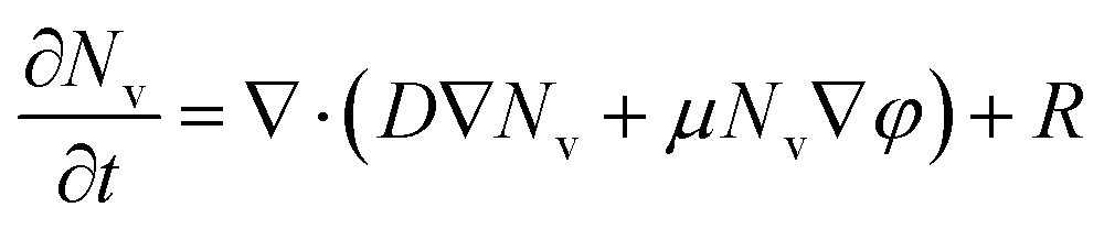 | (1) |
| ∇·σ∇φ = 0 | (2) |
Eqn (2) must be solved prior to eqn (1), and the finite-difference method of the second-order central difference scheme is used on a 51 × 201 2-D square grid. Dirichlet boundary conditions are used. The top boundary is maintained at a positive or negative value, and the other boundaries are kept at zero. In this case, the calculation becomes accurate as the iterations increase, and the solution becomes saturated. Thus, the number of iterations was set to 2000. From this calculation, the potential φ(x, y) can be obtained at a given σ(x, y). eqn (1) is solved through the finite-difference time-domain method using the Crank–Nicolson stencil for the same grid as eqn (2). The Dirichlet and Robin boundary conditions are used. The right and left boundaries always have zero concentration, while the top and bottom boundaries do not allow incoming or outgoing vacancies by diffusion or drift. A sufficiently short interval of time was selected to avoid diversion of the calculation. All parameters are adequately fixed according to the reported data38,44,56,57 and normalized on the basis of qualitative examination. The entire calculation was performed using MATLAB software. The simulation details are explained in the ESI.†
Competing financial interests
The authors declare no competing financial interests.Acknowledgements
This research was supported by the National Research Project for “Next Generation MLC PRAM Development” through the Ministry of Knowledge Economy (MKE) of Korea and by the YSSRC program through Samsung Semiconductor Co.References
- R. Waser and M. Aono, Nat. Mater., 2007, 6, 833–840 CrossRef CAS PubMed.
- A. Sawa, Mater. Today, 2008, 11, 28–36 CrossRef CAS.
- J. J. Yang, M. D. Pickett, X. Li, D. A. A. Ohlberg, D. R. Stewart and R. S. Williams, Nat. Nanotechnol., 2008, 3, 429–433 CrossRef CAS PubMed.
- J. J. Yang, J. Borghetti, D. Murphy, D. R. Stewart and R. S. Williams, Adv. Mater., 2009, 21, 3754–3758 CrossRef CAS.
- J. J. Yang, F. Miao, M. D. Pickett, D. A. A. Ohlberg, D. R. Stewart, C. N. Lau and R. S. Williams, Nanotechnology, 2009, 20, 215201 CrossRef PubMed.
- H. Akinaga and H. Shima, Proc. IEEE, 2010, 98, 2237–2251 CrossRef CAS.
- H. S. P. Wong, H.-Y. Lee, S. Yu, Y.-S. Chen, Y. Wu, P.-S. Chen, B. Lee, F. T. Chen and M.-J. Tsai, Proc. IEEE, 2012, 100, 1951–1970 CrossRef CAS.
- J. J. Yang, D. B. Strukov and D. R. Stewart, Nat. Nanotechnol., 2013, 8, 13–24 CrossRef CAS PubMed.
- Q. Liu, J. Sun, H. Lv, S. Long, K. Yin, N. Wan, Y. Li, L. Sun and M. Liu, Adv. Mater., 2012, 24, 1844–1849 CrossRef CAS PubMed.
- S. Peng, F. Zhuge, X. Chen, X. Zhu, B. Hu, L. Pan, B. Chen and R. W. Li, Appl. Phys. Lett., 2012, 100, 072101 CrossRef PubMed.
- Y. Yang, P. Gao, S. Gaba, T. Chang, X. Pan and W. Lu, Nat. Commun., 2012, 3, 732 CrossRef PubMed.
- R. Waser, R. Dittmann, G. Staikov and K. Szot, Adv. Mater., 2009, 21, 2632–2663 CrossRef CAS.
- Y. Cui, H. Peng, S. Wu, R. Wang and T. Wu, ACS Appl. Mater. Interfaces, 2013, 5, 1213–1217 CAS.
- L. Cario, C. Vaju, B. Corraze, V. Guiot and E. Janod, Adv. Mater., 2010, 22, 5193–5197 CrossRef CAS PubMed.
- A. Brataas, A. D. Kent and H. Ohno, Nat. Mater., 2012, 11, 372–381 CrossRef CAS PubMed.
- A. Chanthbouala, A. Crassous, V. Garcia, K. Bouzehouane, S. Fusil, X. Moya, J. Allibe, B. Dlubak, J. Grollier, S. Xavier, C. Deranlot, A. Moshar, R. Proksch, N. D. Mathur, M. Bibes and A. Barthelemy, Nat. Nanotechnol., 2012, 7, 101–104 CrossRef CAS PubMed.
- J. Yao, Z. Sun, L. Zhong, D. Natelson and J. M. Tour, Nano Lett., 2010, 10, 4105–4110 CrossRef CAS PubMed.
- C. Kügeler, R. Rosezin, E. Linn, R. Bruchhaus and R. Waser, Appl. Phys. A, 2011, 102, 791–809 CrossRef.
- Y. Cui, W. Liu and R. Wang, Phys. Chem. Chem. Phys., 2013, 15, 6804–6808 RSC.
- Y. Takeshi, N. Kazuki, O. Keisuke, K. Masaki, K. Annop, P. Bae Ho and K. Tomoji, Sci. Rep., 2013, 3, 1657 Search PubMed.
- D. S. Jeong, H. Schroeder and R. Waser, Electrochem. Solid-State Lett., 2007, 10, G51–G53 CrossRef CAS PubMed.
- K. J. Yoon, S. J. Song, J. Y. Seok, J. H. Yoon, G. H. Kim, J. H. Lee and C. S. Hwang, Nanotechnology, 2013, 24, 145201 CrossRef PubMed.
- K. J. Yoon, M. H. Lee, G. H. Kim, S. J. Song, J. Y. Seok, S. Han, J. H. Yoon, K. M. Kim and C. S. Hwang, Nanotechnology, 2012, 23, 185202 CrossRef PubMed.
- G. Tang, F. Zeng, C. Chen, H. Liu, S. Gao, C. Song, Y. Lin, G. Chen and F. Pan, Nanoscale, 2013, 5, 422–428 RSC.
- K. J. Yoon, S. J. Song, J. Y. Seok, J. H. Yoon, T. H. Park, D. E. Kwon and C. S. Hwang, Nanoscale, 2014, 6, 2161–2169 RSC.
- K. Tsunoda, Y. Fukuzumi, J. Jameson, Z. Wang, P. Griffin and Y. Nishi, Appl. Phys. Lett., 2007, 90, 113501 CrossRef PubMed.
- Y. C. Huang, H. M. Lin and H. C. Cheng, Int. J. Nanotechnol., 2014, 11, 156–166 CrossRef.
- H. Lim, H. W. Jang, D.-K. Lee, I. Kim, C. S. Hwang and D. S. Jeong, Nanoscale, 2013, 5, 6363–6371 RSC.
- T. Serrano-Gotarredona, T. Masquelier, T. Prodromakis, G. Indiveri and B. Linares-Barranco, Front. Neurosci., 2013, 7, 2 CAS.
- Y. C. Yang, S. Choi and W. Lu, Nano Lett., 2013, 13, 2908–2915 CrossRef CAS PubMed.
- M.-J. Lee, C. B. Lee, D. Lee, S. R. Lee, M. Chang, J. H. Hur, Y.-B. Kim, C.-J. Kim, D. H. Seo, S. Seo, U. I. Chung, I.-K. Yoo and K. Kim, Nat. Mater., 2011, 10, 625–630 CrossRef CAS PubMed.
- L. Zhang, Z. Chen, J. J. Yang, B. Wysocki, N. McDonald and Y. Chen, Appl. Phys. Lett., 2013, 102, 153503–153504 CrossRef PubMed.
- W. Wang, S. Fujita and S. S. Wong, IEEE Electron Device Lett., 2009, 30, 763–765 CrossRef CAS.
- F. Miao, J. J. Yang, J. Borghetti, G. Medeiros-Ribeiro and R. S. Williams, Nanotechnology, 2011, 22, 254007 CrossRef PubMed.
- P. Sang-Joon, L. Jeong-Pyo, J. Jong Shik, R. Hyun, Y. Hyunung, Y. Byung Youn, K. Chang Soo, K. Kyung Joong, C. Yong Jai, B. Sunggi and L. Woo, Nanotechnology, 2013, 24, 295202 CrossRef PubMed.
- Y. Li, H. Lv, Q. Liu, S. Long, M. Wang, H. Xie, K. Zhang, Z. Huo and M. Liu, Nanoscale, 2013, 5, 4785–4789 RSC.
- H. Jiang and Q. Xia, Nanoscale, 2013, 5, 3257–3261 RSC.
- S. Larentis, F. Nardi, S. Balatti, D. C. Gilmer and D. Ielmini, IEEE Trans. Electron Devices, 2012, 59, 2468–2475 CrossRef.
- S. Balatti, S. Larentis, D. C. Gilmer and D. Ielmini, Adv. Mater., 2013, 25, 1474–1478 CrossRef CAS PubMed.
- Y. Yang, P. Sheridan and W. Lu, Appl. Phys. Lett., 2012, 100, 203112 CrossRef PubMed.
- Y. C. Bae, A. R. Lee, J. S. Kwak, H. Im, Y. H. Do and J. P. Hong, Appl. Phys. A: Mater. Sci. Process., 2011, 102, 1009–1013 CrossRef CAS PubMed.
- K. M. Kim, S. Han and C. S. Hwang, Nanotechnology, 2012, 23, 035201 CrossRef PubMed.
- D. Ielmini, F. Nardi and S. Balatti, IEEE Trans. Electron Devices, 2012, 59, 2049–2056 CrossRef CAS.
- S. M. Yu and H. S. P. Wong, IEEE Electron Device Lett., 2010, 31, 1455–1457 CrossRef CAS.
- I. Salaoru, A. Khiat, Q. J. Li, R. Berdan, C. Papavassiliou and T. Prodromakis, J. Phys. D: Appl. Phys., 2014, 47, 10 CrossRef.
- M. Noman, A. A. Sharma, Y. M. Lu, R. Kamaladasa, M. Skowronski, P. A. Salvador and J. A. Bain, Appl. Phys. Lett., 2014, 104, 5 CrossRef PubMed.
- T. Tamura, S. Ishibashi, K. Terakura and H. M. Weng, Phys. Rev. B: Condens. Matter Mater. Phys., 2009, 80, 195302 CrossRef.
- P. Woo Young, K. Gun Hwan, S. Jun Yeong, K. Kyung Min, S. Seul Ji, L. Min Hwan and H. Cheol Seong, Nanotechnology, 2010, 21, 195201 CrossRef PubMed.
- J. J. Huang, C. W. Kuo, W. C. Chang and T. H. Hou, Appl. Phys. Lett., 2010, 96, 262901 CrossRef PubMed.
- J. S. Kwak, Y. H. Do, Y. C. Bae, H. S. Im, J. H. Yoo, M. G. Sung, Y. T. Hwang and J. P. Hong, Appl. Phys. Lett., 2010, 96, 223502 CrossRef PubMed.
- K. M. Kim, B. J. Choi, D. S. Jeong, C. S. Hwang and S. Han, Appl. Phys. Lett., 2006, 89, 162912 CrossRef PubMed.
- F. Gomez-Marlasca, N. Ghenzi, M. J. Rozenberg and P. Levy, Appl. Phys. Lett., 2011, 98, 042901 CrossRef PubMed.
- Y. H. Do, J. S. Kwak, Y. C. Bae, J. H. Lee, Y. Kim, H. Im and J. P. Hong, Curr. Appl. Phys., 2010, 10, e71–e74 CrossRef PubMed.
- Y. B. Nian, J. Strozier, N. J. Wu, X. Chen and A. Ignatiev, Phys. Rev. Lett., 2007, 98, 146403 CrossRef CAS.
- H. Y. Jeong, J. Y. Lee, S. Y. Choi and J. W. Kim, Appl. Phys. Lett., 2009, 95, 162108 CrossRef PubMed.
- S. Kim, S. J. Kim, K. M. Kim, S. R. Lee, M. Chang, E. Cho, Y. B. Kim, C. J. Kim, U. I. Chung and I. K. Yoo, Sci. Rep., 2013, 3, 1680 Search PubMed.
- S. Kim, S. Choi and W. Lu, ACS Nano, 2014, 8, 2369–2376 CrossRef CAS PubMed.
- V. Rana and R. Waser, in Memristors and Memristive Systems, ed. R. Tetzlaff, Springer, New York, 2014, pp. 223–251 Search PubMed.
Footnote |
| † Electronic supplementary information (ESI) available. See DOI: 10.1039/c4ra09443c |
| This journal is © The Royal Society of Chemistry 2015 |