Experimental and simulative study on surface enhanced Raman scattering of rhodamine 6G adsorbed on big bulk-nanocrystalline metal substrates

Zao Yiab, Yong Yib, Jiangshan Luoc, Xin Yebc, Pinghui Wud, Xiaochun Jibc, Xiaodong Jiangc, Yougen Yi*a and Yongjian Tang*bc
aCollege of Physics and Electronics, Central South University, Changsha 410083, Hunan, China. E-mail: yougenyi@mail.csu.edu.cn; Fax: +86 0816 2480830; Tel: +86 0816 2480827
bJoint Laboratory for Extreme Conditions Matter Properties, Southwest University of Science and Technology and Research Center of Laser Fusion, Mianyang 621010, Sichuan, China. E-mail: myyz1984@mail.csu.edu.cn; Fax: +86 0816 2480830; Tel: +86 0816 2480827
cResearch Center of Laser Fusion, China Academy of Engineering Physics (CAEP), Mianyang 621900, Sichuan, China
dState Key Laboratory of Modern Optical Instrumentation, Department of Optical Engineering, Zhejiang University, Hangzhou 310027, Zhejiang, China

Received 23rd June 2014 , Accepted 17th November 2014

First published on 18th November 2014


Abstract

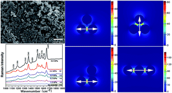
Big bulk-nanocrystalline metal materials of silver (Ag) and aluminum (Al) for surface-enhanced Raman scattering (SERS) spectroscopy have been synthesized in a mold under different pressures using vacuum-warm-compaction technology. It was discovered that pressure could control the SERS activity of the bulk-nanocrystalline material. SERS properties of the bulk-nanocrystalline material in the presence of adsorbed rhodamine (R6G) could be obtained through selecting a proper pressure. Compared with the Ag nanoparticles (Al nanoparticles), the SERS peak intensity of R6G adsorbed on the bulk-nanocrystalline material is about 1000 times (100 times) stronger. The electric field enhancement of the bulk-nanocrystalline material has been described to be a systematic investigation by using three-dimensional finite-difference time-domain (3D-FDTD) simulation. The FDTD calculations have shown that the electric field enhancement of the bulk-nanocrystalline material is strongly dependent on the gap distance. In summary, SERS active bulk-nanocrystalline materials have been synthesized simply, greenly and cost effectively by the method reported here, and this method is expected to be utilized in the development of SERS-based analytical devices.


1. Introduction

Since enhanced Raman signals have been discovered on the surface of metals and metal compounds with metal decoration (such as Ag, Au, Al, Cu), the surface enhanced Raman scattering (SERS) technique has been implemented widely by a broad scientific research community for chemical and measurements and biological sensing.1–3 As a sensitive exploration technique, SERS has the ability to give lots of information about the character of adsorbed molecules, even single molecules.4,5 The mechanism of SERS includes two main mechanisms. They are the chemical (CM) mechanism6 and the electromagnetic (EM) mechanism.7 In these investigations, the CM enhancement is mainly due to the charge transfer between the metal and adsorbed molecules. However, the EM mechanism is though to contribute the most for SERS. The EM enhancement is due to the enhanced local electric field at the surface of a metal that in order to an important increase in the cross section of the Raman scattering.8,9 The EM enhancement is depended by many factors, including the shape, dielectric environment, metal type and aggregation state.10–12 The enormous enhancement of the SERS, even single molecule SERS, is generally believed to originate from the “hot spots” on the junction of two or more aggregated metal nanostructures.13,14 The closely distance nanostructures about 1 nm could offer an enhancement of 1010 at the junction of two nanostructures.15 At the same time, field enhancement for SERS from metal nanostructure also has been researched by many theoretical works.16–18

These “hot-spots” induced in the gaps between the nanostructures have been studied by many theoretical and experimental researches. And the “hot-spots” have major contribution to the Raman enhancement.19 Many researches have implied that some complex geometries could provide the extremely EM coupling, and then get a strong enhancement factor. These complex geometries include aggregated nanoparticles,20 spongelike network21 and branchlike structures.22 Through comparing with the isolated and individual nanostructure arrays, these complex geometries can provide lots of “hot spots” because of abundant contacts. The high quality SERS substrate can be produced by these routes. The complex geometries system's plasmon coupling phenomenon has been mentioned extensively by the theories and experiments. For SERS, we hope to synthesize the high SERS active substrates. And we can easily adjust and control the substrates' SERS activity.

Here, in this research, we report a vacuum-warm-compaction (VWC) technology to synthesize activity tunable SERS substrates. The bulk-nanocrystalline's SERS activity could be adjusted and controlled through different pressure easily. Because we didn't have any chemical in the synthesis of the metal nanoparticles and bulk-nanocrystalline using flow-levitation method (FL) and VWC technology, it is advantageous for synthesizing chemically pure SERS substrates. We have adjusted he bulk-nanocrystalline' SERS properties through selecting different pressure. We have studied the effect of the enhancement factor (EF) that comes from the nanoparticles trimers through 3D-FDTD simulation, also. The experimental and simulation results have shown that the bulk-nanocrystalline have shown a high reproducibility and extremely SERS enhancement because lots of “hot spots” can form at the gaps.

2. Experimental details

Ag nanoparticles and Al nanoparticles were prepared by the FL method in our previous papers.23,24 The Fig. 1 is the scheme of the FL method for synthesizing Ag nanoparticles and Al nanoparticles. The desired bulk-nanocrystalline-Ag and bulk-nanocrystalline-Al could be synthesized in a mold with different pressures by using VWC technology. Because it could induce the inert gases desorption in order to accelerate atoms spread. So the VWC technique can improve the flow-levitation-cold compaction way effectively.25 The process of VWC technique is including three steps. The first one is that we synthesized the metal nanoparticles through FL way. The second one is that we loaded the metal nanoparticles into the glove box. The last one is that we prepared the metal bulk-nanocrystalline through VWC technique. Ag or Al nanoparticles were filled into the mold, and the experiment was completed in vacuum-glove-chest (ZKSTX-1 type) with Ar protection. After that, we put the mold into the ZM-18-10Y type vacuum-hot-press. And then, we pumped the pressure of chamber to 0.005 MPa. For releasing absorbed gas before the pressing, we heated the mold about 30 min. At last, we compacted the nanoparticles by 0.2–1.0 GPa pressure. The temperature is 523 K, and the duration time is 30 min.
image file: c4ra06141a-f1.tif
Fig. 1 The scheme of the flow-levitation method for synthesizing metal nanoparticles.

For SERS spectra measurements, first of all, by using an accurate pipette, we dropped a 10 μL droplet of R6G aqueous solution (different concentration) on the samples. Secondly, let the samples dried in air at ambient temperature, in order to gain a uniform molecule deposition over an area of about 10 mm2. In this experiment, three SERS-active substrates of the same samples were prepared, and at least 10 different points on each substrate were selected to detect the R6G probes, to verify the stability and reproducibility of these SERS-active substrates. We used Renishaw inVia microscopy Raman spectroscopy which includes a CCD detector and a holographic notch filter to measure SERS spectra. The SERS was excited by using radiation of 514.5 or 632.8 nm which was about 7.2 mW at the position of samples. Here, in our experiment, the obtained sampling volume is the product of the area of the laser spot (∼1 μm in diameter) and the penetration depth (∼2 μm) of the focused laser beam. The recorded time of the Raman spectra is 20 s.

3. Simulation methods

In present, many numerical techniques are available to calculate the electric field distribution of nanostructures, such as the discrete dipole approximation (DDA), the boundary element method (BEM), the finite element method (FEM) and the FDTD method.26–29 Among these numerical techniques, the FDTD is the most used method for the calculation of the electric field distribution on metal nanostructures.29–31 We used a commercial FDTD calculation for 3D-FDTD simulations.32 Perfectly matched layer (PML) absorbing boundaries were used for the simulation. The calculation region is 0.3 × 0.3 × 0.14 μm3, and the cell size is 1 × 1 × 1 nm3. We installed propagation directions of plane waves with different wavelength. Because the distribution of nanoparticles is random in the bulk-nanocrystalline metal materials, for compute simple, we only analyzed the distributions of electric field intensity of trimers with different gap. The Fig. 2 has shown the schematic geometries of the structures studied in this paper. The types of trimers are including V-shaped trimer (x and y), L-shaped trimer and linear shaped trimer. The diameter (d) of the nanoparticles was set to 60 nm, corresponding to that of the nanoparticles used in our experiments. The parameter g is the gap distance between nanoparticles. We set the simulation time to be 300 fs, and input pulse width is 14.70 fs in order to ensure the fields decay completely. We set the refractive index of surrounding medium as 1.0 for air. These Ag and Al nanoparticles were free-floating in air, no substrates. The Ag and Al nanoparticles' dielectric constant came from Palik's experimental data.33 We express the near-field intensity enhancement images. They are set up by dividing the electric field strength (E2 = Ex2 + Ey2 + Ez2) around the models. In the simulation, first of all, we calculate the local electric field. And then evaluate the field intensity for each mesh through integration. At last we compare the computation with the EF values which come from the measured Raman spectra.
image file: c4ra06141a-f2.tif
Fig. 2 Schematic of the trimers: (A–B) V-shaped trimer; (C) L-shaped trimer; (D) linear trimer.

4. Results and discussion

Fig. 3A is the typical TEM patterns of Ag nanoparticles prepared through FL method. From the picture, we know that these nanoparticles are spherical. And all the nanoparticles display a black color. The diameter of the nanoparticles is 5–100 nm. Because we have not used capping agent in this experiment, some nanoparticles have appeared aggregate with each other. The metal nanoparticles' size distribution was computed from TEM images using Image-Pro plus 5.0, as shown Fig. 3B. From the picture, we know that the nanoparticles' size distribution is narrow (40–80 nm). And the nanoparticles' average diameter is about 60 nm. The bulk-nanocrystalline-Ag (0.6 GPa) is disc-shaped, and the diameter is 10 mm, as shown the typical optical image (Fig. 3C). The pressure can control the bulk-nanocrystalline's relative density through the VWC technique. At the beginning of the compaction process, the increase of density is obvious with the pressure increasing. At this stage, densification is driven by the motion of particles and the filling of void among particles. When the pressure continues to increase, the nanoparticles will deform. The deformation of the particles begins at the contact area of transfer pressure particles. The contact area of stress must exceed the yield limit of the material in order to ensure further denseness.25 In our experiment, the pressure is 1.0, 0.8, 0.6, 0.4 and 0.2 GPa, respectively. The Fig. 4 shows the products' SEM images. When the pressure increases, the gap distances of nanoparticles decrease. Fig. 4D shows the morphology of Ag nanoparticles. These Ag nanoparticles are spherical.
image file: c4ra06141a-f3.tif
Fig. 3 (A) TEM images of the Ag nanoparticles; (B) the size distribution of Ag nanoparticles estimated from TEM images; (C) optical image of the bulk-nanocrystalline-Ag.

image file: c4ra06141a-f4.tif
Fig. 4 SEM images of the bulk-nanocrystalline composed of Ag nanoparticles made with (A) 0.2, (B) 0.6, (C) 1.0, and (D) 0 GPa pressure, respectively.

The SERS activity of the bulk-nanocrystalline-Ag was evaluated by using R6G as the probing adsorbate. Bulk-nanocrystalline-Ag at various pressures was used as the SERS samples in order to estimate SERS contribution. The contribution came from the “hot spots” of bulk-nanocrystalline-Ag. Fig. 5A shows the SERS spectrum of R6G (1 × 10⁻¹⁰ M) with different samples (bulk-nanocrystalline-Ag prepared various pressures and Ag nanoparticles). The excitation source is 514.5 nm. From the spectra curve, lots of peaks are expressly observed. These remarkable peaks could be assigned to the aromatic stretching vibration that at 1361, 1506 and 1649 cm−1.34 Based on our previous researches about the SERS quality for the SERS substrates,35,36 the enhancement factor (EF) for different samples were roughly estimated by comparing the peak intensity at 1649 cm−1, as shown Fig. 5B. The enhancement factor (EF) values of R6G in the nanoparticles are calculated the following expression:

 
image file: c4ra06141a-t1.tif(1)
ISERS is the enhanced intensity of the adsorbed R6G molecules on the SERS substrate. The value of ISERS mainly arises from a single molecule layer covering a nanoparticle array, from which other additional molecule layers of analytes on the SERS substrate, as previously reported,35 do not contribute to Raman gain and can be neglected. IRef is the spontaneous Raman scattering intensity from the bulk R6G molecules under the laser spot on the blank glass substrate. NSERS is the number of the single-layer molecules covering the SERS substrate under the laser spot. NRef is the number of the bulk molecules excited by laser on the surface of the regular substrate. In order to obtain the values of these four parameters, we follow the same procedures based on the published literatures.35,36 Using the 50× objective lens, we determine the area of the laser spot size at around 1 μm2. We also calculate the area of a single molecule of R6G to be approximately 1 × 10⁴ nm2. Thus, the value of NSERS under the laser excitation is approximately 1 × 10² molecules. The focusing scope of laser beam is approximately 5 μm, thus scattering from all R6G molecules underneath the laser spot is detected. Assuming a uniform distribution of R6G over the droplet area of 2 mm2, the value of NRef is approximately 1.5 × 10⁷ molecules. Therefore, from the equation, the EF is simply (1.5 × 10⁵) × (ISERS/IRef). Then, the intensity of the peak at 1649 cm−1 (EF) is following 4.8 × 10⁷ for different samples (0 GPa), 8.5 × 10⁸ (0.2 GPa), 3.6 × 10⁹ (0.4 GPa), 1.4 × 10¹⁰ (0.6 GPa), 1.1 × 10⁹ (0.8 GPa) and 4.3 × 10⁸ (1.0 GPa), respectively. The SERS signal of R6G on the bulk-nanocrystalline-Ag (0.6 GPa) substrate is about 1000 times stronger than that on the Ag nanoparticles substrate by using 514.5 nm radiation as excitation source. So the bulk-nanocrystalline-Ag has two advantages that one is easy of using, another is give extremely SERS signals. When the R6G molecules have adsorbed on bulk-nanocrystalline-Ag, the intensity of the peak at 1649 cm−1 has changed with the different pressure, as shown in Fig. 5B. This phenomenon has indicates that the bulk-nanocrystalline-Ag's SERS activity could be controlled through different pressure. From these curve, we have known that the bulk-nanocrystalline-Ag prepared by 0.6 GPa of pressure has the largest SERS intensity. When the pressure increased in the bulk-nanocrystalline-Ag, the intensity of the “hot spots” does not always increase automatic, as shown in Fig. 5. When the pressure continues to increase (from 0.6 to 1.0 GPa), the SERS intensity begins to decrease. This phenomenon can be attributed to the different gaps among the particles, the change of the number of effective gaps, the different numbers of adsorbates irradiated by the laser light, and different morphologies of the particles. It is well known that the crevices or gaps between two or three particles in contact with one another are hot sites for the induction of SERS via an electromagnetic enhancement mechanism.37,38 For a gap of 1 nm between two Ag spheres with the diameter of 90 nm, the EF was estimated to be ∼1010 in a volume that could contain only a few molecules.38 When two particles approach each other, their transition dipoles are expected to couple in such a way that the enhanced electromagnetic fields around each particle can create a pattern of coherent interference. When the gaps among the particles decrease with the increase in pressure, the coupled plasmon resonance shifts to red, and the enhanced electromagnetic field increases at the junction of the particles.39 Moreover, the numbers of effective gaps will also increase along with the decrease of the gaps. In addition, the signal increase observed is thought to occur likely from the increase in the number of adsorbates irradiated by the laser light. Compared with the gap distance of the Ag nanoparticles by man pressure accumulation, the gap distance of the bulk-nanocrystalline-Ag prepared by mechanical press is smaller. So, the bulk-nanocrystalline-Ag's SERS intensity is greater than the Ag nanoparticles' SERS intensity. The SERS enhancement probably related to the following factors. First of all, the morphology of SERS substrates can be recognized to contribute for the enhancement properties.40 In conclusion, the sharpest surface features can induce the greater field enhancements. When the pressure increases, the bulk-nanocrystalline-Ag's particle morphology becomes more planar in order to the particles' morphology changes from 3D to 2D. The change of morphology can induce the greater localized field enhancement because of the lightning rod effect. However, localized field enhancement becomes weaker when the lager pressure is used on the bulk-nanocrystalline. So, when the pressure is changed from 0.6 to 1.0 GPa, the bulk-nanocrystalline-Ag's SERS intensity decreases. When the pressure is under 0.6 GPa, the particles' gap distance prevents electromagnetic enhancement. So the bulk-nanocrystalline's gap distance can play an important effect when the pressure changed from 0.6 to 1.0 GPa. Secondly, the influence of the tunneling charge transfer between nanoparticles should be considered, also. When the gap distance between the nanoparticles was decreased under 1 nm, the enhancement of SERS can decrease because the particle plasmon emission reduces through tunneling electrons.41,42 The tunneling charge transfer has appeared at the metal–molecule–metal junctions with charge difference density.43 Once the pressure becomes large enough, the nanoparticles will be flattened in order to connect with each other. And the gaps' “hot spots” will decrease. So, the intensity of SERS spectroscopy will decrease because the lightning rod effect decreased.


image file: c4ra06141a-f5.tif
Fig. 5 (A) SERS spectra of R6G (1 × 10⁻¹⁰ M) adsorbed on the Ag nanoparticles and on bulk-nanocrystalline-Ag composed of Ag nanoparticles made with 0.2, 0.4, 0.6, 0.8 and 1.0 GPa, respectively using 514.5 nm radiation as an excitation source. (B) The normalized SERS peak intensity of the ∼1649 cm−1 band of R6G adsorbed on the bulk-nanocrystalline-Ag composed of Ag nanoparticles and Ag nanoparticles using 514.5 nm radiation as an excitation source.

Here, Al nanoparticles were used to synthesize bulk-nanocrystalline-Al, although they have very weak SERS activity.44 In this work, the pressure of synthesized bulk-nanocrystalline-Al is 1.0, 0.8, 0.6, 0.4 and 0.2 GPa, respectively. The concentration of R6G is 10−5 M. As shown Fig. 6, the peak intensity at 1649 cm−1 is following for different samples 8.3 × 10³ (0 GPa), 4.9 × 10⁴ (0.2 GPa), 8.1 × 10⁵ (0.4 GPa), 7.5 × 10⁴ (0.6 GPa), 6.1 × 10⁴ (0.8 GPa) and 9.4 × 10³ (1.0 GPa), respectively. The maximum value of the SERS peak intensity appears at 0.4 GPa pressure, and this value is about 100 times greater than when it is adsorbed on the Al nanoparticles, using 514.5 nm radiation as an excitation source. This indicates that the method of preparing activity-tunable substrates by pressure for SERS spectroscopy is applicable over a wide range.


image file: c4ra06141a-f6.tif
Fig. 6 The normalized SERS peak intensity of the ∼1649 cm−1 band of R6G (1 × 10⁻³ M) adsorbed on the bulk-nanocrystalline-Al composed of Al nanoparticles and Al nanoparticles using 514.5 nm radiation as an excitation source.

Fig. 7 shows the SERS spectrum of R6G with different concentration (10−9, 10−10, 10−11, 10−12 and 10−13 M) on bulk-nanocrystalline-Ag (0.6 GPa). The SERS signal intensities will decrease when the concentration decreases. However, we can still watch the signals at a concentration as low as 10−13 M. These “hot spots” can induce the electric field enhancement in order to provide the extremely SERS. These “hot spots” may come from gaps and vacancies in the bulk-nanocrystalline-Ag.


image file: c4ra06141a-f7.tif
Fig. 7 Typical SERS spectra of R6G with different concentration on bulk-nanocrystalline-Ag (0.6 GPa).

The 3D-FDTD method was applied to compute the electromagnetic field distribution which surrounds the laser-illuminated bulk-nanocrystalline-Ag by numerically solving Maxwell's equations,45,46 in order to further indicate the physical mechanism of SERS enhancements of the bulk-nanocrystalline-Ag. The local field enhancing has a key and necessary factor that plasmonic coupling between adjacent nanoparticles.47 The “hot spots” will appear at the gap area of the dimer when two or more metal nanoparticles contact to each other.48 Here, in the actual situation of our research, lots of nanogaps could be formed between the adjacent nanoparticles. The distributions of electric field intensity in three types of aggregation topologies of nanoparticles trimers: V-shaped trimer (x and y), L-shaped trimer and linear shaped trimer. Fig. 8A–H presents calculated electric field enhancement distribution of V-shaped trimer (x) with different gap distance: 0, 2, 5, 10, 30, 60, 80 and 100 nm, respectively. The diameter of Ag particles is 60 nm. The incoming light is polarized along the x-axis. The excitation wavelength is 514.5 nm. As shown in Fig. 8B, the maximal electric field strength (|E|/|E0|)2 of 5.6 × 10³ can be obtained when a small gap appeared between two Ag nanoparticles (such as 2 nm). However, the maximal field strength's value is about 610 when the distance of gap was 5 nm (Fig. 8C). Compared with the right column of Fig. 8B, the value is about 10.9% of the maximal electric field strength with 2 nm gap. The plasmonic coupling between the nanoparticles with suitable gap can provide the high electric field. The high electric field can offer the largest Raman scattering enhancements for some molecules presenting in the gap. These SERS “hot spots” with very sensitivity can achieve the single molecule detection. However, the maximal field strength's value is about 12.4 when the space of nanogaps was 100 nm (Fig. 8H), which is not significantly improved over that obtained from isolated Ag nanoparticles (shown in the right column of Fig. 13A), representing weak field enhancement within the gap. It means that the plasmon interaction is quite weak in such case due to the field attenuation deviating from either side of the gap. These results are important for SERS on nanostructure assemblies. The reason is that the gap regions between the adjacent nanoparticles do not provide “hot spots” through resonant excitation. Optical signal enhancements could just be realized through exciting the bonding plasmon mode. When the gap size is decreased to ∼30 nm or less (Fig. 8E), the plasmon interaction effect appears. The “hot spot” numbers start to increase drastically. For SERS, it is widely believed that |(|E|/|E0|)|4 is the factor for the Raman intensity increases.49 The maximum SERS enhancements on the eight models of V-shaped trimer (x) correspond to 6.8 × 10⁶, 3.1 × 10⁷, 3.7 × 10⁵, 1.5 × 10⁴, 5.8 × 10², 2.6 × 10², 2.0 × 10² and 1.7 × 10², respectively. As a result, the Raman signal intensity starts to increase. Because of the small gap distance between the nanoparticles, localized surface plasmons from each nanostructure are strongly coupled and thereby significantly enhance the field in the gap, providing lots of “hot spots” to detect the Raman molecule.


image file: c4ra06141a-f8.tif
Fig. 8 (A–H) E-field intensity from theoretical calculations at the excitation wavelength of 514.5 nm for V-shaped trimer (x) with different gap distance: 0, 2, 5, 10, 30, 60, 80 and 100 nm, respectively. The diameter of Ag nanoparticles is 60 nm. The arrows represent the polarization directions parallel x axis.

Here, we have studied the relationship of gap distance and excitation wavelength, as shown in Fig. 9A. The model is V-shaped trimer (x). The incoming light is polarized along the x-axis. Compared the curve of the Fig. 9A, the SERS enhancement's qualitative tendencies are the same when the incident light is 632.8 or 514.5 nm. As shown in Fig. 9B, through these calculations, we systemic shown pressure dependent SERS enhancement on different excitation wavelength, in order to research the relationship of fabricated structures' SERS enhancement and excitation wavelength. From the maximum field enhancement's ((|E|/|E0|)2) 3D-FDTD calculations, it is can be found that the EF of V-shaped trimer (x) different excitation wavelengths increased in a series: 514.5 > 488 > 568 > 632.8 > 782 nm. As mentioned previously, when the wavelength of the incoming light is adjacency to the V-shaped trimer (x) Ag nanoparticles' localized surface plasmon resonance wavelength, the favorable electromagnetic coupling will appear. So, it is conceivable that the 514.5 nm excitation source will yield a highest SERS activity.


image file: c4ra06141a-f9.tif
Fig. 9 (A) Simulated maximal field enhancement (|E|2) according to the different gap distance; (B) Simulated maximal field enhancement (|E|2) according to the different excitation wavelengths: 488, 514.5, 568, 632.8 and 782 nm.

With different polarization directions, the incoming light can excite various plasmons at the same conditions.50 As shown Fig. 8 and 10, the (|E|/|E0|)2 values can be decreased, once the incoming light is polarized along the y-axis. The near field distribution of the V-shaped trimer (x) is symmetrical along the long axis' direction, when the polarization parallel to the long axis (x-axis), such as the column in Fig. 8. The reason is that the coupled Ag nanoparticles have a dipole-like localized surface plasmon coupling character. However, as shown in Fig. 10, the symmetry of field distribution can convey from one side of the V-shaped trimer (y) to the other side when the polarization direction is parallel to the y-axis. When polarization direction of V-shaped trimer was changed, the localized surface plasmon coupling was distributed evenly. The “delocalization” and distribution of localized surface plasmon coupling may suppress EF enhancement. The reason is that a parallel orientation of localized surface plasmon coupling with polarization is indispensable for obtaining the strongest light intensity.51 So, the polarization direction of incident light can distinctly control the V-shaped trimer's surface plasmonic field distribution.


image file: c4ra06141a-f10.tif
Fig. 10 (A–H) E-field intensity from theoretical calculations at the excitation wavelength of 514.5 nm for V-shaped trimer (y) with different gap distance: 0, 2, 5, 10, 30, 60, 80 and 100 nm, respectively. The diameter of Ag particles is 60 nm. The arrows represent the polarization directions parallel y axis.

Fig. 11A–H presents calculated electric field enhancement distribution of L-shaped trimer with different gap distance: 0, 2, 5, 10, 30, 60, 80 and 100 nm, respectively. The diameter of Ag particles is 60 nm. The incoming light is polarized along the x-axis. The excitation wavelength is 514.5 nm. The change tendencies of maximal electric field strength (|E|/|E0|)2 are the same at the V-shaped trimer. As shown in Fig. 11B, when the gap distance is 2 nm, the maximal electric field strength (|E|/|E0|)2 is about 3.2 × 10³ at the adjacent nanoparticles. The localized surface plasmon coupling is very weak to be negligible between the nanoparticles when the gap distance is 100 nm, and electromagnetic enhancements are come from the isolated particles.


image file: c4ra06141a-f11.tif
Fig. 11 (A–H) E-field intensity from theoretical calculations at the excitation wavelength of 514.5 nm for L-shaped trimer with different gap distance: 0, 2, 5, 10, 30, 60, 80 and 100 nm, respectively. The diameter of Ag particles is 60 nm. The arrows represent the polarization directions parallel x axis.

As shown in Fig. 11B–H, it is well known that the electromagnetism's coupling effect can be gradually enhanced with the decrease of gap distance. However, compared with V-shaped trimer (x), the maximal electric field strength (|E|/|E0|)2 is decreased with same gap distance. The L-shaped Au nanoparticles's linear and second order nonlinear optical characteristics have studied by Canfield and co-workers.52,53 They have shown that the polarization directions can induce the L-shaped nanoparticle's linear and second harmonic generation response. The extinction spectra have two optical transitions that including independent polarizations along the substrate plane and perpendicular to the substrate plane. L-shaped trimer has two main optical transitions, and the nonpolarized transition can induce the main transitions' blue. Each polarized resonance had its resonance wavelength. So, compared with V-shaped trimer (x), the maximal electric field strength (|E|/|E0|)2 of L-shaped trimer is decreased.

Fig. 12A–H presents calculated electric field enhancement distribution of linear shaped trimer with different gap distance: 0, 2, 5, 10, 30, 60, 80 and 100 nm, respectively. The diameter of Ag particles is 60 nm. The incoming light is polarized along the x-axis. The excitation wavelength is 514.5 nm. Here, compared with V-shaped trimer (x), as shown Fig. 8A–H, the maximal electric field strength (|E|/|E0|)2 is increased with same gap distance. For example, as shown the Fig. 12B, the maximal electric field strength (|E|/|E0|)2 at the junction of particles is about 6.4 × 10³ that lager the 5.6 × 10³ (Fig. 8B). The linear shaped trimer can provide the largest electromagnetic field when the incoming light is polarized along the x-axis. There are two contributions for the electromagnetic field that including dipolar plasmon resonance and so-called “the lightning rod effect”. It is well known that the high curvature of nanorod ends could induce the extremely electromagnetic fields. And the extremely enhancements provided by “the lightning rod effect” have important contribution for SERS.54 As shown these figures (from Fig. 8 to 12), compared with the gap = 2 nm, the value of the maximal electric field strength with 0 nm gap is less. The numerical simulation by classical Maxwell EM wave theory is no longer valid once the gap size is 0 nm. In our next study, we will introduce quantum mechanics to study the field enhancement at 0 nm.


image file: c4ra06141a-f12.tif
Fig. 12 (A–H) E-field intensity from theoretical calculations at the excitation wavelength of 514.5 nm for linear trimer with different gap distance: 0, 2, 5, 10, 30, 60, 80 and 100 nm, respectively. The diameter of Ag particles is 60 nm. The arrows represent the polarization directions parallel x axis.

Fig. 13 shows calculated electric field enhancement distribution of isolated Ag, isolated Al and Al trimers with different shape. The diameter of metal nanoparticles is 60 nm. The incoming light is polarized along the x-axis. We chose the excitation wavelength of ∼514.5 nm for the calculation, because it is used for the excitation source for SERS measurement. Fig. 13A and B show the electric field enhancement distribution around isolated Ag and Al nanoparticle with the same condition. A comparison of Fig. 13A with 13B clearly shows the maximal electric field strength (|E|/|E0|)2 generated around the Ag nanoparticle are stronger than that of Al nanoparticle. Fig. 13C–F shows the electric field enhancement distribution of the Al trimers system. The gap distance is 10 nm. The EF of four models increase in a series: V-shaped trimer (y) < L-shaped trimer < V-shaped trimer (x) < linear trimer, on the basis of the 3D-FDTD calculation results of the maximum field enhancement ((|E|/|E0|)2). Because of dipolar plasmon resonance and “the lightning rod effect”, Al linear trimer has the maximal electric field strength (|E|/|E0|)2 at the junction of particles (Fig. 13C–F, EF = 40). Compared with Ag trimers, the maximal electric field strength (|E|/|E0|)2 is obvious decreased with same gap distance. These reasons are that Ag nanoparticles's resonance property lie in the visible regime, and Ag nanoparticles's resonance property is blue shifted to the UV range.55,56


image file: c4ra06141a-f13.tif
Fig. 13 E-field intensity from theoretical calculations at the excitation wavelength of 514.5 nm for (A) isolated Ag; (B) isolated Al; (C–F) Al trimers with different shape, gap distance is 10 nm. The diameter of nanoparticles is 60 nm.

5. Conclusions

In summary, we have shown that the bulk-nanocrystalline of Ag and Al can be synthesized simply, green and cost effectively using VWC technology. The bulk-nanocrystalline exhibits a high quality SERS property. The bulk-nanocrystalline' SERS properties could be controlled through selecting different pressure. A maximum enhancement factor of 1.4 × 10¹⁰ can be obtained with the bulk-nanocrystalline-Ag (0.6 GPa). The 3D-FDTD calculations indicate that the bulk-nanocrystalline may demonstrate a high quality SERS property owing to the gap distance. When the gap distance of the trimer is decreased to ∼30 nm or less, the plasmon interaction of nanoparticles effect appears, and the numbers of “hot spots” start to increase drastically. It can be found that the EF of four models increased in a series: V-shaped trimer (y) < L-shaped trimer < V-shaped trimer (x) < linear trimer. The EF of V-shaped trimer (x) different excitation wavelengths can be found to increase in a series: 514.5 > 488 > 568 > 632.8 > 782 nm. The present work can provide a possibility of applying that environment friendly bulk-nanocrystalline can provide significant electric field strength and further increase the enhancement factor. We hope that the way can provide helpful guidelines for the development of SERS properties.

Acknowledgements

The work is supported by the National Natural Science Foundation of China (no. 10804101; 60908023; 11375159), and the Science and Technology Development Foundation of Chinese Academy of Engineering Physics (Grant no. 2010B0401055), and the Scholarship Award for Excellent Doctoral Student granted by Ministry of Education (1343-76140000014), and the Hunan Provincial Innovation Foundation For Postgraduate (Grant no. CX2012B114), and the Open-End Fund for the Valuable and Precision Instruments of Central South University (CSUZC2012032).

References

  1. Y. W. C. Cao, R. C. Jin and C. A. Mirkin, Nanoparticles with Raman Spectroscopic Fingerprints for DNA and RNA Detection, Science, 2002, 297, 1536–1540 CrossRef CAS PubMed.
  2. J. N. Anker, W. P. Hall, O. Lyandres, N. C. Shah, J. Zhao and R. P. Van-Duyne, Biosensing with plasmonic nanosensors, Nat. Mater., 2008, 7(6), 442–453 CrossRef CAS PubMed.
  3. Z. Yi, J. S. Luo, X. B. Li, Y. Yi, X. B. Xu, P. H. Wu, X. D. Jiang, W. D. Wu, Y. G. Yi and Y. J. Tang, Plasmonic Coupling Effect in Silver Spongelike Networks Nanoantenna for Large Increases of Surface Enhanced Raman Scattering, J. Phys. Chem. C, 2013, 117, 26295–26304 CAS.
  4. S. M. Nie and S. R. Emory, Probing Single Molecules and Single Nanoparticles by Surface-Enhanced Raman Scattering, Science, 1997, 275, 1102–1106 CrossRef CAS PubMed.
  5. C. Farcau, M. Potara, C. Leordean, S. Boca and S. Astilean, liable plasmonic substrates for bioanalytical SERS applications easily prepared by convective assembly of gold nanocolloids, Analyst, 2013, 138, 546–552 RSC.
  6. D. P. Fromm, A. Sundaramrthy, P. J. Schuck, G. S. Kino and W. E. Moerner, Exploring the chemical enhancement for surface-enhanced Raman scattering with Au bowtie nanoantennas, J. Chem. Phys., 2006, 124, 061101–061104 CrossRef PubMed.
  7. F. J. García-Vidal and J. B. Pendry, Collective Theory for Surface Enhanced Raman Scattering, Phys. Rev. Lett., 1996, 77, 1163–1166 CrossRef.
  8. S. Kim, J. Jin, Y. J. Kim, I. Y. Park, Y. Kim and S. W. Kim, High-harmonic generation by resonant plasmon field enhancement, Nature, 2008, 453, 757–760 CrossRef CAS PubMed.
  9. Y. Q. Wang, K. Wang, B. F. Zou, T. Gao, X. L. Zhang, Z. L. Du and S. M. Zhou, Magnetic-based silver composite microspheres with nanosheet-assembled shell for effective SERS substrate, J. Mater. Chem. C, 2013, 1, 2441–2447 RSC.
  10. Y. Zhang, F. F. Wen, Y. R. Zhen, P. Nordlander and N. J. Halas, Coherent Fano resonances in a plasmonic nanocluster enhance optical four-wave mixing, Proc. Natl. Acad. Sci. U. S. A., 2013, 110(23), 9215–9219 CrossRef CAS PubMed.
  11. Z. Yu, Y. R. Zhen, O. Neumann, J. K. Day, P. Nordlander, N. J. Halas, “Coherent anti-Stokes Raman scattering with single-molecule sensitivity using a plasmonic Fano resonance,” Nat. Commun.,  DOI:10.1038/ncomms5424.
  12. T. Gao, Y. Q. Wang, K. Wang, X. L. Zhang, J. N. Dui, G. M. Li, S. Y. Lou and S. M. Zhou, Controlled synthesis of homogeneous Ag nanosheet-assembled film for effective SERS substrate, ACS Appl. Mater. Interfaces, 2013, 5, 7308–7314 CAS.
  13. C. Yuen, W. Zheng and Z. W. Huang, Optimization of extinction efficiency of gold-coated polystyrene bead substrates improves surface-enhanced Raman scattering effects by post-growth microwave heating treatment, J. Raman Spectrosc., 2010, 41, 374–380 CAS.
  14. Y. Y. Rao, Q. F. Chen, J. Dong and W. P. Qian, Growth-sensitive 3D ordered gold nanoshells precursor composite arrays as SERS nanoprobes for assessing hydrogen peroxide scavenging activity, Analyst, 2011, 136, 769–774 RSC.
  15. D. S. Zhou, L. A. Li, G. Xue, J. J. Ge, C. C. Xue and S. Z. D. Cheng, Molecular orientation and relaxation on a surface of a thin film of polymeric liquid crystalline, Langmuir, 2002, 18, 4559–4561 CrossRef CAS.
  16. X. B. Xu, Z. Yi, X. B. Li, Y. Y. Wang, X. Geng, J. S. Luo, B. C. Luo, Y. G. Yi and Y. J. Tang, Discrete Dipole Approximation Simulation of the Surface Plasmon Resonance of Core/Shell Nanostructure and the Study of Resonance Cavity Effect, J. Phys. Chem. C, 2012, 116, 24046–24053 CAS.
  17. L. V. Brown, K. Zhao, N. King, H. Sobhani, P. Nordlander and N. J. Halas, Surface-Enhanced Infrared Absorption Using Individual Cross Antennas Tailored to Chemical Moieties, J. Am. Chem. Soc., 2013, 135, 3688–3695 CrossRef CAS PubMed.
  18. L. P. Xia, Z. Yang, S. Y. Yin, W. R. Guo, S. H. Li, W. Y. Xie, D. P. Huang, Q. L. Deng, H. F. Shi, H. L. Cui and C. L. Du, Surface enhanced Raman scattering substrate with metallic nanogap array fabricated by etching the assembled polystyrene spheres, Opt. Express, 2013, 21, 11349–11355 CrossRef CAS PubMed.
  19. J. J. Xu, K. Pavel, I. Matthew, R. W. Jordan, H. Gong, J. Homola and Q. M. Yu, Understanding the effects of dielectric medium, substrate, and depth on electric fields and SERS of quasi-3D plasmonic nanostructures, Opt. Express, 2011, 19, 20493–20505 CrossRef CAS PubMed.
  20. J. Kneipp, H. Kneipp, M. Mclaughlin, D. Brown and K. Kneipp, In Vivo Molecular Probing of Cellular Compartments with Gold Nanoparticles and Nanoaggregates, Nano Lett., 2006, 6, 2225–2231 CrossRef CAS PubMed.
  21. Z. Yi, X. B. Xu, K. B. Zhang, X. L. Tan, X. B. Li, J. S. Luo, X. Ye, W. D. Wu, J. Wu, Y. G. Yi and Y. J. Tang, Green, one-step and template-free synthesis of silver spongelike networks via a solvothermal method, Mater. Chem. Phys., 2013, 139, 794–801 CrossRef CAS PubMed.
  22. Z. Yi, X. L. Tan, G. Niu, X. B. Xu, X. B. Li, X. Ye, J. S. Luo, B. C. Luo, W. D. Wu, Y. J. Tang and Y. G. Yi, Facile preparation of dendritic Ag-Pd bimetallic nanostructures on the surface of Cu foil for application as a SERS-substrate, Appl. Surf. Sci., 2012, 258, 5429–5437 CrossRef CAS PubMed.
  23. C. M. Li, H. Lei, Y. J. Tang, J. S. Luo, W. Liu and Z. M. Chen, Production of copper nanoparticles by the flow-levitation method, Nanotechnology, 2004, 15, 1866–1869 CrossRef CAS.
  24. W. Liu, T. Z. Yang, Y. J. Tang, G. Chu and J. S. Luo, Synthesis and properties of nanocrystalline nonferrous metals prepared by flow-levitation-molding method, Trans. Nonferrous Met. Soc. China, 2007, 17(4), 1347–1351 CrossRef CAS.
  25. G. Chu, Y. J. Tang, W. Liu and T. Z. Yang, Novel preparation of big bulk-nanocrystalline Cu in large quantities, Trans. Nonferrous Met. Soc. China, 2006, 16, 873–877 CrossRef CAS.
  26. X. B. Xu, Z. Yi, X. B. Li, Y. Y. Wang, J. P. Liu, J. S. Luo, B. C. Luo, Y. G. Yi and Y. J. Tang, Tunable Nanoscale Confinement of Energy and Resonant Edge Effect in Triangular Gold Nanoprisms, J. Phys. Chem. C, 2013, 117, 17748–17756 CAS.
  27. J. B. Steven, M. F. Alison, E. G. Daniel, J. D. Tim and M. Paul, Surface Plasmon Resonances in Strongly Coupled Gold Nanosphere Chains from Monomer to Hexamer, Nano Lett., 2011, 11, 4180–4187 CrossRef PubMed.
  28. G. Andrej, S. Volker, A. B. Thomas and J. N. David, Coherent Multiphoton Photoelectron Emission from Single Au Nanorods: The Critical Role of Plasmonic Electric Near-Field Enhancement, ACS Nano, 2013, 7, 87–99 CrossRef PubMed.
  29. B. Stéphanie, L. Julien, B. Bruno, M. Pierre, H. Jean-Pierre and Q. Xavier, FDTD simulations of localization and enhancements on fractal plasmonics nanostructures, Opt. Express, 2012, 20, 11968–11975 CrossRef PubMed.
  30. A. Alexander, A. Boris and G. Gady, Simulation and experimental investigation of optical transparency in gold island films, Opt. Express, 2013, 21, 4126–4138 CrossRef PubMed.
  31. D. Chanda, S. Kazuki, G. Sidhartha, C. Tyler, C. Andrew, M. Agustin, J. B. Alfred, R. B. Gregory, B. Paul and A. R. John, Large-area flexible 3D optical negative index metamaterial formed by nanotransfer printing, Nat. Nanotechnol., 2011, 6, 402–407 CrossRef CAS PubMed.
  32. The simulations were performed by the FDTD Solutions trademark software. http://www.lumerical.com.
  33. E. D. Palik, Handbook of optical constants of solids III, Academic, New York, 1998 Search PubMed.
  34. Z. Yi, X. B. Xu, X. Q. Wu, C. H. Chen, X. B. Li, B. C. Luo, J. S. Luo, X. D. Jiang, W. D. Wu, Y. G. Yi and Y. J. Tang, Silver nanoplates: controlled preparation, self-assembly, and applications in surface-enhanced Raman scattering, Appl. Phys. A, 2013, 110, 335–342 CrossRef CAS PubMed.
  35. Z. Yi, X. B. Xu, X. B. Li, J. S. Luo, W. D. Wu, Y. J. Tang and Y. G. Yi, Facile preparation of Au/Ag bimetallic hollow nanospheres and its application in surface-enhanced Raman scattering, Appl. Surf. Sci., 2011, 258, 212–217 CrossRef CAS PubMed.
  36. Z. Yi, S. Chen, Y. Chen, J. S. Luo, W. D. Wu, Y. G. Yi and Y. J. Tang, Preparation of dendritic Ag/Au bimetallic nanostructures and their application in surface-enhanced Raman scattering, Thin Solid Films, 2012, 520, 2701–2707 CrossRef CAS PubMed.
  37. J. Jiang, K. Bosnick, M. Maillard and L. Brus, Single molecule Raman spectroscopy at the junctions of large Ag nanocrystals, J. Phys. Chem. B, 2003, 107, 9964–9972 CrossRef CAS.
  38. L. S. Slaughter, Y. P. Wu, B. A. Willingham, P. Nordlander and S. Link, Effects of symmetry breaking and conductive contact on the plasmon coupling in gold nanorod dimers, ACS Nano, 2010, 8, 4657–4666 CrossRef PubMed.
  39. J. B. Lassiter, J. Aizpurua, L. I. Hernandez, D. W. Brandl, I. Romero, S. Lal, J. H. Hafner, P. Nordlander and N. J. Halas, Close encounters between two nanoshells, Nano Lett., 2008, 8, 1212–1218 CrossRef CAS PubMed.
  40. C. H. Zhu, G. W. Meng, Q. Huang, Z. L. Huang and Z. Q. Chu, Au hierarchical micro/nanotower arrays and their improved SERS effect by Ag nanoparticle decoration, Cryst. Growth Des., 2011, 11(3), 748–752 CAS.
  41. B. N. J. Persson and A. Baratoff, Theory of photon-emission in electron-tunnelling to metallic particles, Phys. Rev. Lett., 1992, 68, 3224–3227 CrossRef CAS.
  42. M. Sun and H. Xu, Direct Visualization of the Chemical Mechanism in SERRS of 4-Aminothiophenol/Metal Complexes and Metal/4-Aminothiophenol/Metal Junctions, ChemPhysChem, 2009, 10, 392–399 CrossRef CAS PubMed.
  43. M. T. Sun, S. S. Liu, M. D. Chen and H. X. Xu, Direct visual evidence for the chemical mechanism of surface-enhanced resonance Raman scattering via charge transfer, J. Raman Spectrosc., 2009, 40, 137–143 CrossRef CAS.
  44. M. H. Chowdhury, K. Ray, M. L. Johnson, S. K. Gray, J. Pond and J. R. Lakowicz, On the Feasibility of Using the Intrinsic Fluorescence of Nucleotides for DNA Sequencing, J. Phys. Chem. C, 2010, 114, 7448–7461 CAS.
  45. A. Taflove and S. C. Hagness, Computational Electrodynamics: The Finite-Difference Time-Domain Method, Artech House, Inc., Norwood, MA, 3rd edn, 2005 Search PubMed.
  46. C. F. Tian, C. H. Ding, S. Y. Liu, S. C. Yang, X. P. Song, B. J. Ding, Z. Y. Li and J. X. Fang, Nanoparticle Attachment on Silver Corrugated-Wire Nanoantenna for Large Increases of Surface-Enhanced Raman Scattering, ACS Nano, 2011, 5, 9442–9449 CrossRef CAS PubMed.
  47. A. Garćıa-Marın, D. R. Ward, D. Natelson and J. C. Cuevas, Field enhancement in subnanometer metallic gaps, Phys. Rev. B: Condens. Matter Mater. Phys., 2011, 83, 193404–193407 CrossRef.
  48. N. Grillet, D. Manchon, F. Bertorelle, C. Bonnet, M. Broyer, E. Cottancin, J. Lermé, M. Hillenkamp and M. Pellarin, Plasmon Coupling in Silver Nanocube Dimers: Resonance Splitting Induced by Edge Rounding, ACS Nano, 2011, 5, 9450–9462 CrossRef CAS PubMed.
  49. P. Dawson, J. A. Duenas, M. G. Boyle, M. D. Doherty and S. E. J. Bell, Combined Antenna and Localized Plasmon Resonance in Raman Scattering from Random Arrays of Silver-Coated, Vertically Aligned Multiwalled Carbon Nanotubes, Nano Lett., 2011, 11, 365–371 CrossRef CAS PubMed.
  50. Y. R. Fang, Z. P. Li, Y. Z. Huang, S. P. Zhang, P. Nordlander, N. J. Halas and H. X. Xu, Branched Silver Nanowires as Controllable Plasmon Routers, Nano Lett., 2010, 10, 1950–1954 CrossRef CAS PubMed.
  51. N. Stokes, M. B. Cortie, T. J. Davis and A. M. McDonagh, Plasmon Resonances in V-Shaped Gold Nanostructures, Plasmonics, 2012, 7, 235–243 CrossRef CAS.
  52. B. K. Canfield, S. Kujala, K. Jefimovs, J. Turunen and M. Kauranen, Linear and nonlinear optical responses influenced by broken symmetry in an array of gold nanoparticles, Opt. Express, 2004, 12, 5418–5423 CrossRef CAS.
  53. B. Canfield, S. Kujala, K. Jefimovs, T. Vallius, J. Turunen and M. Kauranen, Linear and nonlinear chiral responses from arrays of gold nanoparticles, J. Opt. A: Pure Appl. Opt., 2005, 7, 110–117 CrossRef.
  54. K. L. Kelly, E. Coronado, L. L. Zhao and G. C. Schatz, The Optical Properties of Metal Nanoparticles:[thin space (1/6-em)] The Influence of Size, Shape, and Dielectric Environment, J. Phys. Chem. B, 2003, 107, 668–677 CrossRef CAS.
  55. M. H. Chowdhury, K. Ray, S. K. Gray, J. Pond and J. R. Lakowicz, Enhanced fluorescence of proteins and label-free bioassays using aluminum nanostructures, Anal. Chem., 2009, 81, 1397–1403 CrossRef CAS PubMed.
  56. M. H. Chowdhury, K. Ray, M. J. Johnson, S. K. Gray, J. Pond and J. R. Lakowicz, On the Feasibility of Using the Intrinsic Fluorescence of Nucleotides for DNA Sequencing, J. Phys. Chem. C, 2010, 114, 7448–7461 CAS.

This journal is © The Royal Society of Chemistry 2015