
Reagent concentration dependent variations in the stability and photoluminescence of silica-coated ZnO nanorods
Y.
Yin
a,
Y.
Sun
*a,
M.
Yu
*b,
X.
Liu
a,
B.
Yang
a,
D.
Liu
c,
S.
Liu
c,
W.
Cao
*ad and
M. N. R.
Ashfold
*e
aCondensed Matter Science and Technology Institute, School of Science, Harbin Institute of Technology, Harbin 150080, China. E-mail: sunye@hit.edu.cn
bState Key Laboratory of Urban Water Resource and Environment, School of Chemical Engineering and Technology, Harbin Institute of Technology, Harbin 150001, China. E-mail: miaoyu_che@hit.edu.cn
cKey Laboratory of Microsystems and Microstructures Manufacturing, Harbin Institute of Technology, Harbin 150080, China
dMaterials Research Institute, The Pennsylvania State University, University Park, Pennsylvania16802, USA. E-mail: dzk@psu.edu
eSchool of Chemistry, University of Bristol, Bristol BS8 1TS, UK. E-mail: mike.ashfold@bristol.ac.uk
First published on 27th October 2014
Abstract
Silica (SiO2) coating is finding increasing use as a means of improving the properties of ZnO nanomaterials. However, the current literature contains seemingly contradictory reports of the effect of such coatings on their photoluminescence (PL) properties. Two types of ZnO nanorod (henceforth termed Types A and B) were synthesized using the same hydrothermal method (differing only in the chosen precursor concentrations), then subjected to the exact same SiO2-coating procedure. SiO2 coating is seen to have a strikingly different effect on the Type A and B nanorod morphologies and their PL. In the case of Type A nanorods, (i.e. nanorods grown using high precursor concentrations), SiO2 coating has no discernible morphological effect but causes an obvious increase in the intensity of the visible component within the PL emission. Type B nanorods (grown from 20-times less concentrated reactive solution), in contrast, show a very different response to SiO2 coating: morphologically, they appear as many ZnO nanodots in the silica shell that surrounds the etched ZnO core, and their ultraviolet PL is boosted. Systematic investigation of the effects of various other post-treatments on the PL from Type A and B nanorods leads to the conclusion that the different responses to SiO2 coating can be traced to the different nanorod growth chemistries – i.e. by precipitation from Zn(OH)2 intermediates (Type A nanorods) or by direct reaction of Zn2+ and OH− ions (Type B material). The present study advances our understanding both of the controlled synthesis and of routes to optimising the properties of bare and silica-coated ZnO nanomaterials for nanodevice applications.
1. Introduction
Modulating and enhancing the light emission properties of zinc oxide (ZnO) nanomaterials has stimulated much recent interest.1–5 A variety of post-treatments, e.g. annealing,6,7 plasma processing,8,9 or coating with metal nanoparticles10,11 or oxides,12,13 have been explored with this aim in mind. The results and conclusions from different groups are frequently in disagreement, however, even in studies involving similar post-treatments. Whilst recognizing possible disparities with the various test instruments, most such differences are attributed to variations in the synthesis method, which may lead to differences in defects, impurities, adsorbates, etc., and thereby mask any detailed mechanistic insight into the role(s) of a given post-treatment.Silica-coated ZnO nanomaterials are currently attracting intense interest, as the inertness, transparency, biological compatibility and ease of surface modification of SiO2 could offer a significant boost to the potential applications of ZnO.14–17 Of particular relevance to the present work, silica coating has been shown to modify the light emission properties of ZnO nanomaterials. Again, however, there is little consistency regarding the consequences of such coatings, with different studies reporting enhanced ultraviolet (UV) band emission, enhanced visible-band emission, or unchanged emission intensities.18–21
We have recently reported the fabrication of ZnO nanodot/SiO2 nanorod arrays by exposing thin (∼20–30 nm diameter) ZnO nanorods to a silica coating process. The thin nanorods evolve into ZnO nanodots during the coating process and the resultant composite ZnO nanodot/SiO2 nanorods exhibit up to 2-fold enhanced UV emission efficiencies (along with a weak visible emission).22 In marked contrast to these findings, we now show that applying the same silica coating treatment to thicker (∼90–150 nm diameter) ZnO nanorods, formed via the same hydrothermal method but using higher precursor concentrations, causes no change in nanorod morphology and much enhanced visible-band emission. This paper reports a systematic study of the photoluminescence (PL) of bare and silica-coated ZnO nanorods designed to reveal the mechanism(s) behind such dramatic diameter-dependent differences in morphological response and light emission properties upon silica coating.
2. Experimental
The ZnO nanorods were formed by a seed-layer assisted hydrothermal method then subjected to a range of post-growth treatments, including silica coating. The various steps are described in turn:1. Growth of the ZnO seed layer: <002>-aligned ZnO thin films were deposited on Si(100) substrates by a radio frequency (rf) sputtering method using a ZnO target (99.99% purity), an rf power P = 160 W, a substrate temperature Tsub = 400 °C, a sputter gas pressure p = 1 Pa (high purity argon (Ar) at a flow rate FAr = 80 standard cm3 per minute (sccm) and oxygen (O2) at FO2 = 20 sccm) for 2 min with a target-substrate distance of 50 mm.
2. Nanorod growth: the hydrothermal growth of ZnO nanorods on the above seed-layer has been described in detail elsewhere.6 Two types of ZnO nanorod arrays were investigated. Both were formed from aqueous solutions of zinc nitrate and hexamethylenetetramine (HMT), but with very different concentrations. For the thicker nanorods, henceforth termed ‘Type A’ samples, the initial concentration of both precursor solutions was ∼0.1 M, whereas ‘Type B’ samples were grown from a reactive mixture in which the starting concentration of each reagent was ∼0.005 M (i.e. ∼20-times more dilute). In each case, the precursor solutions were heated separately at 90 °C in a thermostatically controlled oil bath for 30 min. The seed-layer coated Si substrates were then immersed in the reactive solution prepared by mixing 50 mL of both precursor solutions in a glass bottle. The glass bottle was immediately sealed and maintained at 90 °C for 3 h. The resulting nanorod samples were then removed from the solution, rinsed in deionized water, and then dried using a freeze dryer (TFD550J, I1shin Lab, Korea) pending analysis or one of a range of post-treatments.
3. Silica coating: both types of ZnO nanorod were silica coated in the following way. 60 mL of dehydrated ethanol and 100 μL tetraethylorthosilicate (TEOS) were first mixed and stirred at room temperature for 30 min. 3 mL of ammonia solution (25–28%) was then added. The two types of ZnO nanorod array (on their Si substrates) were immersed in the resulting solution and the sample bottle sealed and stirred for 3 h. The resulting samples were then cleaned with ethanol and water, and dried in the freeze dryer.
4. Annealing/plasma treatment: for comparison purposes, some of the as-grown ZnO nanorods were post-treated by annealing or Ar plasma treatment. The annealing was performed in an Ar atmosphere (FAr = 600 sccm) at 600 °C for 1 h; while the Ar plasma treatment was carried out in a reactive ion etcher operating at 13.56 MHz and P = 50 W for 1 h.
All samples were characterized by scanning electron microscopy (SEM FEI, Quanta 200F), high-resolution transmission electron microscopy (HRTEM, FEI, Tecnai-G2-F30) and spectrofluorimetry (HORIBA, Fluoromax-4, 325 nm excitation).
3. Results and discussion
The morphology of the as-grown samples was characterized by SEM and TEM. Fig. 1(a) presents top and cross-sectional (the inset) view SEM images of a Type A sample, revealing well-aligned arrays of nanorods with diameters d ∼ 90–150 nm and an average length![[small script l]](https://www.rsc.org/images/entities/i_char_e146.gif) ∼ 1 μm. The morphology was confirmed by TEM (Fig. 1(b)) and the parallel crystal planes aligned normal to the nanorod growth direction (measured plane spacing of 0.52 nm, Fig. 1(c)) are characteristic of ZnO (001) planes, implying that the nanorods grew along the <001> direction. The corresponding SEM and TEM data for a Type B sample (Fig. 1(d)–(f)) confirm that these nanorods also grew along the <001> direction to form vertical arrays of similar average length ( ∼ 1.1 μm) but much smaller diameter (d ∼ 20–30 nm).
∼ 1 μm. The morphology was confirmed by TEM (Fig. 1(b)) and the parallel crystal planes aligned normal to the nanorod growth direction (measured plane spacing of 0.52 nm, Fig. 1(c)) are characteristic of ZnO (001) planes, implying that the nanorods grew along the <001> direction. The corresponding SEM and TEM data for a Type B sample (Fig. 1(d)–(f)) confirm that these nanorods also grew along the <001> direction to form vertical arrays of similar average length ( ∼ 1.1 μm) but much smaller diameter (d ∼ 20–30 nm).
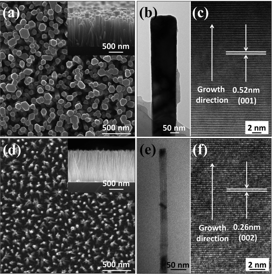 | ||
| Fig. 1 (a) Top view SEM, (b) TEM and (c) HRTEM images of Type A samples; (d) top view SEM, (e) TEM and (f) HRTEM images of Type B samples. Cross-sectional SEM images of the Type A and B samples are shown in the insets of (a) and (d), respectively. | ||
Fig. 2 presents SEM (a), (c) and TEM (b), (d) results for silica-coated Type A and B samples, respectively. Both samples retain their well-aligned nanorod morphology after the coating process; the individual nanorod diameters are obviously increased, but their lengths are little changed. The TEM image of a silica-coated Type A nanorod (Fig. 2(b)) reveals the expected core–shell structure, with a seemingly unchanged nanorod core encapsulated in a ∼13 nm thick silica shell. Fig. 2(d) indicates that silica coating a Type B nanorod is a less benign process: the interface between the silica shell and the ZnO core appears curved (as can be seen in the upper inset in Fig. 2(d)) and dark nanodots are clearly visible within the silica shell. HRTEM images of Type B samples (such as the one shown in the lower inset of Fig. 2(d)) allow estimation of the diameters of these nanodots (∼3–8 nm). Their composition is confirmed by the evident 0.26 nm interlayer spacing corresponding to the (002) planes of ZnO. These results imply that the silica coating process has significant impact on the morphology of the Type B nanorods, yet no obvious effect on Type A samples (apart from encapsulating them).
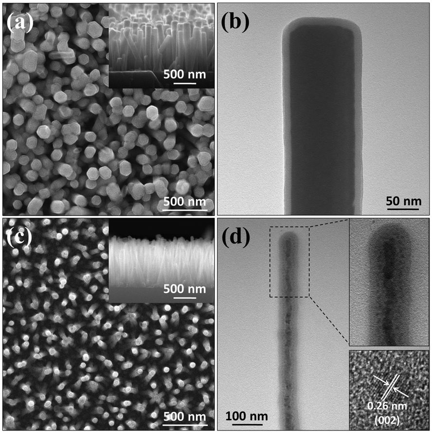 | ||
| Fig. 2 (a) Top view SEM and (b) TEM images of the silica-coated Type A sample; (c) top view SEM and (d) TEM images of the silica-coated Type B sample. The insets in (d) show, respectively, a × 2 enlarged view of the nanorod tip and a HRTEM image of an individual ZnO nanodot embedded within the silica shell. | ||
Fig. 3 shows PL spectra from bare Type A and Type B nanorod samples. Both show the characteristic sharp near band edge UV emissions at ∼388 nm and a broad visible emission centred at ∼575 nm. PL from ZnO samples excited at 325 nm, as here, is generally considered to emanate from penetration depths of up to 60–100 nm,23,24 and we thus assume that the present measurements sample the entire nanorod. Yellow emission around 570 nm in such PL spectra is traditionally attributed to oxygen-rich related bulk defects (e.g. oxygen interstitials) and/or to surface-related defects (e.g. adsorbed oxygen or water molecules);25–28 a range of other carriers (e.g. Zn vacancies, oxygen vacancies, oxide anti-sites, defect complexes, etc.) have been variously proposed to account for emissions appearing at blue, green and red wavelengths.28–33 Subjecting Type A and B nanorods to the exact same silica coating treatment results in strikingly different changes in the associated PL spectra. Type A nanorods show a substantially enhanced visible emission intensity (Ivis) and some modest increase in UV emission intensity (IUV) – as shown in Fig. 3(a) – whereas the Type B sample exhibits increased UV emission but its visible emission is little changed (Fig. 3(b)).
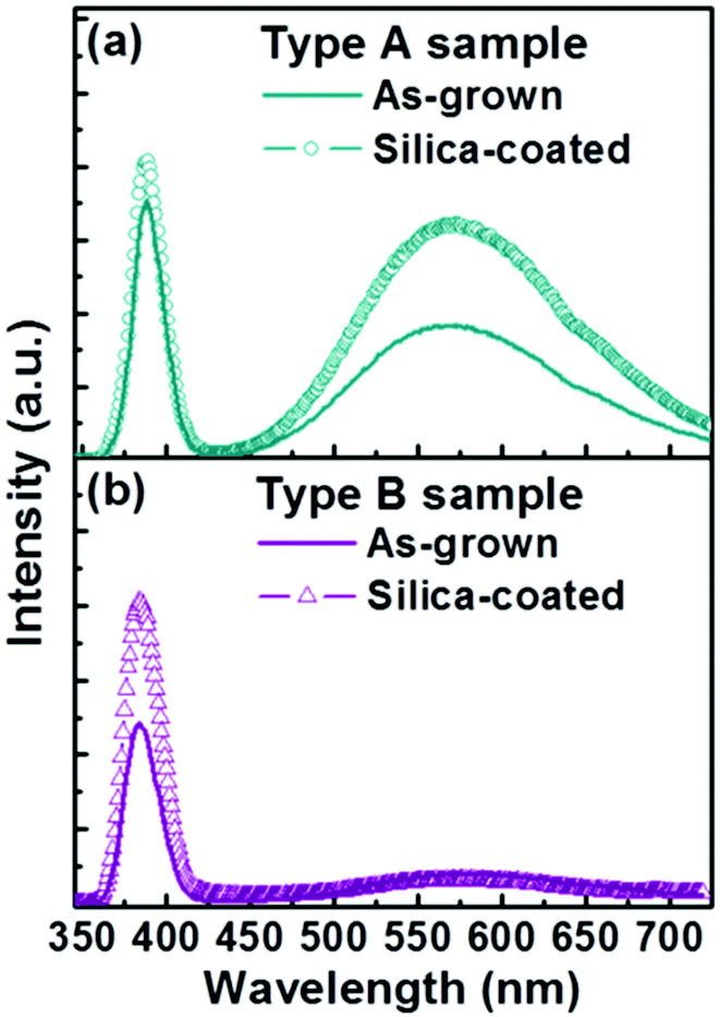 | ||
| Fig. 3 Typical PL spectra of (a) Type A and (b) Type B samples before and after the silica-coating process. | ||
Such seemingly contradictory findings have some resonance with several other reported studies of silica-coated ZnO nanomaterials34,35 and the remainder of this paper focusses on exploring why different ZnO nanorod samples, both synthesized by the same hydrothermal method, using the same reagents, and then silica coated under identical experimental conditions, lead to such different morphologies and PL properties. One obvious difference is the nanorod diameter: Type B nanorods are much thinner than Type A nanorods, and so present a much larger surface to volume ratio. But if the surface properties and the core structures of the two as-grown samples are the same, we might therefore expect that (1) the PL spectra of Type B nanorods would display smaller IUV/Ivis ratios than those of Type A nanorods, and (2) the respective nanorod morphologies and PL properties should change in similar ways when subjected to the same coating procedure. Neither expectation matches the current observations.
To investigate this further, the PL properties of bare Type A and Type B samples were compared before and after exposure to an Ar plasma (Fig. 4) and before and after annealing in Ar (Fig. 5). We start by noting that the as-grown Type B samples exhibit a much higher IUV/Ivis ratio. Neither post-treatment process had any discernible effect on the respective nanorod morphologies, but both had a significant impact on the PL spectrum. Plasma treatment results in decreased visible emission in both cases (down ∼25% in the case of Type A samples and by ∼75% for the Type B samples) and some modest increase in UV band emission (up ∼6% and ∼25% for Type A and Type B samples, respectively). Annealing in Ar has an even greater effect; the visible emission from the Type A (Type B) samples was reduced by ∼75% (∼90%), and the UV emissions increased by ∼17% (∼25%). Plasma treatment is traditionally viewed as the milder of these two post-processing techniques. Its role will be largely restricted to repairing surface defects and removing adsorbed surface species (e.g. oxygen or water molecules). Annealing in Ar can be expected both to ‘clean’ the surface and to reduce the bulk defect density (by annealing). The observed differences in the PL spectra of the two families of as-grown nanorod, and the different changes in PL spectra induced by these two post-treatments, all point to Type A samples having a substantially greater internal (bulk) defect density.
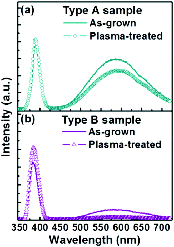 | ||
| Fig. 4 Typical PL spectra of (a) Type A and (b) Type B samples before and after Ar plasma treatment. | ||
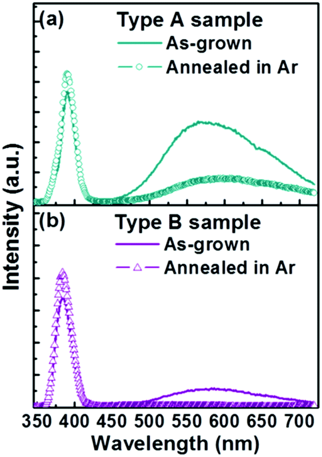 | ||
| Fig. 5 Typical PL spectra of (a) Type A and (b) Type B samples before and after annealing in Ar. | ||
The relative stability of the two as-grown samples in an alkaline environment was investigated also, by immersing each in a common mixture of 60 mL dehydrated ethanol and 3 mL ammonia for a period of 3 h (i.e. the same conditions as used for the silica coating process, but without any TEOS). As Fig. 6 shows, the PL spectrum of a Type A sample treated in this way is little changed from that of the as-grown sample, whereas exposing a Type B sample to the alkaline solution leads to a reduction in both the UV and visible emissions. The extent of this decrease scales with exposure time and, as Fig. 6 shows, is ∼60% after 3 h. This observed invariance (variance) in PL emission upon soaking Type A (B) samples in alkali solution has parallels with the observed invariance (variance) of the core of the Type A (B) nanorods during TEOS coating (recall Fig. 2(b) and (d)).
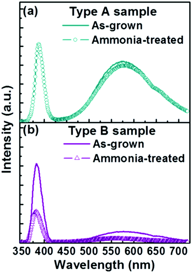 | ||
| Fig. 6 Typical PL spectra of (a) Type A and (b) Type B samples before and after the ammonia treatment. | ||
We have recently proposed22 that ZnO nanodot formation during TEOS treatment of thin ZnO nanorods (prepared using similar growth conditions (0.002 M concentrations of HMT and Zn(NO3)2) to those used when growing Type B nanorods in the present work) is facilitated by nanopores in the silica coating formed by hydrolysis and water condensation of TEOS.36,37 The presence of such nanopores allows reactive solution to reach the ZnO core and cause local dissolution. The dissolved material diffuses into the pores, nucleates and crystallizes as nanodots.
Why does the same dissolution/recrystallisation apparently not occur when TEOS treating a Type A sample? Why do Type A and Type B samples show different morphological behaviours and stabilities when immersed in an alkaline solution, and different defects and defect densities (as revealed by PL measurements on the various post-processed samples)? We suggest that the key is likely to be the different growth chemistry involved in forming the two sample types.
The kinetics of ZnO nanorod growth via the hydrothermal method used here has been investigated previously.38 The earlier study, which tracked not just the time dependent H+, Zn2+ and HMT concentrations but also the evolving morphology of the deposited ZnO material, concluded that the oxide precipitation mechanism is concentration dependent. Zn(OH)2 is a stable intermediate at high concentrations, but becomes thermodynamically unstable as the Zn2+ concentration declines.38,39 This has obvious parallels with the present work. Given the concentrations involved, growth of Type A samples will involve precipitation via the hydroxide, i.e.
| Zn2+ + 2OH− ⇌ Zn(OH)2 ⇌ ZnO + H2O | (1) |
| Zn2+ + 2OH− ⇌ ZnO + H2O | (2) |
It has been proposed previously that ZnO nanomaterials formed via different precipitation mechanisms could have different morphologies.38 The present study lends support to this view and implies that the crystallization (defects), the stability and the PL of ZnO nanorods are all sensitively dependent upon the precipitation mechanism. The work reported here suggests that crystallization via Zn(OH)2 intermediates yields Type A nanorods, with a high density of oxygen-rich bulk defects (as evidenced by the strong visible PL emission) and good stability with respect to basic (ammonia) solution. Type B nanorods, in contrast, formed by the direct reaction (2), have higher overall crystal quality (as evidenced by the strong UV and weak visible PL emissions) and greater reactivity towards ammonia.
The present observations broadly support the expectation that encapsulating ZnO in SiO2 leads to some passivation of the ZnO surface,40,41 reducing the electron depletion layer associated with the various surface defects in the as-grown material42–44 and enhancing the intensity of PL from the underlying ‘bulk’ material. Subjecting Type B nanorods to the TEOS-treatment clearly results in a substantial increase of the UV PL intensity (Fig. 3(b)), implying that the crystalline quality of the resulting ZnO nanodots (and the residual nanorod structures) is high and that SiO2 coating is indeed an effective route to surface passivation.23 Exposing Type B samples to an alkaline solution equivalent in all details apart from the absence of the TEOS, in contrast, leads to a uniform reduction in PL emission intensity (Fig. 6(b)), consistent with the evident reduction in the amount of ZnO material.
TEOS-treatment affects the PL spectrum of a Type A nanorod very differently – boosting the entire spectrum but particularly the visible component. After TEOS-treatment, most of this visible component must be attributable to sub-surface ‘bulk’ defects. Its increased showing can also be attributed to surface passivation by the SiO2 and the consequent reduction in depletion layer, but such an explanation does not account for the relatively greater boost to Ivis (cf. IUV). This difference could be understood if the penetration depth of the 325 nm light used in the present PL studies is considerably less than the 60–100 nm suggested in earlier studies23,24 and if oxygen-related defects (the assumed carrier of the visible emission) are preferentially partitioned near the surface. However, an alternative, and simpler, explanation recognizes that the absorption of the ZnO core and SiO2 coating is wavelength dependent, and higher in the near UV than in the visible.45,46 The silica coating can also attenuate PL from the ZnO core by internal reflection47 at the interfaces of core–shell structures. The ZnO core diameter in the Type A sample is comparable to the penetration length of the UV emission but much smaller than that of the visible emission. Thus we should expect relatively greater re-absorption of the UV component within the PL emanating from the core region. Re-absorption of the UV component within the PL emission has also been suggested as a route to promoting visible emission.48 All of the forgoing factors are likely to contribute to the observed boost of the visible component of the PL emission that results from SiO2 coating Type A ZnO nanorods. In passing, we note that we might also expect preferential re-absorption of the UV component of the PL from SiO2-coated Type B nanorods, but that any such effects will be much reduced by the small diameters of the ZnO nanorods and nanodots (cf. the penetration depth of the UV emission).
4. Conclusions
Two types of ZnO nanorod array, synthesized by the same hydrothermal method (using aqueous solutions but with different reagent concentrations) and then encapsulated in silica using an identical coating procedure, are shown to exhibit strikingly different PL properties and chemical stabilities. The source of these differences is traced to the different nanorod growth mechanisms. The thicker Type A samples, grown using high reagent concentrations, precipitate from Zn(OH)2. These give much stronger visible emission and are deduced to have a significantly higher density of bulk defects and to be more stable under the basic conditions of the silica coating process than the thinner Type B samples. The latter are grown from 20-times less concentrated reagent solutions. Zn(OH)2 is thermodynamically unstable under such conditions, and the nanorods form directly from successive reaction with Zn2+ and OH− ions at the growing (001) surface. The PL spectra of Type B nanorods are characterized by much higher IUV/Ivis ratios (implying that the bulk material is less defective), which can be improved further by SiO2 coating. These nanorods are less stable under the basic conditions prevailing during TEOS treatment, and much of the silica coated ZnO contributing to the measured PL spectra is in the form of nanodots. The present studies provide further fundamental insights into the controllable synthesis of ZnO nanomaterials and the possible modulation of their properties by silica coating, both of which could impact on future device applications and performance optimization.Acknowledgements
Financial support for this work was provided by the National Natural Science Foundation of China (grant no. 11104046), the National Basic Research Program of China (973 Program) (grant no. 2013CB632900), and by the Fundamental Research Funds for the Central University (grant no. HIT.BRETIII.201216, HIT.BRETIII.201225 and HIT.BRETIV.201313). M.Y. thanks the Young Thousand Plan for financial support.Notes and references
- Q. Yang, W. Wang, S. Xu and Z. L. Wang, Nano Lett., 2011, 11, 4012 CrossRef CAS PubMed.
- D. I. Son, B. W. Kwon, D. H. Park, W.-S. Seo, Y. Yi, B. Angadi, C. L. Lee and W. K. Choi, Nat. Nanotechnol., 2012, 7, 465 CrossRef CAS PubMed.
- S. Chu, G. Wang, W. Zhou, Y. Lin, L. Chernyak, J. Zhao, J. Kong, L. Li, J. Ren and J. Liu, Nat. Nanotechnol., 2011, 6, 506 CrossRef CAS PubMed.
- Q. Yang, Y. Liu, C. Pan, J. Chen, X. Wen and Z. L. Wang, Nano Lett., 2013, 13, 607 CrossRef CAS PubMed.
- X. Zhang, Y. Xia and T. He, Mater. Chem. Phys., 2012, 137, 622 CrossRef CAS PubMed.
- Y. Sun, N. G. Ndifor-Angwafor, D. J. Riley and M. N. R. Ashfold, Chem. Phys. Lett., 2006, 431, 352 CrossRef CAS PubMed.
- P. S. Venkatesh, S. Balakumar and K. Jeganathan, RSC Adv., 2014, 4, 5030 RSC.
- V. Chen, Y. Lu, H. He, M. Xiao, Z. Wang, L. Chen and Z. Ye, ACS Appl. Mater. Interfaces, 2013, 5, 10274 Search PubMed.
- R. Chen, Q. L. Ye, T. He, V. D. Ta, Y. Ying, Y. Y. Tay, T. Wu and H. Sun, Nano Lett., 2013, 13, 734 CrossRef CAS PubMed.
- C. W. Cheng, E. J. Sie, B. Liu, C. H. A. Huan, T. C. Sum, H. D. Sun and H. J. Fan, Appl. Phys. Lett., 2010, 96, 071107 CrossRef PubMed.
- Y. Lin, C. Xu, J. Li, G. Zhu, X. Xu, J. Dai and B. Wang, Adv. Opt. Mater., 2013, 1, 940 CrossRef.
- D. Zhao, X. Zhang, H. Dong, L. Yang, Q. Zeng, J. Li, L. Cai, X. Zhang, P. Luan, Q. Zhang, M. Tu, S. Wang, W. Zhou and S. Xie, Nanoscale, 2013, 5, 4443 RSC.
- C. Chen, H. He, Y. Lu, K. Wu and Z. Ye, ACS Appl. Mater. Interfaces, 2013, 5, 6354 CAS.
- M. Afsal, C. Y. Wang, L. W. Chu, H. Ouyang and L. J. Chen, J. Mater. Chem., 2012, 22, 8420 RSC.
- L. Wang, X. Zhang, Y. Fu, B. Li and Y. Liu, Langmuir, 2009, 25, 13619 CrossRef CAS PubMed.
- L. Wang, X. Zhang, B. Li, P. Sun, J. Yang, H. Xu and Y. Liu, ACS Appl. Mater. Interfaces, 2011, 3, 1277 CAS.
- J. Zhao, L. Wu and J. Zhi, J. Mater. Chem., 2008, 18, 2459 RSC.
- H. J. Zhang, H. M. Xiong, Q. J. Ren, Y. Y. Xia and J. L. Kong, J. Mater. Chem., 2012, 22, 13159 RSC.
- C. Y. Cho, N. Y. Kim, J. W. Kang, Y. C. Leem, S. H. Hong, W. Lim, S. T. Kim and S. J. Park, Appl. Phys. Express, 2013, 6, 042102 CrossRef.
- S. Panigrahi, A. Ber and D. Basak, J. Colloid Interface Sci., 2011, 353, 30 CrossRef CAS PubMed.
- B. H. Chu, L. C. Leu, C. Y. Chang, F. Lugo, D. Norton, T. Lele, B. Keselowsky, S. J. Pearton and F. Ren, Appl. Phys. Lett., 2008, 93, 233111 CrossRef PubMed.
- Y. Yin, Y. Sun, M. Yu, X. Liu, B. Yang, D. Liu, S. Liu, W. Cao and M. N. R. Ashfold, Nanoscale, 2014, 6, 10746 RSC.
- J. F. Muth, R. M. Kolbas, A. K. Sharma, S. Oktyabrsky and J. Narayan, J. Appl. Phys., 1999, 85, 7884 CrossRef CAS PubMed.
- J. F. Kong, H. Chen, H. B. Ye, W. Z. Shen, J. L. Zhao and X. M. Li, Appl. Phys. Lett., 2007, 90, 041907 CrossRef PubMed.
- S. Y. Liu, T. Chen, J. Wan, G. P. Ru, B. Z. Li and X. P. Qu, Appl. Phys. A, 2009, 94, 775 CrossRef CAS.
- Y. Sun, G. M. Fuge, N. A. Fox, D. J. Riley and M. N. R. Ashfold, Adv. Mater., 2005, 17, 2477 CrossRef CAS.
- A. B. Djurišić, Y. H. Leung, K. H. Tam, Y. F. Hsu, L. Ding, W. K. Ge, Y. C. Zhong, K. S. Wong, W. K. Chan, H. L. Tam, K. W. Cheah, W. M. Kwok and D. L. Phillips, Nanotechnology, 2007, 18, 095702 CrossRef.
- B. X. Lin, Z. X. Fu and Y. B. Jia, Appl. Phys. Lett., 2001, 79, 943 CrossRef CAS PubMed.
- H. Kaftelen, K. Ocakoglu, S. Tu, R. Thomann, S. Weber and E. Erdem, Phys. Rev. B: Condens. Matter, 2012, 86, 014113 CrossRef.
- A. Janotti and C. G. Van de Walle, Phys. Rev. B: Condens. Matter, 2007, 76, 165202 CrossRef.
- A. B. Djurisic, W. C. H. Choy, V. A. L. Roy, Y. H. Leung, C. Y. Kwong, K. W. Cheah, T. K. G. Rao, W. K. Chan, H. T. Lui and C. Surya, Adv. Funct. Mater., 2004, 14, 856 CrossRef CAS.
- A. Bera and D. Basak, Chem. Phys. Lett., 2009, 476, 262 CrossRef CAS PubMed.
- F. Fabbri, M. Villani, A. Catellani, A. Calzolari, G. Cicero, D. Calestani, G. Calestani, A. Zappettini, B. Dierre, T. Sekiguchi and G. Salviati, Sci. Rep., 2014, 4, 5158 CAS.
- S. Panigrahi and D. Basak, Chem. Phys. Lett., 2011, 511, 91 CrossRef CAS PubMed.
- N. Hagura, T. Takeuchi, S. Takayama, F. Iskandar and K. Okuyama, J. Lumin., 2011, 131, 138 CrossRef CAS PubMed.
- D. A. Firmansyah, S. G. Kim, K. S. Lee, R. Zahaf, Y. H. Kim and D. Lee, Langmuir, 2012, 28, 2890 CrossRef CAS PubMed.
- X. Zhang, C. Shao, Z. Zhang, J. Li, P. Zhang, M. Zhang, J. Mu, Z. Guo, P. Liang and Y. Liu, ACS Appl. Mater. Interfaces, 2012, 4, 4807 Search PubMed.
- M. N. R. Ashfold, R. P. Doherty, N. G. Ndifor-Angwafor, D. J. Riley and Y. Sun, Thin Solid Films, 2007, 515, 8679 CrossRef CAS PubMed.
- Y. Sun, D. J. Riley and M. N. R. Ashfold, J. Phys. Chem. B, 2006, 110, 15186 CrossRef CAS PubMed.
- K. S. Babu, A. R. Reddy and K. V. Reddy, Mater. Res. Bull., 2014, 49, 537 CrossRef CAS PubMed.
- P. K. Sharma, R. K. Dutta, M. Kumar, P. K. Singh and A. C. Pandey, J. Lumin., 2009, 129, 605 CrossRef CAS PubMed.
- C. M. Jin, A. Tiwari and R. J. Narayan, J. Appl. Phys., 2005, 98, 083707 CrossRef PubMed.
- X. L. Wu, G. G. Siu, C. L. Fu and H. C. Ong, Appl. Phys. Lett., 2001, 78, 2285 CrossRef CAS PubMed.
- Q. Zhang, J. Qi, Y. Huang, X. Li and Y. Zhang, Mater. Chem. Phys., 2011, 131, 258 CrossRef CAS PubMed.
- J. V. Foreman and H. O. Everitt, Phys. Rev. B: Condens. Matter, 2010, 81, 115318 CrossRef.
- H. R. Nikabadi, N. Shahtahmasebi, M. R. Rokn-Abadi, M. M. B. Mohagheghi and E. K. Goharshadi, Phys. Scr., 2013, 87, 025802 CrossRef.
- S. L. Chen, S. K. Lee, W. M. Chen, H. X. Dong, L. Sun, Z. H. Chen and I. A. Buyanova, Appl. Phys. Lett., 2010, 96, 033108 CrossRef PubMed.
- I. Hussain, N. Bano, S. Hussain, Y. Soomro, O. Nur and M. Willander, Materials, 2011, 4, 1260 CrossRef CAS PubMed.
| This journal is © the Partner Organisations 2015 |