
 Open Access Article
 This Open Access Article is licensed under a
 Creative Commons Attribution 3.0 Unported Licence
Direct imaging of boron segregation at dislocations in B:diamond heteroepitaxial films†
S.
Turner
*a,
H.
Idrissi
ab,
A. F.
Sartori
c,
S.
Korneychuck
a,
Y.-G.
Lu
ad,
J.
Verbeeck
a,
M.
Schreck
c and
G.
Van Tendeloo
a
aEMAT, University of Antwerp, Groenenborgerlaan 171, B-2020 Antwerp, Belgium. E-mail: stuart.turner@uantwerpen.be
bInstitute of Mechanics, Materials and Civil Engineering, Université catholique de Louvain, Place Sainte Barbe 2, B-1348 Louvain-la-Neuve, Belgium
cUniversität Augsburg, Institut für Physik, D-86135 Augsburg, Germany
dDepartment of Mechanical Engineering and Engineering Science, The University of North Carolina at Charlotte, 9201 University City Blvd., Charlotte, NC 28223, USA
First published on 21st December 2015
Abstract
A thin film of heavily B-doped diamond has been grown epitaxially by microwave plasma chemical vapor deposition on an undoped diamond layer, on top of a Ir/YSZ/Si(001) substrate stack, to study the boron segregation and boron environment at the dislocations present in the film. The density and nature of the dislocations were investigated by conventional and weak-beam dark-field transmission electron microscopy techniques, revealing the presence of two types of dislocations: edge and mixed-type 45° dislocations. The presence and distribution of B in the sample was studied using annular dark-field scanning transmission electron microscopy and spatially resolved electron energy-loss spectroscopy. Using these techniques, a segregation of B at the dislocations in the film is evidenced, which is shown to be intermittent along the dislocation. A single edge-type dislocation was selected to study the distribution of the boron surrounding the dislocation core. By imaging this defect at atomic resolution, the boron is revealed to segregate towards the tensile strain field surrounding the edge-type dislocations. An investigation of the fine structure of the B-K edge at the dislocation core shows that the boron is partially substitutionally incorporated into the diamond lattice and partially present in a lower coordination (sp2-like hybridization).
Introduction
Single crystal diamond is a material with extreme electrical and thermal properties which make it very desirable for high-end applications, such as radiation detection,1,2 electrochemical analysis,3 high power high frequency switching and rectifying,4 deep UV light emission,5etc. Many of these applications require controlled semiconducting properties, which nowadays are easily achievable in situ during microwave plasma chemical vapor deposition (MWPCVD) by adding boron or phosphorus precursors to the gas phase to promote, respectively, p-type or n-type conductivity by the substitutional incorporation of dopants into the diamond lattice. Boron is the most easily incorporated acceptor (p-type doping with a relatively low activation energy of 0.37 eV) and has therefore become the most widespread dopant for diamond.A promising route to synthesize single crystal diamond of a technologically relevant size (e.g. wafers) is heteroepitaxial deposition of diamond on iridium.6 This metal surface has turned out to be an ideal template for the generation of epitaxial diamond nuclei with unsurpassed areal density and alignment. During subsequent growth and coalescence, a closed diamond layer is formed after several tens of microns, giving rise to a diamond single crystal with a relatively high density of dislocations. Continuing CVD growth leads to an improved crystalline quality and a reduced density of dislocations down to the ∼107 cm−2 range, for a diamond thickness of ∼1 mm2. It is expected that the presence of such a high density of defects will strongly influence the charge carrier transport and presumably also the incorporation and distribution of the dopants into the diamond layers, as previously observed with other semiconductors.7–10 To properly understand the electrical properties of these types of boron-doped diamond films, knowledge of the concentration and distribution of the boron dopants inside the films is of fundamental importance.
For example, in recent work, the distribution of boron dopants in HPHT diamond was shown to have a significant influence on the superconducting properties of B:diamond.11,12 Earlier studies by our group have also shown that defects like twin boundaries and stacking faults in CVD grown boron doped diamond can be enriched in boron;13 a relaxation of the local lattice parameter at these defect sites enables the enrichment of boron.14 Knowing this behavior of boron from past experiments, the dislocation-rich nature of diamond single crystals heteroepitaxially grown on Ir/YSZ/Si(001) offers ideal conditions to study and understand the interaction between the dopant and the dislocations, which may provide further insights into growth, doping and dislocation propagation mechanisms that can have repercussions on material quality and ultimately on the device performance.
To this end, a thin film of heavily B-doped diamond was grown by MPCVD on an un-doped diamond layer grown on top of an Ir/YSZ/Si(001) substrate stack. In a first step, the density and nature of the dislocations in the film were investigated by conventional and weak-beam dark-field transmission electron microscopy (WBDF TEM) techniques. After characterization of the dislocations in the film, the presence and distribution of B in the sample was studied using a combination of annular dark-field (high resolution) scanning transmission electron microscopy ((HR)ADF-STEM) and spatially resolved electron energy-loss spectroscopy (STEM-EELS), performed on a state-of-the-art aberration corrected TEM instrument. As described above, this technique was previously used with success to map out the boron distribution around defects in CVD grown nanocrystalline diamond. In this manner here, the B concentration, distribution and the local B environment in this type of dislocation-rich diamond hetero-epitaxial film could be determined. Finally, by performing these types of STEM-EELS experiments in plan-view, and at a high resolution, the relationship between the strain field of the dislocations present in the sample and boron enrichment was investigated.
Experimental
Sample growth
The diamond samples were grown by MWPCVD in two steps on top of a Ir/YSZ/Si(001) substrate with an off-axis angle of 6° along the [110] direction. The first step consisted of growing a ∼1 mm thick diamond (the first half with N2 added to the gas phase and the second half without). Next, the diamond sample had its Ir/YSZ/Si(001) substrate removed and the dislocation-rich backside was mechanically polished (several tens of microns of diamond were removed), followed by cleaning in hydrogen plasma. Subsequently, a 1–2 μm thick heavily B-doped layer was grown by MPCVD on this side of the diamond, with the addition of 980 ppm trimethylborane (TMB) to the gas phase and 2% CH4 ([B/C]gas = 42![[thin space (1/6-em)]](https://www.rsc.org/images/entities/char_2009.gif) 763 ppm). The backside was chosen as the growth substrate for the B-doping process in order to guarantee a higher number of dislocations in the electron transmittable area of the TEM samples. Finally, a plasma etching step was carried out to produce etch pits on the diamond surface.
763 ppm). The backside was chosen as the growth substrate for the B-doping process in order to guarantee a higher number of dislocations in the electron transmittable area of the TEM samples. Finally, a plasma etching step was carried out to produce etch pits on the diamond surface.
The preparation of the Ir/YSZ/Si(001) substrate and diamond nucleation by bias-enhanced nucleation (BEN) is described in detail elsewhere.15 In short, a several 10s of nms thick layer of yttria-stabilized zirconia (YSZ) was deposited epitaxially on the Si(001) substrate by pulsed laser deposition (PLD),16 followed by an e-beam evaporation of Ir.17 The resulting Ir single crystal film enabled the BEN step to produce the highly oriented diamond nuclei, which was followed by a short MWPCVD growth step to close the diamond film before further growth steps are carried out.
Sample preparation and TEM experiments
The samples for TEM investigation were prepared by using a focused ion beam lift-out procedure, carried out in a FEI Helios FIB/SEM instrument. In order to view the etch pits in plan-view, the samples were cut relatively close to the film surface. To study single dislocation in plan-view (Fig. 4 and 5), FIB plan-view slices were taken deeper into the B:diamond film (approximately 500 nm into the film).Bright field (BF) and WBDF TEM images were acquired on a FEI Tecnai microscope, operated at 200 kV. Aberration-corrected high resolution TEM imaging was performed on a FEI Titan “cubed” microscope, operated at a 300 kV acceleration voltage and equipped with both TEM and STEM aberration correctors. Aberration-corrected TEM imaging was performed under negative Cs conditions (Cs tuned to −12 μm). Aberration-corrected ADF-STEM imaging was performed on the same microscope, operated at a 300 kV acceleration voltage. The convergence semi-angle α was 21 mrad, the ADF inner acceptance angle β and the EELS acceptance angle were both 28 mrad. Quantification of the boron content was performed using the Gatan Digital Micrograph (DM) software package, using Hartree–Slater cross sections. Fourier filtering of the high resolution images was performed by masking the lattice reflections in a Fourier transform pattern and back-transforming to yield the filtered image. This filtering was also performed using the digital micrograph (DM) software package.
Results and discussion
Fig. 1a–c show an overview of the B:diamond samples grown for investigation by microwave plasma CVD. The boron-doped diamond thin films were grown on a Ir/YSZ/Si(001) stack. In order to systematically study the dislocations present in the samples, focussed ion beam lift out sample preparation procedures were adopted to prepare TEM specimens in both cross-sectional and plan-view orientations (Fig. 1d).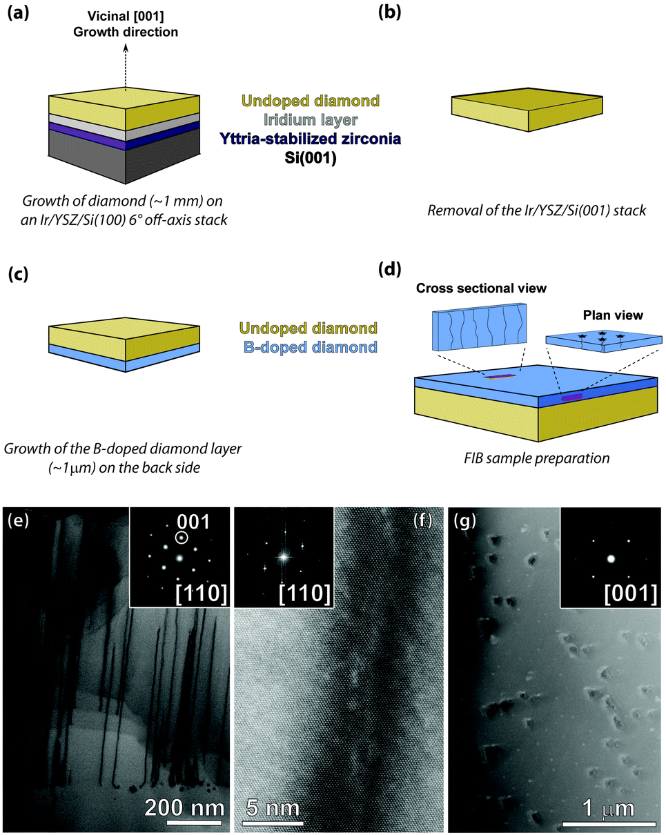 | ||
| Fig. 1 Overview of the B:diamond samples. (a–d) Sample growth steps and FIB preparation geometries. Diagram showing the plan-view and cross-sectional FIB preparation geometries. (e) Overview CS TEM image showing the dislocations in the film. (f) HR ADF-STEM CS image of a single dislocation along the [110] zone axis. (g) Overview PV TEM image, showing triangular etch pits at the film surface. | ||
An overview BF-TEM image of the diamond thin film is displayed in Fig. 1e. The accompanying diffraction pattern (inset) confirms that the thin film is monocrystalline diamond, being viewed along the [110] zone axis orientation, with the diamond/B:diamond interface being close to the (001) plane. In fact, the diffraction pattern demonstrates that, as a result of the 6 degree off-cut, the [001] growth direction of the diamond film is slightly tilted with respect to the diamond/B:diamond interface by approximately 8 degrees. The dislocations present in the film appear as dark-contrast lines in this BF TEM image. The visibly parallel dislocation lines follow the [001] growth direction of the film, and usually thread through the entire film thickness, having originated at the diamond/B:diamond interface.18 In (f), a bright field high resolution scanning transmission electron microscopy image of a single dislocation in cross-section is shown. From the image, it is clear that at an atomic level the dislocation is not straight, but rather displays a local wavy nature, while retaining a global [001] growth direction. Fig. 1g is a plan-view overview image of a dislocation-rich sample. Etch-pit structures are visible throughout the sample, with each pit marking the position of a single dislocation or bundle of dislocations in the diamond thin film.
In order to study the nature of the dislocations present in the boron doped diamond film, we adopted the weak-beam dark-field TEM technique. Using this technique, the Burgers vector of dislocations can be identified based on the invisibility criteria  . Furthermore, the near-core properties of the dislocations can be revealed. Typically, dislocations in CVD diamond lie along <100> and have Burgers vectors
  . Both mixed-type and pure edge dislocations have been reported in the literature.19 In the present study, the extinction conditions (all details and acquired dark-field images are presented in the ESI†) pointed out that both edge and mixed 45° type [001] dislocations are present in the B:diamond film. An example of edge and 45° dislocations is shown in the WBDF images of Fig. 2a and b obtained with g =
 ![[2 with combining macron]](https://www.rsc.org/images/entities/char_0032_0304.gif) 20 and g = 004 respectively, in a [110] oriented FIB foil. Some dislocations are decorated by loops, which are particularly visible in the WBDF image of Fig. 2b. In most cases the loops exhibit a diffraction contrast parallel to the projection of the trace of the {111} planes of the diamond lattice, like the example shown in the image of Fig. 2c. Note that the image of Fig. 2c was obtained in a [010] oriented FIB foil. A second peculiarity of the dislocations is the interrupted contrast at high magnification. As can be seen in the WBDF image of Fig. 2d obtained in the [110] oriented FIB foil, both edge and 45° mixed dislocation lines do not display a solid, uninterrupted diffraction contrast, but rather an intermittent one, which might point in the direction of clustered segregation of boron at the dislocations. The presence of edge and mixed 45° type [001] dislocations is in excellent agreement with the work by Gaukroger et al. on homoepitaxial diamond samples grown by MP-CVD.19 The dislocation density measured in the WBDF images was around 2 × 1010 cm−2.
20 and g = 004 respectively, in a [110] oriented FIB foil. Some dislocations are decorated by loops, which are particularly visible in the WBDF image of Fig. 2b. In most cases the loops exhibit a diffraction contrast parallel to the projection of the trace of the {111} planes of the diamond lattice, like the example shown in the image of Fig. 2c. Note that the image of Fig. 2c was obtained in a [010] oriented FIB foil. A second peculiarity of the dislocations is the interrupted contrast at high magnification. As can be seen in the WBDF image of Fig. 2d obtained in the [110] oriented FIB foil, both edge and 45° mixed dislocation lines do not display a solid, uninterrupted diffraction contrast, but rather an intermittent one, which might point in the direction of clustered segregation of boron at the dislocations. The presence of edge and mixed 45° type [001] dislocations is in excellent agreement with the work by Gaukroger et al. on homoepitaxial diamond samples grown by MP-CVD.19 The dislocation density measured in the WBDF images was around 2 × 1010 cm−2.
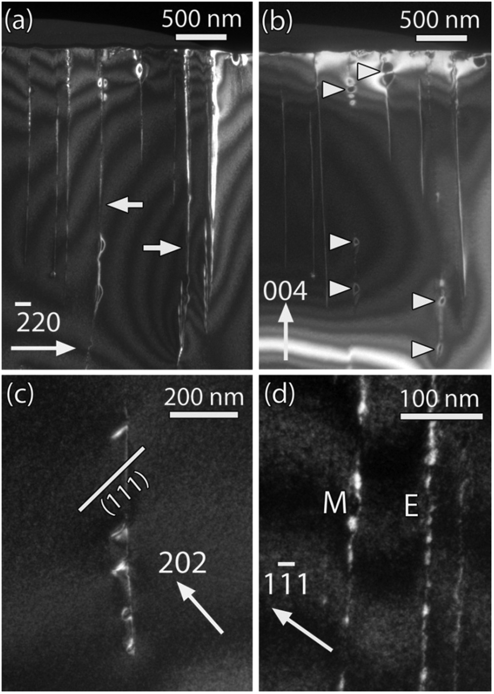 | ||
Fig. 2 Characterisation of the [001] dislocations using weak-beam dark-field TEM. (a) and (b) WBDF images obtained with g = 20 and g = 004, respectively. Edge dislocations with  are marked by white arrows in (a). They are invisible with g = 004. The dislocations which are visible in (a) and (b) are 45° mixed dislocations (see the ESI†). Note the presence of loops (white arrowheads) on both edge and 45° dislocations in (b). (c) g = 202 image showing loops parallel to the projection of the trace of the (111) plane. This projection is indicated by a solid white line. (d) g = 1 are marked by white arrows in (a). They are invisible with g = 004. The dislocations which are visible in (a) and (b) are 45° mixed dislocations (see the ESI†). Note the presence of loops (white arrowheads) on both edge and 45° dislocations in (b). (c) g = 202 image showing loops parallel to the projection of the trace of the (111) plane. This projection is indicated by a solid white line. (d) g = 1![[1 with combining macron]](https://www.rsc.org/images/entities/char_0031_0304.gif) 1 image showing interrupted diffraction contrast on edge ‘E’ and 45° mixed ‘M’ dislocations. 1 image showing interrupted diffraction contrast on edge ‘E’ and 45° mixed ‘M’ dislocations. | ||
In order to measure the distribution of boron within the B:diamond film, we adopted a combination of scanning transmission electron microscopy and electron energy-loss spectroscopy. In the first experiment, a single dislocation was scanned using spatially resolved EELS. In this technique, the fine electron probe is scanned over the sample, acquiring an EELS spectrum at every scan point. Each acquired spectrum contained both the boron-K and carbon-K EELS edges. An ADF-STEM overview image of the studied dislocation is shown in Fig. 3a. A typical EELS spectrum acquired from the sample is plotted in Fig. 3f. Upon a first inspection, it is clear that two edges are present in the EELS spectrum: a weak boron K-edge around 190 eV, and a strong carbon K-edge at 285 eV. The fine structure of the carbon K-edge is typical of diamond, with a large σ* contribution at 292 eV, and a small π* contribution at 285 eV. The origin of the π* contribution is likely to be twofold: on the one hand, surface amorphization of the sample has surely occurred during sample preparation. On the other hand, it can be expected that the carbon atoms close to the dislocations show a larger π* contribution due to the presence of distorted and/or dangling bonds at defects.13,14 The boron edge at 190 eV shows the presence of three distinct sub-peaks. These sub-peaks A, B and C are typical signatures for tetrahedrally embedded boron in diamond, and will be discussed further below.
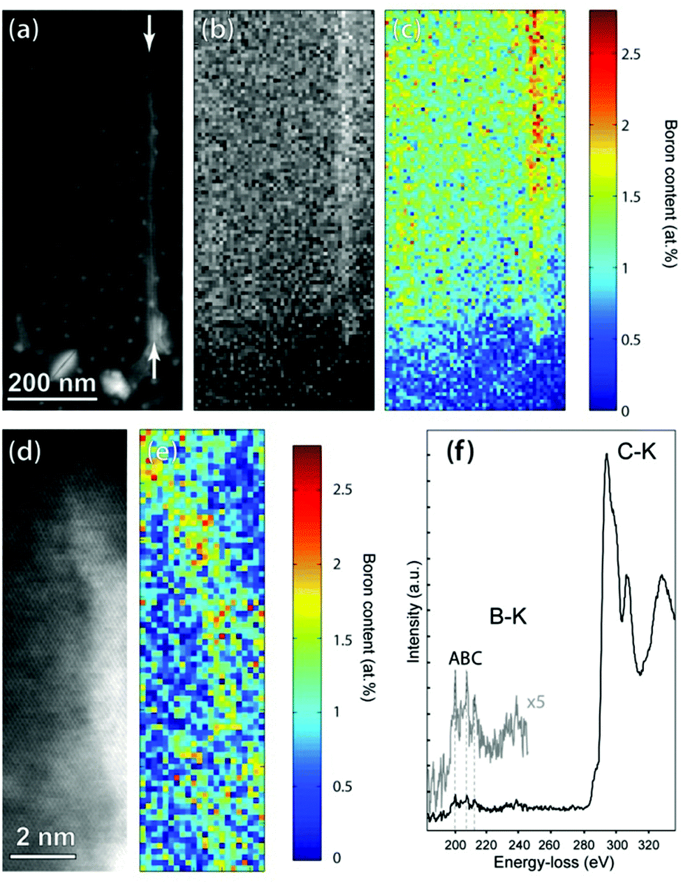 | ||
| Fig. 3 Detection of B using EELS. (a) Overview ADF-STEM image showing a single dislocation (arrows). (b) Boron K-edge map, showing boron segregation at the dislocation. (c) Boron content map, showing that the boron content in the dislocation can reach up to 2.5 at%. (d) HR ADF-STEM image of a single dislocation. (e) Boron content map. The width of the B enriched region is approximately 2 nm. (f) EELS spectrum from a pristine diamond area, showing the B-K edge at 190 eV and the C-K edge at 285 eV. | ||
By plotting the integrated intensity under the boron-K edge, a quantitative boron map can be calculated. This map, displayed in Fig. 3c, clearly shows that even though a boron signal is measured within the whole B:diamond film, an enrichment of boron is present at the dislocation. The measured background signal of boron in a film of 1.0–1.5 at% (1.8–2.7 × 1021 cm−3) is in good correspondence with the nominal boron content, derived from the process gas composition in combination with former results on the incorporation efficiency under these process conditions. At the dislocation, the boron signal rises to approximately 2.5 at% (4.4 1021 × cm−3). These numbers must of course be interpreted with due caution; the single dislocation does not fill the full sample thickness, meaning the real “local” concentration of boron in the dislocation is expected to be significantly higher than the measured 2.5 at%. The fact that a clear enrichment of boron is observed in the dislocations is in agreement with the observation of loops by WBDF, decorating the dislocation lines (see Fig. 2c), which are expected to be boron rich. A STEM-EELS scan performed at a higher resolution, presented in Fig. 3d and e, shows similar results; the projected boron to carbon ratio along the dislocation can reach up to 2.5 at%. The width of the boron-rich dislocation region is approximately 2 nm, which is in good agreement with the strain field visualised in Fig. 1f. Interestingly, the high resolution scan confirms the trend seen in the dark-field images; the boron enrichment along the dislocation line is not constant, but rather intermittent in nature.
A detailed high resolution investigation of the two types of dislocations present in the sample is provided in Fig. 4. Fig. 4a and d are aberration-corrected HRTEM images of single edge-type and 45° mixed-type dislocations, respectively, viewed along the [001] zone axis (in plan-view). These images were taken under so-called negative Cs imaging conditions (Cs was set to −12 μm). Under these conditions, an enhanced contrast can be achieved for light elements, by balancing a positive defocus with a negative spherical aberration coefficient.20 Indeed, HRTEM image simulations indicate that under the slight overfocus conditions used for imaging (close to the optimal Scherzer defocus of +6 nm), the carbon atomic columns in the structure are imaged as white contrast on a dark background. Knowing the contrast transfer of the microscope through image simulations allows us to indicate the positions of the atomic columns in images 4a and d. In order to visualize the core of the dislocation more clearly, the image was Fourier-filtered, and the filtered image is presented in Fig. 4b and e. The edge dislocation clearly consists of a single extra {110}-type half-plane, inserted from the top of the image. The structure of the core strongly resembles the zigzagged <100> edge-type dislocation core, as presented by Fujita et al.21 The strain field surrounding the dislocation can be mapped out using the so-called geometrical phase analysis (GPA) approach. In this method, developed by Hÿtch et al., variations in inter-atomic distances can be mapped out in a quantitative manner.22 The GPA corresponding to the edge dislocation is displayed in Fig. 4c. It is important to note that this GPA treatment was performed on raw data, and not on the Fourier filtered data. In Fig. 4c, the strain was defined with respect to the bulk region away from the dislocation core, where the strain is assumed to be zero. The magnitude of strain εxx is shown on the colour scale. The origin of the x-axis and y-axis was set at the core of the dislocation. It is clear from the image that the diamond lattice is strained in a compressive manner on the side of the extra {110}-type half plane, while the lattice undergoes tensile stress on the other side.
 | ||
| Fig. 4 High resolution characterisation of the dislocations in the B:diamond film. (a) HRTEM image of an edge dislocation. (b) Fourier-filtered image of the dislocation core. The white dots indicate the atom column positions (c) GPA map of the edge dislocation, showing the strain field surrounding the core. Color indicates the strain εxx (d) HRTEM image of a mixed-type dislocation. (e) Fourier-filtered image of the dislocation core. The white dots indicate the atom column positions (f) GPA map of the mixed-type dislocation, showing the strain field surrounding the core. Note the slight distortion of the strain field of the dislocation in (f) due to the presence of neighbouring dislocations. The origin of x-axis and y-axis was set at the core of the dislocations. | ||
The second type of dislocation found in the film is the mixed 45°-type dislocation. A high resolution image of such a dislocation is displayed in Fig. 4d. This dislocation type differs significantly from the edge type dislocation described above. In this case, the dislocation shows the insertion of two, not one, {110} type half-planes into the structure, that meet at the dislocation core under a 90 degree angle. The structure of the dislocation core becomes most apparent after Fourier filtering, as shown in Fig. 4e. To the best of our knowledge, this is the first, direct visualisation of a mixed-type dislocation in diamond. The structure of the core coincides well with the literature model, predicted using density functional theory.23 The tensile and compressive strain fields surrounding the core of the 45°-type dislocation are shown in the GPA map of Fig. 4f.
In the final experiment, a single edge-type dislocation was investigated using spatially resolved EELS, in an attempt to precisely localise the boron with respect to the dislocation core. An edge-type dislocation was selected, as this type of dislocation appeared to be more stable under electron irradiation than the mixed-type dislocation. Fig. 5a is an aberration-corrected ADF-STEM image of a single edge-type dislocation in plan-view (along the [001] zone axis orientation). The Fourier-filtered image in Fig. 5b clearly demonstrates the insertion of an extra {110}-type half plane into the diamond lattice, from the right of the image. After ADF-STEM imaging, the region indicated by the white rectangle in Fig. 5a was scanned using the same fine electron probe, acquiring an EELS spectrum containing both the boron-K and the carbon-K edge and an additional ADF-STEM image simultaneously. This simultaneous acquisition of an atomic resolution ADF-STEM image allows us to exactly pinpoint the position of the dislocation with respect to the acquired EELS data. In Fig. 5c, the boron distribution surrounding the dislocation is mapped out. The boron is clearly enriched close to the dislocation core, as was to be expected from the cross-sectional experiments. Intriguingly, the boron is not distributed symmetrically around the dislocation. This is visible from the colour overlay of the boron signal (in green) on top of the simultaneously acquired ADF-STEM data (in purple) in Fig. 5d. The dislocation core is marked by a white “T” in the image. It is clear from the data that rather than a symmetrical boron distribution around the dislocation core, the boron is enriched on the side of the dislocation that is under tensile strain. This boron distribution is not unexpected: the tensile strain makes extra room to embed boron either substitutionally or interstitially into the diamond lattice. Furthermore, a similar dopant enrichment of In in InGaN was recently confirmed using spatially resolved EDX by Horton et al.24
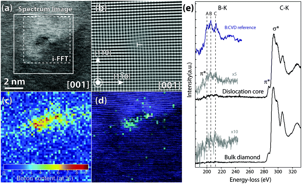 | ||
| Fig. 5 Spectroscopic investigation of a single edge-type dislocation. (a) Overview ADF-STEM image of a single edge dislocation. (b) Fourier filtered image of the dislocation core, showing the insertion of an extra half-plane. The white T marks the exact position of the edge dislocation. (c) Boron content map, showing the enrichment of B close to the dislocation core. (d) False-colour image of the plotted B signal on top of the simultaneously acquired HAADF-STEM image. The white T marks the exact position of the edge dislocation. The boron segregates to area of tensile stress surrounding the dislocation. (e) EELS spectra containing the B-K and C-K edges. The boron signal in the dislocation core is clearly higher than in the bulk. A fine structure reference for tetrahedrally embedded boron in diamond is plotted in blue. | ||
Interesting information can be derived from the fine structure of the boron K-edge at the dislocation core. The boron and carbon K-edges averaged over the dislocation core, together with data averaged over a pristine region of the B:diamond film, are plotted in Fig. 5e. A fine structure reference from tetrahedrally (substitutionally) embedded boron in diamond is plotted in blue. This reference, showing the presence of three typical sub-peaks A, B and C, has previously been measured in both CVD and HPHT B-doped diamond, and was simulated using density functional theory, in order to prove that it corresponds to the substitutionally embedded boron in diamond.12,25,26 The data acquired from the dislocation core show the presence of these three sub-peaks, confirming that at least part of the boron close to the core of the dislocation is embedded tetrahedrally. However, a clear π* contribution is also measured at 194 eV, indicating that a significant amount of the boron close to the dislocation is present in a lower coordination. This heightened π* contribution was previously observed by EELS at twin boundaries and grain boundaries, and is most likely due to a heightened presence of dangling and distorted bonds there.
Conclusions
In this work, a thin film of heavily B-doped diamond has been grown by MPCVD on an un-doped diamond layer, on top of an Ir/YSZ/Si(001) substrate stack. In the first step, the density and nature of the dislocations in the film were investigated by conventional and weak-beam dark-field transmission electron microscopy techniques. After characterization of the dislocations in the film, the presence and distribution of B in the sample was studied using a combination of annular dark-field scanning transmission electron microscopy and spatially resolved electron energy-loss spectroscopy, performed on a state-of-the-art aberration corrected TEM instrument. Using these tools, the B concentration, distribution and the local B environment in this type of dislocation-rich diamond hetero-epitaxial film has been determined, as performed previously for the polycrystalline B:diamond material from CVD growth. A specific enrichment of B at dislocations is evidenced, which is shown not to be uniform, but intermittent along the dislocation line. An investigation of a single edge-type dislocation revealed a segregation of boron towards the tensile strain field surrounding the edge-type dislocations. The fine structure of the B-K edge at the dislocation core showed that boron is partially substitutionally incorporated into the diamond lattice, and partially present in a lower coordination (sp2-like hybridization).Acknowledgements
The authors gratefully acknowledge Prof. Dominique Schryvers for fruitful discussions. S. T. acknowledges the fund for scientific research Flanders (FWO) for a post-doctoral scholarship and under contract number G.0044.13N. The Augsburg team acknowledges Dr Martin Fischer and Dr Stefan Gsell for kindly preparing and supplying the diamond/Ir/YSZ/Si(001) substrates used in this work, as well as the funding support from the European Community's Seven Framework Program (FP7/2009–2013, Marie Curie ITN) under grant agreement 238201. HI acknowledges the IAP program of the Belgian State Federal Office for Scientific, Technical and Cultural Affairs, under Contract No. P7/21 and the m.era – FASS project. The microscope used for this study was partly funded by the Hercules fund from the Flemish Government.Notes and references
- M. Pimpinella, I. Ciancaglioni, R. Consorti, C. Di Venanzio, A. S. Guerra, A. Petrucci, A. Stravato and G. Verona-Rinati, Metrologia, 2012, 49, S207–S210 CrossRef CAS.
- C. Stehl, M. Fischer, S. Gsell, E. Berdermann, M. S. Rahman, M. Traeger, O. Klein and M. Schreck, Appl. Phys. Lett., 2013, 103 Search PubMed.
- Y. Einaga, J. S. Foord and G. M. Swain, MRS Bull., 2014, 39, 525–532 CrossRef CAS.
- S. Yamasaki, E. Gheeraert and Y. Koide, MRS Bull., 2014, 39, 499–503 CrossRef CAS.
- T. Makino, K. Yoshino, N. Sakai, K. Uchida, S. Koizumi, H. Kato, D. Takeuchi, M. Ogura, K. Oyama, T. Matsumoto, H. Okushi and S. Yamasaki, Appl. Phys. Lett., 2011, 99 Search PubMed.
- M. Schreck, J. Asmussen, S. Shikata, J.-C. Arnault and N. Fujimori, MRS Bull., 2014, 39, 504–510 CrossRef CAS.
- S. Hashimoto, Y. Yoshizumi, T. Tanabe and M. Kiyama, J. Cryst. Growth, 2007, 298, 871–874 CrossRef CAS.
- L. McCarthy, I. Smorchkova, H. Xing, P. Fini, S. Keller, J. Speck, S. P. DenBaars, M. J. W. Rodwell and U. K. Mishra, Appl. Phys. Lett., 2001, 78, 2235–2237 CrossRef CAS.
- H. Idrissi, G. Regula, M. Lancin, J. Douin and B. Pichaud, Phys. Status Solidi C, 2005, 2, 1998–2003 CrossRef CAS.
- H. Idrissi, B. Pichaud, G. Regula and M. Lancin, J. Appl. Phys., 2007, 101, 113533 CrossRef.
- G. Zhang, S. Turner, E. A. Ekimov, J. Vanacken, M. Timmermans, T. Samuely, V. A. Sidorov, S. M. Stishov, Y. Lu, B. Deloof, B. Goderis, G. Van Tendeloo, J. Van de Vondel and V. V. Moshchalkov, Adv. Mater., 2014, 26, 2034–2040 CrossRef CAS PubMed.
- Y.-G. Lu, S. Turner, E. A. Ekimov, J. Verbeeck and G. Van Tendeloo, Carbon, 2015, 86, 156–162 CrossRef CAS.
- Y.-G. Lu, S. Turner, J. Verbeeck, S. D. Janssens, P. Wagner, K. Haenen and G. Van Tendeloo, Appl. Phys. Lett., 2012, 101 Search PubMed.
- Y.-G. Lu, S. Turner, J. Verbeeck, S. D. Janssens, K. Haenen and G. Van Tendeloo, Appl. Phys. Lett., 2013, 103 Search PubMed.
- M. Fischer, S. Gsell, M. Schreck, R. Brescia and B. Stritzker, Diamond Relat. Mater., 2008, 17, 1035–1038 CrossRef CAS.
- S. Gsell, M. Fischer, T. Bauer, M. Schreck and B. Stritzker, Diamond Relat. Mater., 2006, 15, 479–485 CrossRef CAS.
- S. Gsell, M. Fischer, M. Schreck and B. Stritzker, J. Cryst. Growth, 2009, 311, 3731–3736 CrossRef CAS.
- P. M. Martineau, S. C. Lawson, A. J. Taylor, S. J. Quinn, D. J. F. Evans and M. J. Crowder, Gems Gemol., 2004, 40, 2–25 CrossRef CAS.
- M. P. Gaukroger, P. M. Martineau, M. J. Crowder, I. Friel, S. D. Williams and D. J. Twitchen, Diamond Relat. Mater., 2008, 17, 262–269 CrossRef CAS.
- C. L. Jia, M. Lentzen and K. Urban, Science, 2003, 299, 870–873 CrossRef CAS PubMed.
- N. Fujita, A. T. Blumenau, R. Jones, S. Oberg and P. R. Briddon, Phys. Status Solidi A, 2007, 204, 2211–2215 CrossRef CAS.
- M. J. Hÿtch, E. Snoeck and R. Kilaas, Ultramicroscopy, 1998, 74, 131–146 CrossRef.
- N. Fujita, A. T. Blumenau, R. Jones, S. Oberg and P. R. Briddon, Phys. Status Solidi A, 2006, 203, 3070–3075 CrossRef CAS.
- M. K. Horton, S. Rhode, S.-L. Sahonta, M. J. Kappers, S. J. Haigh, T. J. Pennycook, C. J. Humphreys, R. O. Dusane and M. A. Moram, Nano Lett., 2015, 15, 923–930 CrossRef CAS PubMed.
- S. Turner, Y.-G. Lu, S. D. Janssens, F. Da Pieve, D. Lamoen, J. Verbeeck, K. Haenen, P. Wagner and G. Van Tendeloo, Nanoscale, 2012, 4, 5960–5964 RSC.
- S. Heyer, W. Janssen, S. Turner, Y.-G. Lu, W. S. Yeap, J. Verbeeck, K. Haenen and A. Krueger, ACS Nano, 2014, 8, 5757–5764 CrossRef CAS PubMed.
Footnote |
| † Electronic supplementary information (ESI) available. See DOI: 10.1039/c5nr07535a |
| This journal is © The Royal Society of Chemistry 2016 |