
 Open Access Article
 This Open Access Article is licensed under a
 Creative Commons Attribution 3.0 Unported Licence
2D nanosheet molybdenum disulphide (MoS2) modified electrodes explored towards the hydrogen evolution reaction†
Samuel J.
Rowley-Neale
a,
Dale A. C.
Brownson
a,
Graham C.
Smith
b,
David A. G.
Sawtell
a,
Peter J.
Kelly
a and
Craig E.
Banks
*a
aFaculty of Science and Engineering, School of Science and the Environment, Division of Chemistry and Environmental Science, Manchester Metropolitan University, Chester Street, Manchester M1 5GD, UK. E-mail: c.banks@mmu.ac.uk; Web: http://www.craigbanksresearch.com Fax: +(0)1612476831; Tel: +(0)1612471196
bFaculty of Science and Engineering, Department of Natural Sciences, University of Chester, Thornton Science Park, Pool Lane, Ince, Chester CH2 4NU, UK
First published on 6th October 2015
Abstract
We explore the use of two-dimensional (2D) MoS2 nanosheets as an electrocatalyst for the Hydrogen Evolution Reaction (HER). Using four commonly employed commercially available carbon based electrode support materials, namely edge plane pyrolytic graphite (EPPG), glassy carbon (GC), boron-doped diamond (BDD) and screen-printed graphite electrodes (SPE), we critically evaluate the reported electrocatalytic performance of unmodified and MoS2 modified electrodes towards the HER. Surprisingly, current literature focuses almost exclusively on the use of GC as an underlying support electrode upon which HER materials are immobilised. 2D MoS2 nanosheet modified electrodes are found to exhibit a coverage dependant electrocatalytic effect towards the HER. Modification of the supporting electrode surface with an optimal mass of 2D MoS2 nanosheets results in a lowering of the HER onset potential by ca. 0.33, 0.57, 0.29 and 0.31 V at EPPG, GC, SPE and BDD electrodes compared to their unmodified counterparts respectively. The lowering of the HER onset potential is associated with each supporting electrode's individual electron transfer kinetics/properties and is thus distinct. The effect of MoS2 coverage is also explored. We reveal that its ability to catalyse the HER is dependent on the mass deposited until a critical mass of 2D MoS2 nanosheets is achieved, after which its electrocatalytic benefits and/or surface stability curtail. The active surface site density and turn over frequency for the 2D MoS2 nanosheets is determined, characterised and found to be dependent on both the coverage of 2D MoS2 nanosheets and the underlying/supporting substrate. This work is essential for those designing, fabricating and consequently electrochemically testing 2D nanosheet materials for the HER.
1. Introduction
The increasing scarcity of fossil fuels coupled with the consequences of anthropogenic climate change has produced a global need to find feasible alternatives to energy generation.1–3 One scenario of change is creating a global hydrogen economy in which energy generation demands are met partially or entirely by hydrogen fuel cells.4–6 Utilising hydrogen fuels in this manner would cause a dramatic decrease in the anthropogenic greenhouse emissions and ozone precursors released by fossil fuel combustion given that the major product of hydrogen oxidation is H2O.4,7 The main barrier to the implementation of such a hydrogen economy is, of course, the production of hydrogen. This requires an energy input that could feasibly be drawn from renewable energy sources such as wind, solar, and wave.3,8–10A common method of hydrogen production is the Hydrogen Evolution Reaction (HER) (2H+ + 2e− → H2), which involves the electrocatalytic splitting of water, known to occur via one of two routes; these being either the Volmer–Tafel or the Volmer–Heyrovsky reactions.11–13 The efficiency of the HER is dependent on the choice of electrocatalyst, with an optimal catalyst having a binding energy for adsorbed H+ close to that of the reactant or product.7 Currently, the most proficient catalyst for the HER is platinum (Pt) which has a small binding energy for the reaction to occur, resulting in the reaction proceeding at a near zero over-potential.7,11,14,15 Pt is a precious metal with a low natural abundance of 0.001–0.005 mg kg−1 within the Earth's crust. This, coupled with its high demand, result in Pt having a very high cost.16 Consequently, current research is focused on finding a cheaper, more sustainable catalyst for the HER whilst maintaining performance and offering a binding energy towards H+ close to that of Pt,7 thus making a hydrogen based energy economy substantially more feasible.
Carbon based materials have long been utilised as electrodes in a plethora of analytical and industrial electrochemical applications.17–23 They have the distinct advantage of being comparatively cheap and easily obtainable compared to the traditional noble metal based electrodes, particularly out-performing said metals in numerous significant areas due to carbon's structural polymorphism, chemical stability, wide operable potential windows and relative inert electrochemistry.17,18 Carbon based electrodes are often used as the supporting material for a plethora of electrocatalytic materials which lower HER onset potentials and thus greatly improve the HER kinetics in comparison to the bare/unmodified carbon based electrode.1,7,24–28
One example of where modified electrodes have been utilised to improve the HER has been reported by Liu et al.29 who utilised carbon nanotubes decorated with CoP nanocrystals deposited onto GC electrodes with a coverage of 0.285 mg cm−2 which resulted in the onset potential for the HER to reduce to −40 mV. Other prominent examples from the literature have used graphene as an electrocatalyst.24,27,30,31 The current challenge within HER research is finding a low-cost, abundantly available, non-polluting catalyst which is capable of matching the HER onset potential observed when Pt is used as a catalyst. Towards this goal, Mo based catalysts have been explored towards the HER. Table 1 presents a literature overview of Mo based electrocatalysts explored towards the HER, which is a combination and adaptation of work presented in papers by Joesen, Li and Ji et al.,32–34 in addition to recent literature reports. It is evident that MoS2 and MoSe2 have shown promising results as HER catalysts. MoS2 is a semiconductor with a direct band gap of ca. 1.9 eV and excellent charge carrier mobility (reported to be no less than 200 cm2 V−1 S−1).35 It has been beneficially implemented in numerous electrochemical applications, such as in transistors, sensors, solar cells, and lithium ion batteries.1,36,37
| Catalyst | Electrode/supporting material | Loading (μg cm−2) | Electrolyte | HER onset (mV) | Tafel (mV dec−1) | Ref. |
|---|---|---|---|---|---|---|
| Key: —: Value unknown; GC: glassy carbon; MCN: mesoporous carbon nanospheres; RGO: reduced graphene oxide; NAS: nano-assembled structures; PET: polyethylene terephthalate; EPPG: edge plane pyrolytic graphite; BDD: boron doped diamond; SPE: screen-printed graphite electrode.a Optimised loading.b Mechanical bent tensile-strain-induced two dimensional MoS2 nanosheets. | ||||||
| MoS2 | Au(111) | — | 0.5 M H2SO4 | ∼−150 | 55–60 | 83 |
| Narrow sheet MoS2 | GC | 280 | 0.5 M H2SO4 | −103 | 49 | 45 |
| MoS2/CoSe2 | GC | ∼280 | 0.5 M H2SO4 | 11 | 36 | 84 |
| MoS2/MCN | GC | 190 | 0.5 M H2SO4 | −100 | 41 | 85 |
| MoS2/RGO | GC | 280 | 0.5 M H2SO4 | −100 | 41 | 27 |
| MoS3 | GC | 32 | 1 M H2SO4 | ∼−100 | 54 | 86 |
| Fe- MoS3 | GC | — | 1 M H2SO4 | — | 39 | 87 |
| MoS2 nanosheets | GC | 48 | 0.5 M H2SO4 | ∼−150 to −200 | 70 | 34 |
| 2D MoS2 nanoplates | GC | 280a | 0.5 M H2SO4 | −93 | 42 | 88 |
| MoS2 | GC | ∼8.5 | 0.5 M H2SO4 | — | 86 | 72 |
| MoS2 film | GC | — | 0.5 M H2SO4 | — | ca. 140 | 46 |
| Defect rich MoS2 nanosheets | GC | 285 | 0.5 M H2SO4 | −120 | 50 | 77 |
| MoS2 nanosheets | GC | — | 0.5 M H2SO4 | ∼−100 | ca. 40 | 43 |
| Amorphous MoSX films | GC | — | 1 M H2SO4 | — | 40 | 28 |
| MoS2 NAS | GC | — | 0.5 M H2SO4 | −54 | 100 | 26 |
| Annealed MoS2/Ag | Ag/PET | 6 | 0.5 M H2SO4 | — | 154 | 33 |
| MoS2/Ag Strain 0%b | Ag/PET | 6 | 0.5 M H2SO4 | — | 145 | 33 |
| MoS2/Ag Strain 0.005%b | Ag/PET | 6 | 0.5 M H2SO4 | — | 141 | 33 |
| MoS2/Ag strain 0.01%b | Ag/PET | 6 | 0.5 M H2SO4 | — | 138 | 33 |
| MoS2/Ag strain 0.02%b | Ag/PET | 6 | 0.5 M H2SO4 | — | 135 | 33 |
| MoS2/Ag | Ag/PET | 2 | 0.5 M H2SO4 | — | 152 | 33 |
| MoS2/Ag strain 0.01%b | Ag/PET | 2 | 0.5 M H2SO4 | — | 142 | 33 |
| MoS2/Ag | Ag/PET | 6 | 0.5 M H2SO4 | — | 142 | 33 |
| MoS2/Ag strain 0.01%b | Ag/PET | 6 | 0.5 M H2SO4 | — | 138 | 33 |
| MoS2/Ag | Ag/PET | 12 | 0.5 M H2SO4 | — | 143 | 33 |
| MoS2/Ag strain 0.01%b | Ag/PET | 12 | 0.5 M H2SO4 | — | 140 | 33 |
| MoS2 nanoparticles | Graphite | — | — | −100 to −200 | — | 7 |
| Ni–Mo nanopowder | Ti | 1 | 2 M KOH | −70 | — | 89 |
| Ni–Mo nanopowder | Ti | 3 | 0.5 M H2SO4 | −80 | — | 89 |
| Ni–Mo nanopowder | Ti | 13.4 | 2 M KOH | −100 | — | 89 |
| Amorphous MoSx | GC | (1017 sites cm−2) | 0.5 M H2SO4 | −200 | 60 | 47 |
| 2D MoS2 nanosheets | GC | 1.019 | 0.5 M H2SO4 | ∼−480 | 40 | This work |
| 2D MoS2 nanosheets | EPPG | 1.267 | 0.5 M H2SO4 | ∼−450 | 74 | This work |
| 2D MoS2 nanosheets | BDD | 1.267 | 0.5 M H2SO4 | ∼−450 | 90.9 | This work |
| 2D MoS2 nanosheets | SPE | 1.267 | 0.5 M H2SO4 | ∼−440 | 92 | This work |
Researchers have directed attention towards 2D MoS2 where a single layer comprises two monoatomic planes of hexagonally arranged sulphur atoms linked to molybdenum atoms.7,38 2D MoS2 has previously been reported to be electrocatalytic towards the HER.26,27,34,38 For example, MoS2 has been reported to exhibit electrocatalytic behaviour, attributed to it having a Density Function Theory (DFT) calculated binding energy towards H+ of +0.08 eV at its edge.7 Such catalytic activity was however shown to be anisotropic, with the basal plane of the MoS2 nanosheet being relatively inert and the exposed sulphur edges being the active sites of electron transfer.7,13,26,33,39,40 Resultantly, highly defected sheets of MoS2 have a greater catalytic activity due to the larger number of exposed edges.14 The MoS2 edge-terminated sites have high energy kinetics,26 making their production difficult as thermodynamic instability results in the active edges forming fullerene-like structures, which have few exposed edge sites.26 In its ‘bulk’ form, MoS2 is an inefficient HER catalyst due to it possessing a low ratio of ‘exposed electroactive edges’ to ‘inert basal-like planes’, and thus a high resistance resulting in slow ion transfer.1,34,41 Interestingly, 2D MoS2 nanosheets have been reported to possess 13× more active sites compared to the alternative bulk MoS2.42,50
Throughout the current literature (see Table 1), glassy carbon (GC) has been used exclusively as a supporting electrode material, with few attempts made to use alternative carbon based supports; this is clearly evident from inspection of Table 1.21,34,43–45 For instance, Voiry et al.43 reported a low HER onset potential of ca. 100 mV for the HER using typical MoS2 nanosheets deposited on a GC electrode. Yu et al.46 demonstrated a layer dependent electrocatalysis using MoS2 (grown via chemical vapour disposition (CVD)) deposited on GC, which is correlated with electron hopping in the vertical direction of the MoS2 layers. Other work utilising modified GC electrodes has demonstrated that edge exposed MoS2 nanosheets are efficient HER catalysts and that bulk MoS2 has low activity.42,47 This work indicates that an MoS2 structure with a greater proportion of MoS2 edge sites to basal planes will likely give rise to improved HER kinetics, with an optimal material having a small geometric basal plane contribution (which is reportedly less active towards the HER).42 It has been shown that electrocatalytic activity towards the HER correlates linearly with the number of MoS2 edge sites.14
The above studies are elegant in their approaches towards HER; however, they are lacking significantly from not altering the underlying electrode material and in doing so neglecting the ability to de-convolute the true electrochemical performance of 2D MoS2 nanosheets. It is also important to realise that a cheap electrode support will be required in the application of electrocatalysts utilised in the HER. Graphite screen-printed electrodes (SPEs) meet this criteria due their advantages over other carbon based electrodes, which include scales of economy resulting in ultra-low cost of production, competitive electron transfer performance/properties, versatility, and the ability to tailor and mass-produce such electrodes.48 Note that the performance of MoS2 can only be truly understood via immobilisation using a range of support materials with varying electrode kinetics (electrochemical activities). Such control experiments are explored herein, which are usually overlooked in the current literature. Secondly, it is usual practise within the literature to modify electrodes with only one mass (coverage) of MoS2, which again makes it difficult to extrapolate a true understanding of 2D MoS2 nanosheets electrochemical behaviour; this critical parameter is explored in this paper.
Inspired by the above insights and attempts in the literature to utilise MoS2 as an alternative catalyst to Pt for the HER, this paper explores the use of 2D MoS2 nanosheet modified carbon based electrodes towards the possible electrocatalysis of the HER. The 2D MoS2 nanosheets are thoroughly characterised with scanning electron microscopy (SEM), transmission electron Microscopy (TEM), Raman spectroscopy, energy dispersive spectroscopy (EDS), X-ray diffraction (XRD), UV-visual spectroscopy and X-ray photoelectron spectroscopy (XPS). Linear sweep voltammetry is utilised to measure the onset of the HER with four carbon based electrodes as the underlying support materials, namely edge plane pyrolytic graphite (EPPG), glassy carbon (GC), boron-doped diamond (BDD) and screen-printed graphite electrodes (SPEs). This work is distinct from the literature given that we explore a range of electrode substrates, correlate our electrochemical responses with supplementary Raman mapping of the electrode surface (and other complementary physicochemical characterisation) and explore the effect of MoS2 coverage; each noted component is routinely overlooked in the literature. We also benchmark the electrochemical performance of the 2D MoS2 nanosheets towards the HER (utilising turn over frequency (ToF) calculations) and compare our results to Pt and literature reports.
2. Experimental section
All chemicals used were of analytical grade and were used as received from Sigma-Aldrich without any further purification. All solutions were prepared with deionised water of resistivity not less than 18.2 MΩ cm and were vigorously degassed prior to electrochemical measurements with high purity, oxygen free nitrogen. The above ensures the removal of any trace of oxygen from test solutions, which if present would convolute the observed results for HER with the competing oxygen evolution reaction (OER); this is common practice in the literature.49,50 All measurements were performed in 0.5 M H2SO4.Electrochemical measurements were performed using an Ivium Compactstat™ (Netherlands) potentiostat. Measurements were carried out using a typical three electrode system with a Pt wire counter and a saturated calomel electrode (SCE) reference electrode. The working electrodes used were as follows: an edge plane pyrolytic graphite (EPPG) (Le Carbone, Ltd Sussex, UK) electrode, which was machined into a 4.9 mm diameter, with the disc face parallel with the edge plane as required from a slab of highly ordered pyrolytic graphite (HOPG, highest grade available with a lateral grain size, La of 1–10 μm and 0.4 ± 0.1° mosaic spread); a glassy carbon (GC) electrode (3 mm diameter, BAS, USA); a boron-doped diamond (BDD) electrode (3 mm diameter, BAS, USA); a Pt electrode (3 mm diameter, BAS, USA); and screen-printed graphite electrodes (SPE), which have a 3 mm diameter working electrode. The SPEs were fabricated in-house with appropriate stencil designs using a DEK 248 screen-printing machine (DEK, Weymouth, U.K.). For their fabrication first, a carbon–graphite ink formulation (product code C2000802P2; Gwent Electronic Materials Ltd, U.K.) was screen-printed onto a polyester (Autostat, 250 μm thickness) flexible film (denoted throughout as standard-SPE); these electrodes have been used extensively in other work.48,51–53 This layer was cured in a fan oven at 60 °C for 30 minutes. Next, a silver/silver chloride reference electrode was included by screen-printing Ag/AgCl paste (product code C2040308D2; Gwent Electronic Materials Ltd, U.K.) onto the polyester substrates. Finally, a dielectric paste (product code D2070423D5; Gwent Electronic Materials Ltd, U.K.) was then printed onto the polyester substrate to cover the connections. After curing at 60 °C for 30 minutes the SPEs are ready to be used. SPEs have been reported previously and shown to exhibit a heterogeneous electron transfer rate constant, k0, of ca. 3.66 ×10⁻³ cm s−1, as measured using the [Ru(NH3)6]3+/2+ redox probe.48,54–57 Note that for the purpose of this work, electrochemical experiments were performed using the working electrode of the SPEs only and that external reference and counter electrodes were utilised as detailed earlier to allow a direct comparison between all the utilised electrodes.
The 2D MoS2 nanosheets were commercially procured from ‘Graphene Supermarket’ (Reading, MA, USA).58 The 2D MoS2 nanosheets have a reported purity of >99% and are dispersed in ethanol at a concentration of 18 mg L−1.58 The suspended flakes are reported to have an average lateral flake size of 100–400 nm and a thickness of between 1 and 8 monolayers.58 The modification of each electrode was carried out using a drop casting approach, where an aliquot of the 2D MoS2 nanosheet suspension was deposited onto the desired supporting electrode surface using a micropipette.54 This deposition was then allowed 5 minutes to dry (at 35 °C) to ensure complete ethanol evaporation. Finally, the electrode was allowed to cool to ambient temperature, after which the process was repeated until the desired mass was deposited onto the surface. The electrode was then ready to use.
An Agilent 8453 UV-visible Spectroscopy System (equipped with a tungsten lamp assembly, G1315A, 8453 for absorption between 250 nm and 1500 nm and a deuterium lamp, 2140-0605 for absorption between 200 nm and 400 nm) was used to obtain the absorption spectroscopy. The absorption spectra was analysed using the UV-Visible ChemStation software. Scanning electron microscope (SEM) images and surface element analysis were obtained using a JEOL JSM-5600LV model SEM equipped with an energy-dispersive X-ray microanalysis (EDS) package. Raman Spectroscopy was next performed using a ‘Renishaw InVia’ spectrometer equipped with a confocal microscope (×50 objective) and an argon laser (514.3 nm excitation). Measurements were performed at a very low laser power level (0.8 mW) to avoid any heating effects. XRD was performed using an “X'pert powder PANalytical model” with a copper source of Kα radiation (of 1.54 Å) and Kβ radiation (of 1.39 Å), using a thin sheet of nickel with an absorption edge of 1.49 Å to absorb Kβ radiation. The Omega was set to 3.00 and the 2θ range was set between 10 and 100 2θ in correspondence with literature.32 Additionally, to ensure well defined peaks an exposure of 100 seconds per 2θ step was implemented. 2D MoS2 nanosheets were utilised after deposition onto a sterilised glass slide (coated with excess 2D MoS2 nanosheets in ethanol then allowed to dry). The XPS data was acquired using a bespoke ultra-high vacuum system fitted with a Specs GmbH Focus 500 monochromated Al Kα X-ray source, Specs GmbH Phoibos 150 mm mean radius hemispherical analyser with 9-channeltron detection, and a Specs GmbH FG20 charge neutralising electron gun.59 Survey spectra were acquired over the binding energy range 1100–0 eV using a pass energy of 50 eV and high resolution scans were made over the C 1s and O 1s lines using a pass energy of 20 eV. Under these conditions the full width at half maximum of the Ag 3d5/2 reference line is ∼0.7 eV. In each case, the analysis was an area-average over a region approximately 1.4 mm in diameter on the sample surface, using the 7 mm diameter aperture and lens magnification of ×5. The energy scale of the instrument is calibrated according to ISO 15472, and the intensity scale is calibrated using an in-house method traceable to the UK National Physical Laboratory.60 Data were quantified using Scofield cross sections corrected for the energy dependencies of the electron attenuation lengths and the instrument transmission.61 Data interpretation was carried out using CasaXPS software v2.3.16.62
3. Results and discussion
3.1 Characterisation of 2D MoS2 nanosheets
 | (1) |
 | (2) |
From the spectra presented in ESI Fig. 1† the lateral length and number of MoS2 nanosheets are determined to correspond to 61.5 nm and 3 (2.89) respectively. We note that the lateral size is smaller than the value given by the commercial supplier. The average of 3 monosheets per nanosheets agrees strongly with the commercial supplier who notes the number of monolayers per nanosheet to be between 1–8 in solution.58 It is important to point out that the determined lateral size and number of MoS2 sheets are for when these are in solution; when immobilised upon a surface these will deviate from the measured values, as we will see later, but this is a common issue throughout the literature.
![[thin space (1/6-em)]](https://www.rsc.org/images/entities/char_2009.gif) :2 ratio of Mo and S respectively) agreeing with independent literature.35 Additionally, XRD analysis showed characteristic diffraction peaks for the MoS2 nanosheets, with 2θ corresponding to 14.2° and indicating the presence of MoS2via the reflection of separated MoS2 layers (see ESI Fig. 4†) which is in agreement with literature reports.32,41 The peak at 28° 2θ is attributed to the supporting glass slide. Last, the Raman spectra for the 2D MoS2 nanosheets after deposition on a serialised silicon disk are presented in Fig. 1. The characteristic peaks associated with MoS2 at ca. 380 and 405 cm−1 are clearly evident, corresponding to that reported in the literature.67 Further analysis is described later where Raman mapping is utilised to explore MoS2 mass modifications deposited onto an electrode surface.
:2 ratio of Mo and S respectively) agreeing with independent literature.35 Additionally, XRD analysis showed characteristic diffraction peaks for the MoS2 nanosheets, with 2θ corresponding to 14.2° and indicating the presence of MoS2via the reflection of separated MoS2 layers (see ESI Fig. 4†) which is in agreement with literature reports.32,41 The peak at 28° 2θ is attributed to the supporting glass slide. Last, the Raman spectra for the 2D MoS2 nanosheets after deposition on a serialised silicon disk are presented in Fig. 1. The characteristic peaks associated with MoS2 at ca. 380 and 405 cm−1 are clearly evident, corresponding to that reported in the literature.67 Further analysis is described later where Raman mapping is utilised to explore MoS2 mass modifications deposited onto an electrode surface.
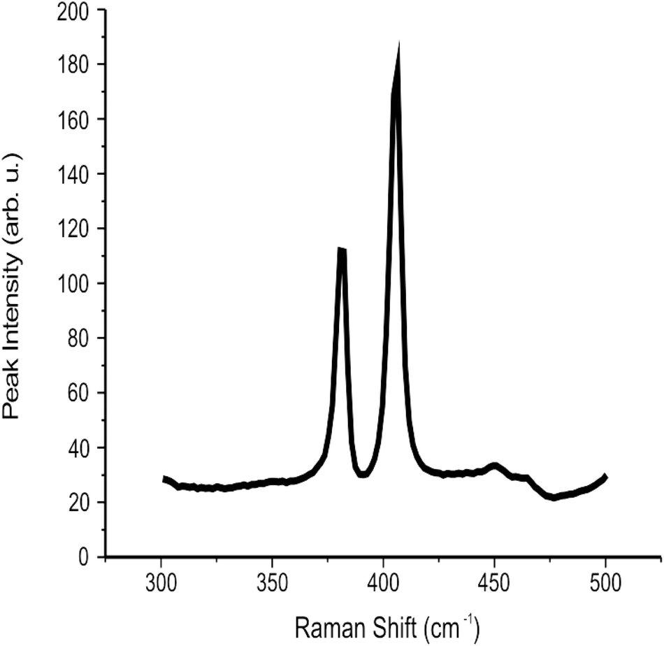 | ||
| Fig. 1 Raman spectra of the commercially sourced 2D MoS2 nanosheets immobilised upon a silicon wafer. | ||
:2.2 ratio respectively, agreeing well with the Raman and EDS analysis performed above (further indicating the presence of the target material). Shin et al.68 theorises the deviation from an expected stoichiometry ratio of 1:2 for Mo and S respectively in 2D MoS2 nanosheets is due to the presence of MoS3.63 It is of note that Mo is present in three valence states, with each of the valence states consisting of a Mo 3d5/2 and Mo 3d3/2 doublet. The curve-fitted high resolution Mo 3d spectral region is shown in ESI Fig. 6.† The area ratios of the doublets are constrained to the ratios of the Scofield cross sections (i.e. Mo 3d3/2 = 0.6904 × Mo 3d5/2), the two components of each doublet are constrained to the same line shape and ‘full width at half maximum’, and their separations are fixed at the known reference value of 3.13 eV. The 3d5/2 components were found at 229.4 eV (Mo4+), 231.6 eV (Mo5+) and 233.1 eV (Mo6+). The spectral region also includes the S 2s peak at 226.6 eV.
3.2 Electrochemical activity at assigned coverage
The electrochemical response of the 2D MoS2 nanosheets (1266.7 ng cm−2) immobilised upon SPEs were studied using cyclic voltammetry (CV). Fig. 2 shows a typically observed CV where two oxidation peaks at +0.65 and +1.0 V are clearly visible in the first cycle followed by several minor reduction peaks in the −0.5 to −1.5 V range. The initiation of the HER is evident in the cathodic response, with an onset potential of ca. −1.1 V. In terms of the anodic response, the two prominent oxidation peaks are due to irreversible reactions, likely the oxidation of Mo4+ to Mo6+ at edge- and basal-plane sites. Such oxidations are not observable in subsequent scans, which is likely due to the MoO3 dissolving into solution or being reduced to Mo3+, at which point it dissolves, explaining the origin of the observed reduction peak. This is represented in the equation below.69| MoS2 + 7H2O → MoO3 + SO42− + ½S22− + 14H+ + 11e− | (3) |
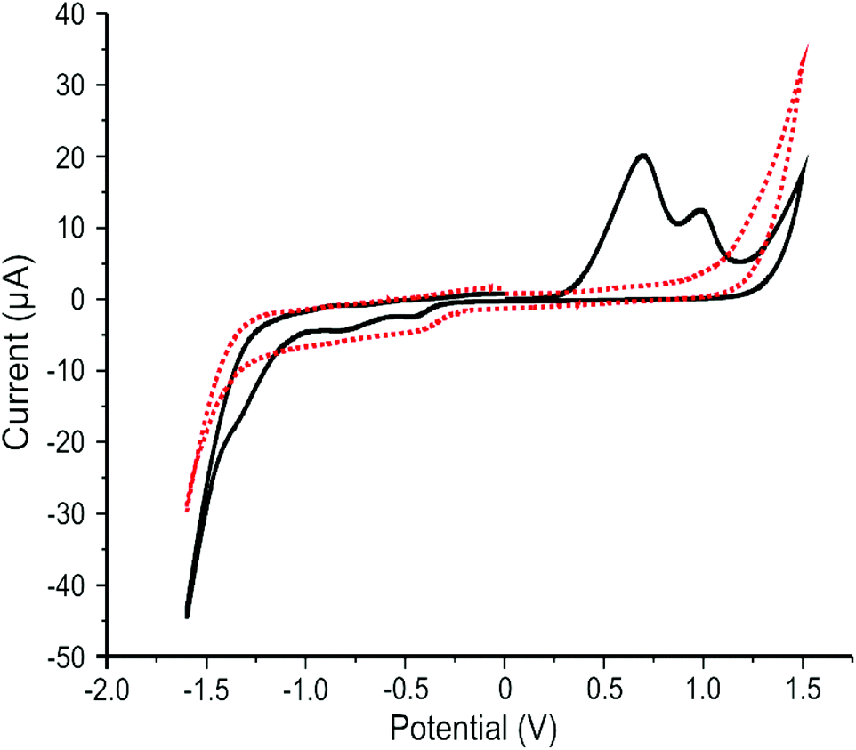 | ||
| Fig. 2 Typical cyclic voltammetric response of 2D MoS2 nanosheets (1266.7 ng cm−2) immobilised upon a SPE in pH 7 phosphate buffer solution (PBS). First scan: solid black line. Second scan (representative of subsequent scans): red dotted line. Scan rate: 5 mV s−1 (vs. SCE). | ||
It may also be possible that the Mo within our 2D MoS2 nanosheets has two dominant valence states, both of which are oxidised, resulting in the presence the double peak. This inference is supported by the independent XPS analysis (see earlier), which indicated the presence of Mo in three different valance states for the 2D MoS2 nanosheet sample analysed. The double oxidation peak observed in Fig. 2 is of interest and further study is required to determine its exact cause. The observed voltammetry (see Fig. 2) is in good agreement with Bonde et al.69 who explored nano-MoS2 deposited onto toray carbon paper in 0.5 M H2SO4 towards the HER. If the potential window is kept below the range where the reported oxidation peaks occur, the HER activity of nano-MoS2 remains stable.70 The reduction peaks can also be accounted for by the reduction of S22− to H2S.69 The double oxidation peak has previously been mischaracterised as a single oxidation peak due to the peaks merging: occurring as a result of performing cyclic voltammetry at too high a scan rate.71 This is important to note as the double peak convolutes the understanding of the electrochemical process occurring.
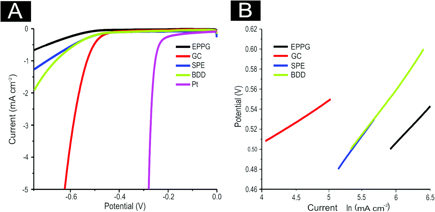
Next, attention was turned to benchmarking our electrochemical system for the HER using commonly available electrodes in 0.5 M H2SO4, as is widespread practise within the literature.14,69,72 As is evident in Fig. 3(A), the four unmodified carbon based electrodes are all significantly inferior to a Pt electrode with respect to the potential required for HER onset and the current density reached. Note that the onset of HER is analysed as the potential at which the observed current initially begins to deviate from background current. Pt′s superior performance is to be expected given it is a pure metal which has a very small binding energy for H+.7 It is evident that the onset potential for the HER occurs at ca. −1.05, −0.78, −0.76 −0.73, and −0.25 V at the GC, EPPG, BDD, SPE, and Pt electrodes respectively. The SPEs exhibit the lowest onset potential for the HER when compared to all of the carbon-based electrodes utilised herein. The bare GC electrode exhibited the largest HER onset potential, indicating that it is not a beneficial electrode for the HER.
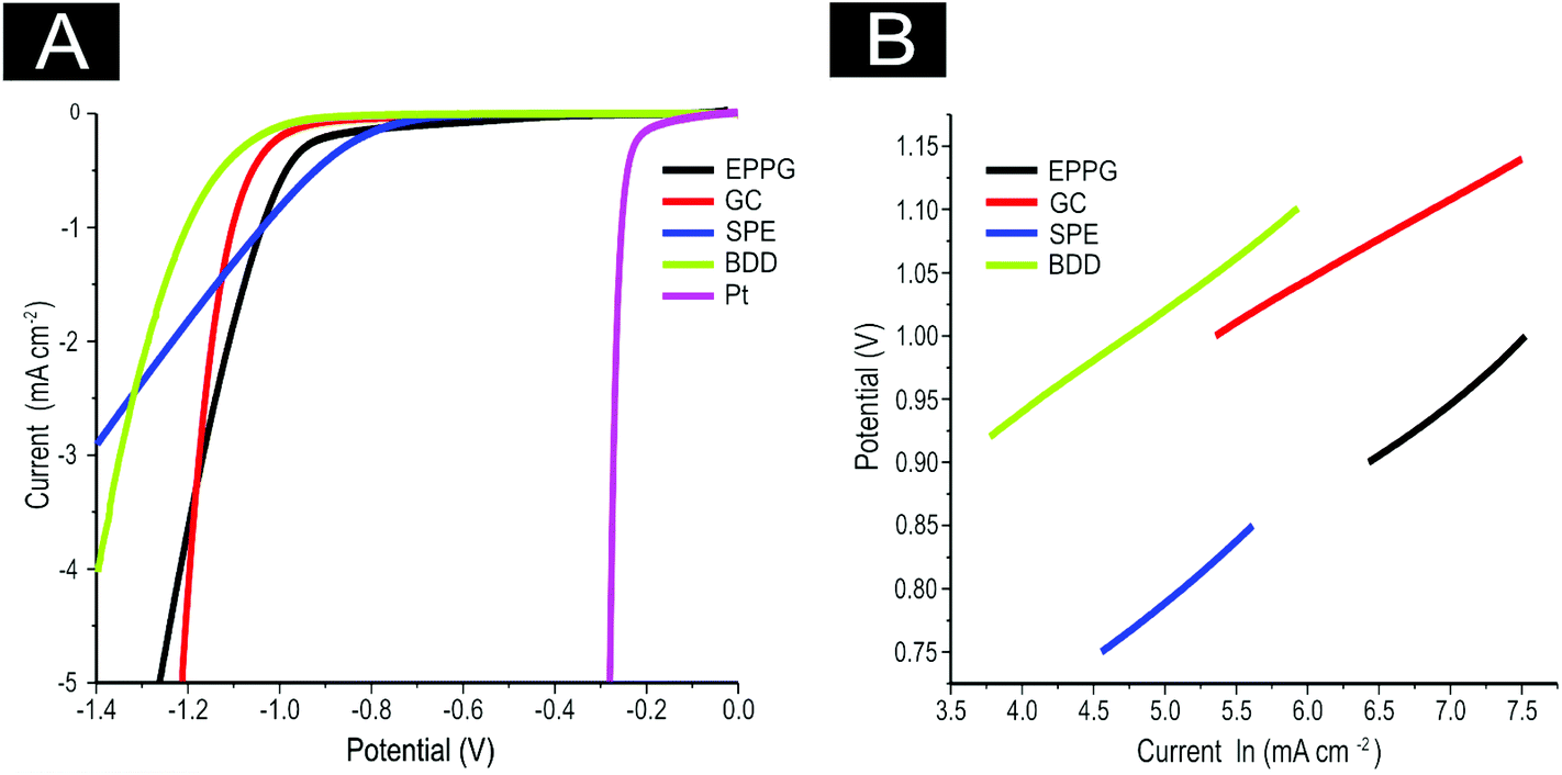 | ||
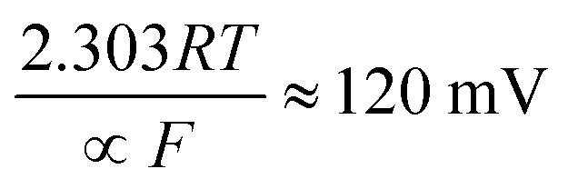
| Fig. 3 (A) Linear sweep voltammetry (LSV) of unmodified EPPG, GC, SPE, BDD and Pt electrodes showing the onset of the HER. In all cases, scan rate: 25 mV s−1 (vs. SCE). Solution composition: 0.5 M H2SO4. (B) Tafel analysis; potential vs. natural log (ln) of current density for faradaic section of the LSV presented in (A). | ||
It is interesting to consider the current density obtained at each of the unmodified electrodes towards the HER and how this progressively alters during the course of the measurement. Although it is apparent that a higher potential is required to initiate the HER at the GC electrode (by ca. −0.3 V in contrast to the alternative carbon based electrodes, making it unfavourable in this sense), the current density recorded at this electrode appears to surpass that of the alternative materials.
| H3O+ (aq) + e− + catalyst → H (ads) + H2O (l) | (4) |
The Volmer step can then be followed by one of two possible steps; either the Heyrovsky step:
| H (ads) + H3O+ (aq) + e− → H2 (g) + H2O (l) | (5) |
or the Tafel step:
| H (ads) + H (ads) → H2 (g) | (6) |
where the transfer coefficient (α) is 0.5, F is the Faraday constant, R is the universal gas constant and T is the temperature at which the electrochemical experiment was performed. Values from the Tafel analysis (presented below each equation) are an indication of the reaction mechanism. Tafel analysis was performed on the Faradaic sections of the LSV plots which can be observed in Fig. 3(A). Tafel analysis was performed on the data presented in Fig. 3(A) where the corresponding analysis is presented in Fig. 3(B), which yielded Tafel values of ca. 89.2, 64.4, 94.4 and 81.2 mV dec−1 for the unmodified EPPG, GC, SPE and BDD electrodes respectively. Using the above values for the unmodified electrodes, interpretation of the Tafel slopes reveals that the adsorption Volmer step is likely rate limiting for the SPE and EPPG electrodes. The discharge Heyrovsky step is most likely the rate limiting step at the GC electrode.11–13 In the case of BDD, Tafel analysis does not allow a definitive mechanism to be estimated.
We next explore the use of 2D MoS2 nanosheet modified carbon based electrodes towards the HER. As detailed in the introduction, the aim of this paper is to tackle the current issue of finding a cheap, more abundant, electrocatalyst alternative to Pt for the HER.7,11 We investigate the potential current state of the art (2D MoS2 nanosheets) and compare this to our benchmarking experiments with the aim of revealing valuable insights. First, the range of carbon based electrodes utilised above (namely GC, BDD, EPPG and SPEs) are modified with different masses of the 2D MoS2 nanosheets. Note that using various underlying support materials is seldom seen in the current literature and thus it is important that such control experiments are explored and reported herein for the first time. Inspection of Fig. 4(A) reveals that using a 1267 ng cm−2 modification of 2D MoS2 nanosheets results in a lowering of the potential required for onset of the HER and is accompanied by an increase in the observed current density, signifying an improved electrochemical response at each of the underlying electrode substrates utilised. Specifically, the HER onset potential was lowered to ca. −0.45, −0.48, −0.44 and −0.45 V for EPPG, GC, SPE, and BDD electrodes respectively. Clearly, these newly obtained values are significantly closer to the reported value using a Pt electrode (ca. −0.25 V) than the initial values reported above at the unmodified carbon based electrodes. This implies that the 2D MoS2 nanosheet is an effective electrocatalyst for the HER.
 | ||
| Fig. 4 (A) LSV of 1267 ng cm−2 2D MoS2 nanosheet modified EPPG, GC, SPE, BDD electrodes and an unmodified Pt electrode showing the onset of the HER. In all cases, scan rate: 25 mV s−1 (vs. SCE). Solution composition: 0.5 M H2SO4. (B) Tafel analysis; potential vs. natural log (ln) of current density for Faradaic section of the LSV presented in (A). | ||
Tafel analysis was performed on the modified LSV profiles. Tafel slope values of ca. 74.7, 41.4, 90.0, and 90.9 mV dec−1 were estimated at the EPPG, GC, SPE and BDD electrodes respectively (shown in Fig. 4(B)). Comparison of the Tafel values suggests that modification of the support electrodes with 2D MoS2 nanosheets does not cause a significant alteration in the mechanism or indeed the Faradic current density of the HER.42 This however, is not the case when utilising the GC electrode, which exhibited a reasonable increase in current density resulting in the ‘discharge Heyrovsky’ step more likely becoming the rate limiting step. This implies that modification with the 2D MoS2 nanosheets allows for increased and sufficient H+ adsorption, thus in turn catalysing the HER process.
In terms of analysing the current densities obtained, deposition of the 2D MoS2 nanosheets at a coverage of 1266.7 ng cm−2 induces higher exchange current densities when compared to the unmodified alternative. It is likely that this results from the early onset of the HER (i.e. the decreased over-potential) and is not directly due to an overall increased reaction rate at the modified SPE and BDD electrodes given that comparison is based on analysis at specific potentials. For the GC and EPPG electrodes there was an increase in the current density, which is due not only the earlier HER onset potential but also an increased current density slope. This is likely a result of the structure of MoS2 on these electrodes having a high number of exposed active edge sites allowing for a greater amount of H+ adsorption.
3.3 Electrochemical activity at differing 2D MoS2 nanosheet coverages
In order to ascertain the level of MoS2 coverage and relate this to the observed voltammetry, we first investigate the respective Raman properties of our modified electrodes. Fig. 5 depicts the effect that larger deposition quantities of MoS2 onto a SPE has upon the recorded Raman Spectroscopy, where the evolution of the two characteristic peaks is evident and is discussed in more detail below. We first analyse the effect of coverage on the electrode surface using Raman mapping and a SPE as the underlying support material (as a representative model). Through comparison of the underlying graphite peak area at ca. 1550 cm−1 against the area of the MoS2 Raman peaks at ca. 380 and 405 cm−1, the surface area coverage of the electrode was investigated. It is evident that increasing the mass deposition of MoS2 on the SPE surface results in an increased intensity in the respective assigned Raman peaks (see Fig. 5(A)). Raman maps are presented in Fig. 6 which concur with the previous inference and show that with increased mass deposition a thicker (largely uniform) layered coverage is achieved across the entire electrode surface. Through analysis of the respective Raman maps depicted in Fig. 6 and 7, it is likely that the deposition of 504 ng cm−2 2D MoS2 nanosheets results in the complete coverage of the underlying SPE support material (which has a surface area of 0.0707 cm2). With each additional modification this layer of deposited MoS2 will thicken (see Fig. 7). It is possible to determine the stacking number by comparison of E12g and A1g vibrational bands (VB) as the observed Raman spectrum evolves with the number of layers present. The E12g VB results (at ca. 382 cm−2) due to the opposite vibration of two S atoms in respect to a Mo atom, whereas the A1g peak (at ca. 407 cm−2) represents the S atoms vibrating in opposite directions and out of plane.67,73 Literature suggests that as MoS2 moves from single layer to bulk the E12g VB downshifts from 384 to 382 cm−2, whilst A1g VB shifts upwards from 403 to 408 cm−1, where a separation of ca. 19 cm−1 between the VBs is indicative of single layer MoS2 and a value of ca. 25 cm−1 represents the bulk material.26,40,73 In this work we observe an increase in the Raman shift of the E12g VB with greater mass additions from ca. 377 to 380 cm−1,(see Fig. 5(A)), however the response observed herein may result from the specific morphology and stacking structures of our MoS2 on the underlying support material given that previous studies have reported a similar shift relating to the E12g band and attributed this to uniaxial strain or heterostructure stacking.74 Interestingly, analysis of the A1g peak corresponds to the predicted theorem for a transition from single-layer to multi-layer 2D MoS2 nanosheets with an increasing Raman shift from ca. 402 to 405 cm−1.40,67
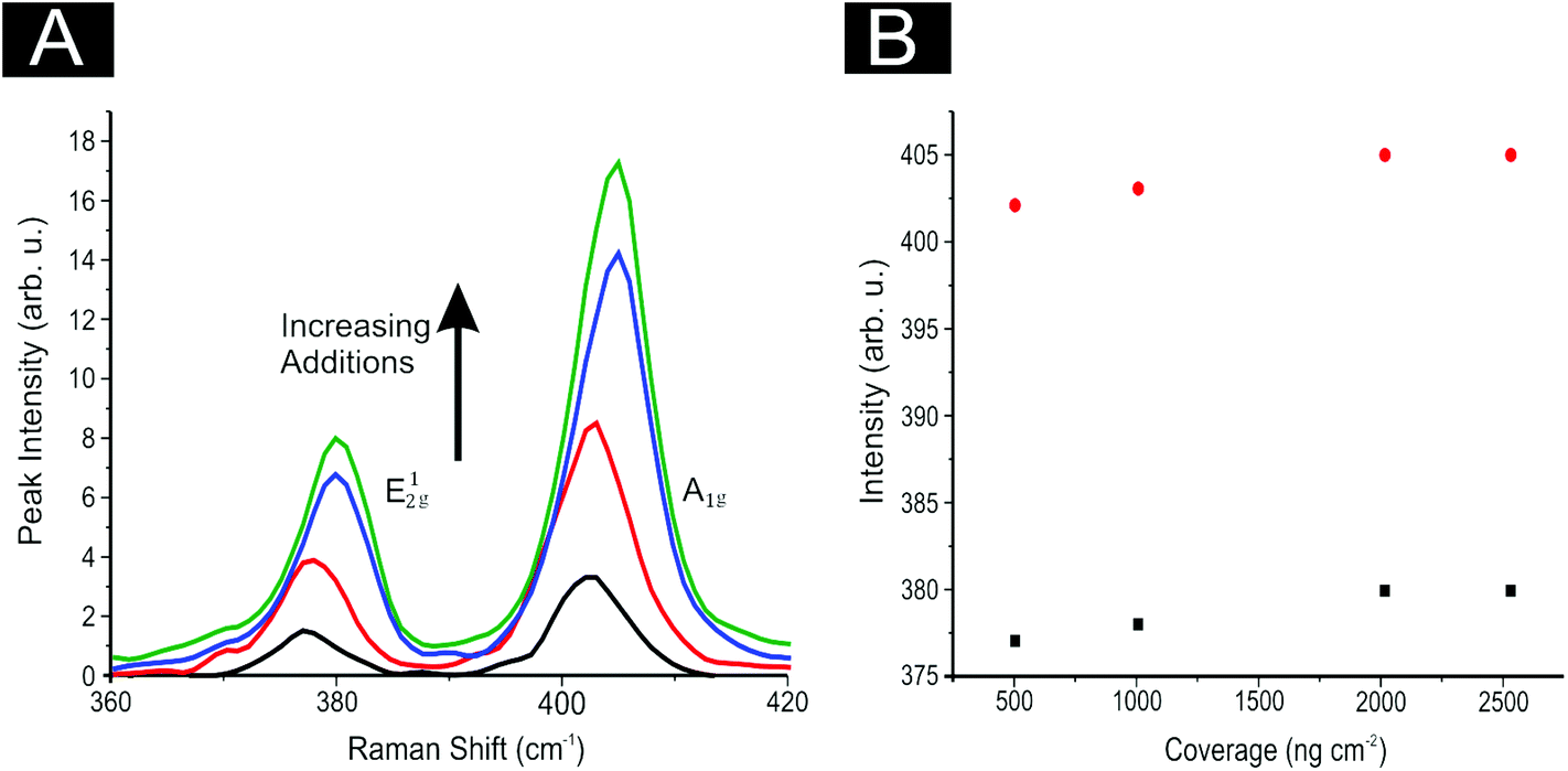 | ||
| Fig. 5 (A) Raman spectra peak intensity and position for 504 (black), 1009 (red), 2019 (blue) and 2533 (green) ng cm−2 2D MoS2 nanosheet modifications on SPEs. (B) Depicts 2D MoS2 nanosheet coverage plotted against Raman peak intensity for E12g (black) and A1g (red) vibrational bands, showing a constant peak distance of 24.7 cm−1 at all coverages. | ||
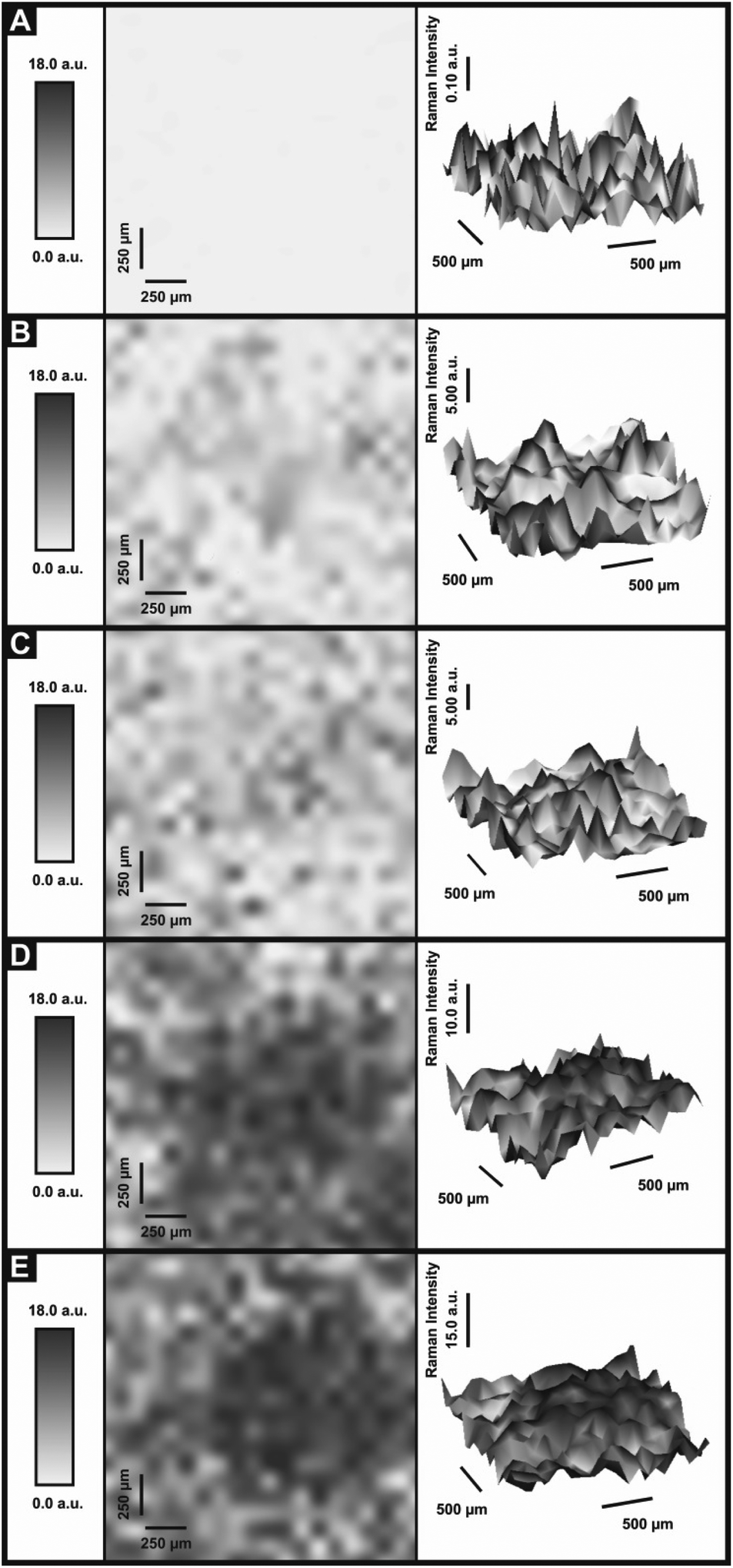 | ||
| Fig. 6 Raman maps representing various MoS2 coverages onto an underlying SPE. Coverages of 2D MoS2 nanosheets: 0 (A), 504 (B), 1009 (C), 2019 (D), and 2533 (E) ng cm−2. Raman intensities recorded at 405 cm−1. | ||
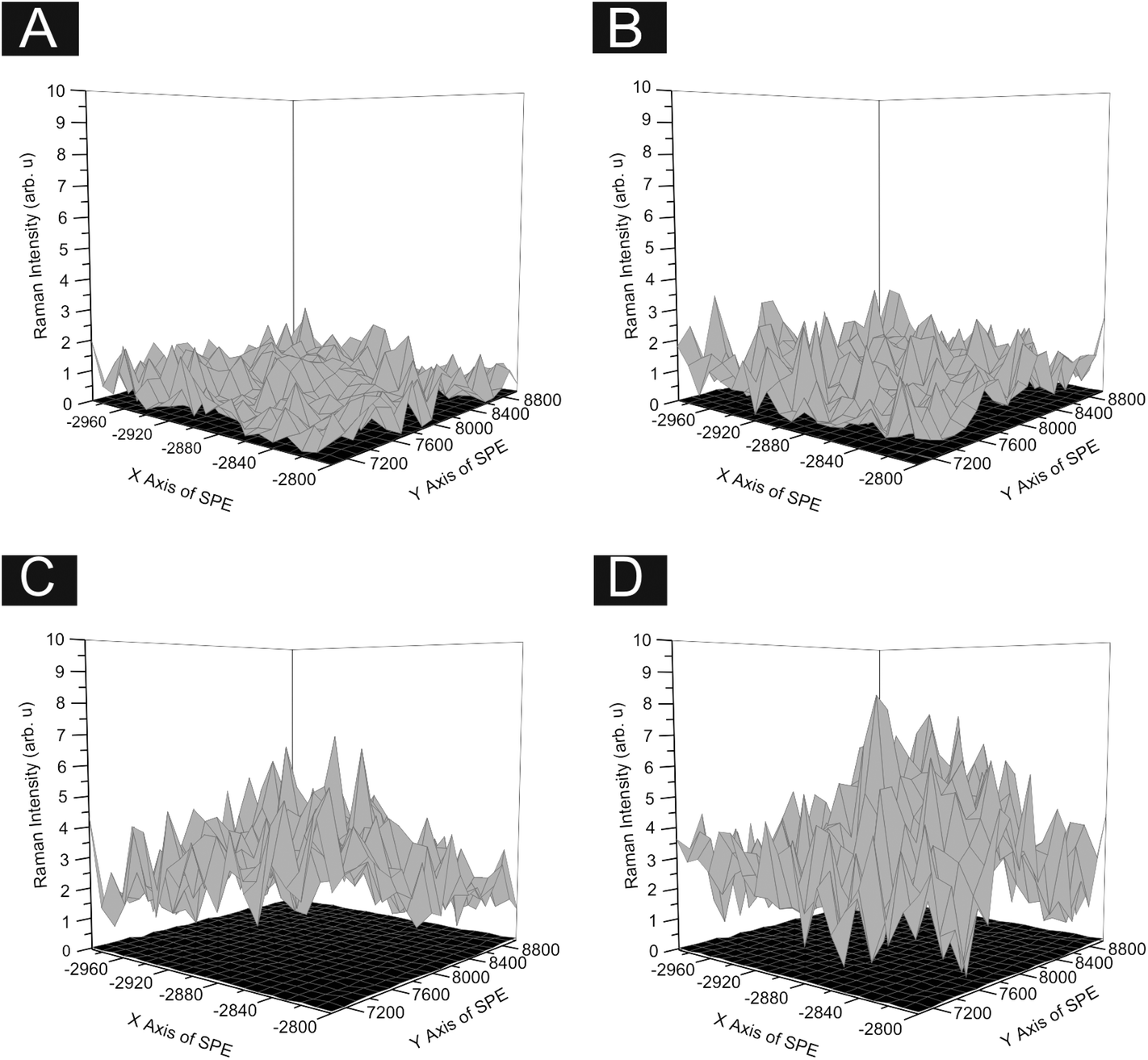 | ||
| Fig. 7 Raman maps of SPE surface, each point showing the intensity ratio between the sum of the characteristic MoS2 peak areas (380 and 405 cm−1) against the area of the underlying graphite peak (1550 cm−1). Using varying surface coverages of our 2D MoS2 nanosheets; 504 (A), 1009 (B), 2019 (C) and 2533 (D) ng cm−2. The grey maps are the modified electrodes and the black map in each represents an unmodified electrode surface. | ||
Furthermore, when considering the separation of the two VBs (given that this value is also indicative of the number of MoS2 layers present) the shift in the difference of the VB positions between A1g and E12g gives a consistent value of 24.7 cm−1 with increasing coverages, indicating that +4 layers (i.e. bulk) MoS2 is present at all four mass coverages utilised herein (see Fig. 5(B)). Consideration of the above factors in conjunction with our independent lateral grain size calculations (UV-VIS) indicates that the structural model of the 2D MoS2 nanosheets utilised herein is likely that of re-assembly, with the few-layer nanosheets forming bulk MoS2 upon deposition onto the electrode surface. Further work on whether the morphology of a SPEs surface causes uniaxial strain and/or heterostructure stacking of the 2D MoS2 nanosheets would be of great interest. Note that confirmatory tests were performed in which the aliquots deposited above were immobilised onto an alternative silicon wafer support in order to overcome potential issues with the underlying surface. Such control experiments (data not shown) exhibited the same separation values as identified above (ca. 25.1 cm−1) between the two VBs and thus confirms that our 2D MoS2 nanosheets likely form bulk MoS2 once deposited/immobilised onto a support surface. It is likely that further additions of our material result in the formation of thicker or rougher ‘bulk’ layers. We next explore the electrochemical implications of this, often overlooked in the literature.
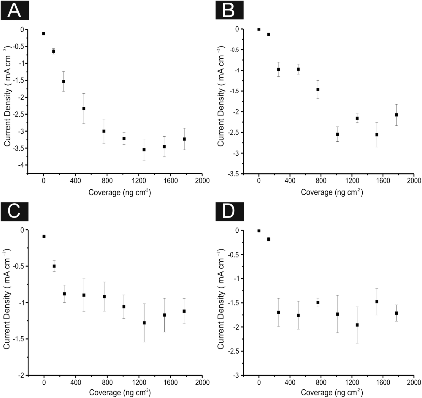 | ||
| Fig. 8 Current density values taken at −0.75 V from linear sweep voltammetry from 0, 128.6, 252, 504, 762. 1009, 1267, 1524 and 1771 ng cm−2 2D MoS2 nanosheets immobilised upon: (A) EPPG, (B) GC, (C) SPE (D) BDD. Each graph showing the plateauing effect of current density when a critical mass of the 2D MoS2 nanosheets is deposited onto the electrodes surface. Error bars are the average and standard deviation of 3 replicates. | ||
3.4 Assessment of 2D MoS2 nanosheets catalytic activity
An array of approaches are employed to study the intrinsic catalytic activity of 2D MoS2 nanosheets within the literature. In order to deduce how the observable catalytic activity alters with changes in the mass of 2D MoS2 nanosheet modification we employ two commonly used techniques below: the assessment of catalytic turn over frequency (ToF) and the number of active sites present on the surface of the electrode.47,68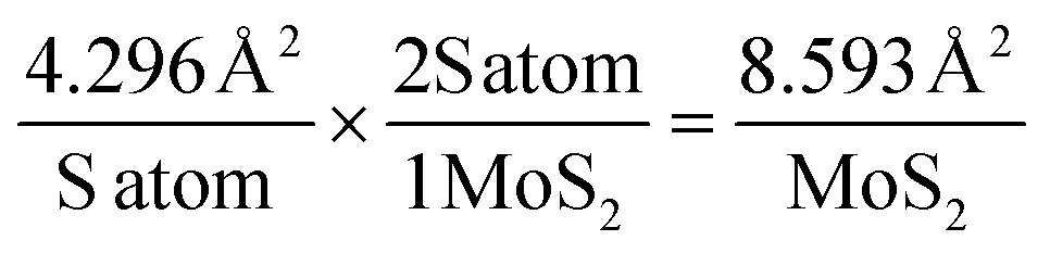 | (7) |
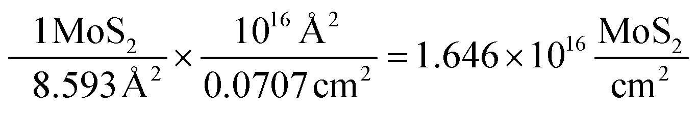
Using the derived area for a MoS2 molecule (corresponding to the number of surface sites for a flat standard) it is possible to determine the number of MoS2 molecules per cm2 geometric area:
 | (8) |
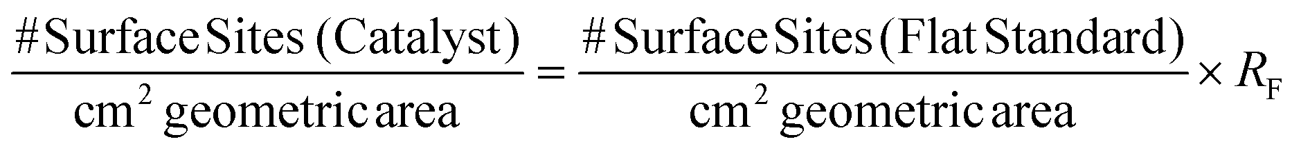
The number of electrochemically accessible surface sites can be determined from the following:
 | (9) |
It is also essential to accurately determine the roughness factor (RF) for each modified electrode surface which was performed using white light profilometry (WLP) (See ESI Fig. 7†) as is common within the literature. The described WLP technique yielded RF values which represent the entire surface area of the electrode rather than electroactive area (see later). In the case of the 252 ng cm−2 modified SPE, the number of surface sites cm−2 corresponds to 3.16 × 10¹⁶ surface sites per cm2. The following allows the ToF on a per-site basis to be determined:
 | (10) |
Taking the value of current density (mA cm−2) at the potential of −0.75 V (at a 100 mV s−1 scan rate) and using the RF calculated via WLP, per-site the ToF can be deduced from the following:
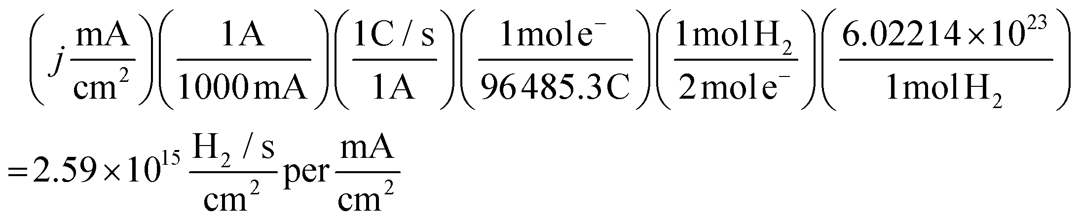 | (11) |
Using eqn (12) and a value derived from formula (11), it is possible to determine a value for the ToF:
 | (12) |
At the chosen potential (−0.75 V) the current densities were found to correspond to 0.83, 1.16 and 1.17 mA cm−2 for SPEs (SPEs used as representative example of the carbon based electrodes utilised) modified with 252, 1009 and 2019 ng cm−2 of 2D MoS2 nanosheets. The RF values calculated via the WLP method (which provides the topography of the uppermost surface, see roughness factor calculation method 1 in the ESI†) were found to correspond to 1.918, 1.934 and 1.924 respectively. Using these values the ToF values deduced from the above equations were found to correspond to 0.81, 1.14 and 1.15  . The stability of the WLP RF values across the range of modifications results in relatively little variation of the ToF values obtained. Benck et al.47 suggest that the upper and lower possible ToF could be one order of magnitude greater or less than the given value. If the chosen potential is altered to −1.5 V the current densities at this potential correspond to 4.25, 4.43 and 4.33 mA cm−2 for the 252, 1009 and 2019 ng cm−2 2D MoS2 nanosheet modified SPEs respectively. Using the same technique and WLP RF values above, however replacing the current densities at −0.75 V for those at −1.5 V the ToF values are 0.59, 0.61 and 0.6
  for the 252, 1009 and 2019 ng cm−2 2D MoS2 nanosheets modified SPEs respectively. Clearly, altering the potential at which the current densities are recorded has a significant affect upon the ToF recorded.
In order to deduce RF values which are representative of the true electroactive area of an electrode, a double layer capacitance technique can be employed (see roughness factor calculation method 2 in the ESI†). The double layer capacitance technique is preferential to the WLP technique as it describes the true electroactive surface area of the electrode, including accessible pores and the thickness of multiple layers deposited, whereas WLP is limited in that it bases its calculated value off only a scan of the topography of the uppermost surface in question; simply, the WLP only probes the outermost layer and cannot determine a relatively thick layer from a thin layer. The double layer capacitance technique for determining RF is reported in the ESI.†
Taking the current density values corresponding to a −0.75 V potential and replacing the WLP RF values for 1.0, 3.3 and 4.8 which are the RF values calculated via double layer capacitance, for SPEs modified with 252, 1009 and 2019 ng cm−2 of 2D MoS2 nanosheets, the ToF was found to correspond to 1.58, 0.6 and 0.46  . The values estimated for the ToF herein are in rough agreement with the range of ToF values Xie et al.77 states should be expected for various types of MoS2 structures. It is evident that, as a result of increasing the mass of 2D MoS2 nanosheets deposited onto an SPE, there is a resulting decrease in the ToF
  . This is possibly the result of larger masses of 2D MoS2 nanosheets, once deposited, forming a MoS2 structure whereby there is increased shielding of active edge sites by inactive basal planes.42,47 Again, if the current densities are altered to those corresponding to a −1.5 V potential whilst using the same technique and double layer capacitance RF values, above, the ToF values deduced are 1.14, 0.37 and 0.24
  for the 252, 1009 and 2019 ng cm−2 2D MoS2 nanosheets modified SPEs respectively. Of note is the significant affect that altering the potential at which the current densities are measured has upon the determined ToF values. This ability to manipulate the ToF value deduced makes it essential for literature to create an industry standard for what potentials should be used when dealing with ToF calculations. This would allow for more ready comparison between different studies involving ToF.
As previously stated the double layer capacitance technique provides a true electrocatalyic surface area of the given electrode whereas the WLP technique provides a scan of topography of the uppermost surface. It can therefore be assumed that the RF values deduced via double layer capacitance offer more accurate ToF values.
| N = RF(NAd/Mf)2/3 | (13) |
| Electrode | MoS2 modification (ng cm−2) | Roughness factor | Number of active sites |
|---|---|---|---|
| BDD | 2019 | 2.2 | 2.01 × 10¹² |
| 1009 | 1.5 | 1.38 × 10¹¹ | |
| 252 | 0.3 | 3.03 × 10¹¹ | |
| EPPG | 2019 | 7.7 | 7.05 × 10¹² |
| 1009 | 5.5 | 5.05 × 10¹² | |
| 252 | 4.2 | 3.84 × 10¹² | |
| GC | 2019 | 2.6 | 2.35 × 10¹² |
| 1009 | 2.1 | 1.95 × 10¹² | |
| 252 | 1.0 | 8.95 × 10¹¹ | |
| SPE | 2019 | 4.8 | 4.43 × 10¹² |
| 1009 | 3.3 | 3.00 × 10¹² | |
| 252 | 1.0 | 9.36 × 10¹¹ | |
It is evident that the increased mass deposition of 2D MoS2 nanosheets on a given electrode surface results in an improvement in the current passed in addition to a lowered HER onset potential (improved electrochemical response). As is apparent from the above discussion (and inspection of Fig. 8) this increase in the catalytic performance at a given modified electrode material (which corresponds to the addition of 2D MoS2 nanosheets) reaches a plateau after which further additions of our target material do not result in an improved electrochemical performance. This ‘critical mass’ of modification is likely due to the structure of the 2D MoS2 nanosheet altering to that of a bulk formation (see earlier), thereby exposing less edge sites and thus inhibiting the beneficial electrochemical properties of single-, few-, quasi- MoS2 nanosheets. Alternatively, this plateau could signify the mass (a critical mass of ca. 1009 ng cm−2 of the 2D MoS2 nanosheets) at which the structure of MoS2 can no longer structurally support itself upon the electrode surface (becoming unstable), diminishing and detaching from the surface of the electrode, eliminating the catalytic advantages of further additions (such that in some cases the catalytic response begins to deteriorate). Similar observations have been reported for the case of graphene.79–82 This could arise due to the disconnection of 2D MoS2 nanosheet layers during the course of the experiment (i.e. instability of the modified layer on the electrode surface due to the large quantity/mass present) which is bought about once such a ‘critical mass’ is achieved.
The intra-repeatability of the modified and unmodified SPEs were tested (N = 3). The % Relative Standard Deviation (% RSD) in the onset potential of the HER was found to be ca. 0.8, 1.4, 1.5, and 4.6% at the 0 (unmodified), 252, 1009 and 2019 ng cm−2 2D MoS2 nanosheet modified SPEs respectively. It is clear that the % RSD increases with greater modifications of the MoS2, likely a result of the factors stated above and potentially resulting in the reduced catalytic effects. Furthermore, the % RSD in the current densities observed were found to be ca. 12.4, 13.5, 10.5, and 15.5% at the 0 (unmodified), 252, 1009 and 1771 ng cm−2 2D MoS2 nanosheet modified SPEs respectively. The high RSD values in this case are indicative of the structural instability of the deposited 2D MoS2 nanosheet film on the underlying electrode surface, which likely leads to delamination and thus high levels of variation within the effective surface area and currents passed.
From the above inferences, we suggest that the structural model of 2D MoS2 nanosheets is likely that of re-assembly, such that upon modification with increasing amounts of 2D MoS2 nanosheets, bulk layers of MoS2 materialise upon the surface of our support electrodes.79,81
Electrochemical impedance spectroscopy (EIS) was used to determine the impedance of the electrode system as the coverage of 2D MoS2 nanosheets was increased, see ESI Fig. 10.†70 It was observed that the charge transfer resistance (Ω) for all electrodes decreased after modification with 252 ng cm−2 2D MoS2 nanosheets and further decreased after modification with 1009.5 ng cm−2. Again a plateauing was observed in the response with increased coverage (for example after modification with 2019 ng cm−2). The Ω values of the unmodified SPE (3.51 × 10⁵ Ω) reduced to 1.69 × 10⁵ Ω after 252 ng cm−2 and then to 3.27 × 10³ Ω upon a 1009 ng cm−2 2D MoS2 nanosheet modification, after which the response plateaued, having an impedance value of 3.21 × 10³ Ω by modification with 2019 ng cm−2. Error values for the aforementioned results were recorded as 1.78 × 10⁻⁴, 1.73 × 10⁻³, 1.2 × 10⁻², and 1.21 × 10⁻² Ω respectively. This EIS supports the above inferences and indicates that the 2D MoS2 is an effective electrocatalyst with respect to the HER when deposited on a carbon electrode surface.
Finally, it is essential to assess the electrochemical stability of 2D MoS2 nanosheets as a catalyst for the HER when drop coated onto an electrode surface (following on from the reported % RSD values noted above). This is a practical consideration for real applications where durability and longevity are necessary.2,27,68 SPEs were used as a representative example for the four carbon based electrodes used within this study. A 1000 cycle voltammetry scan from 0 to −0.8 V at 25 mV s−1 was performed on SPEs modified with 252, 1009, 2019 ng cm−2 of 2D MoS2 nanosheets. A decrease in the catalytic activity of each electrode was observed (see Fig. 9). At 0.6 V the decrease from the initial scan current was 6.8%, 32.3%, 26.9% for the SPEs modified with 252, 1009 and 2019 ng cm−2 respectively. The observed activity loss is significant, especially for the 1009 and 2019 ng cm−2 modified electrodes. According to Shin et al.68 high stability of amorphous MoS2 is rarely reported with the decrease in activity being associated with either: surface absorbatives which may poison the active sites of the 2D MoS2 nanosheets;47 or the delamination of the 2D MoS2 nanosheets from the substrate.47 However, it is likely a combination of these two effects with the delamination of 2D MoS2 nanosheets becoming more prevalent at higher modifications. This inference is supported by the EIS observations detailed earlier.
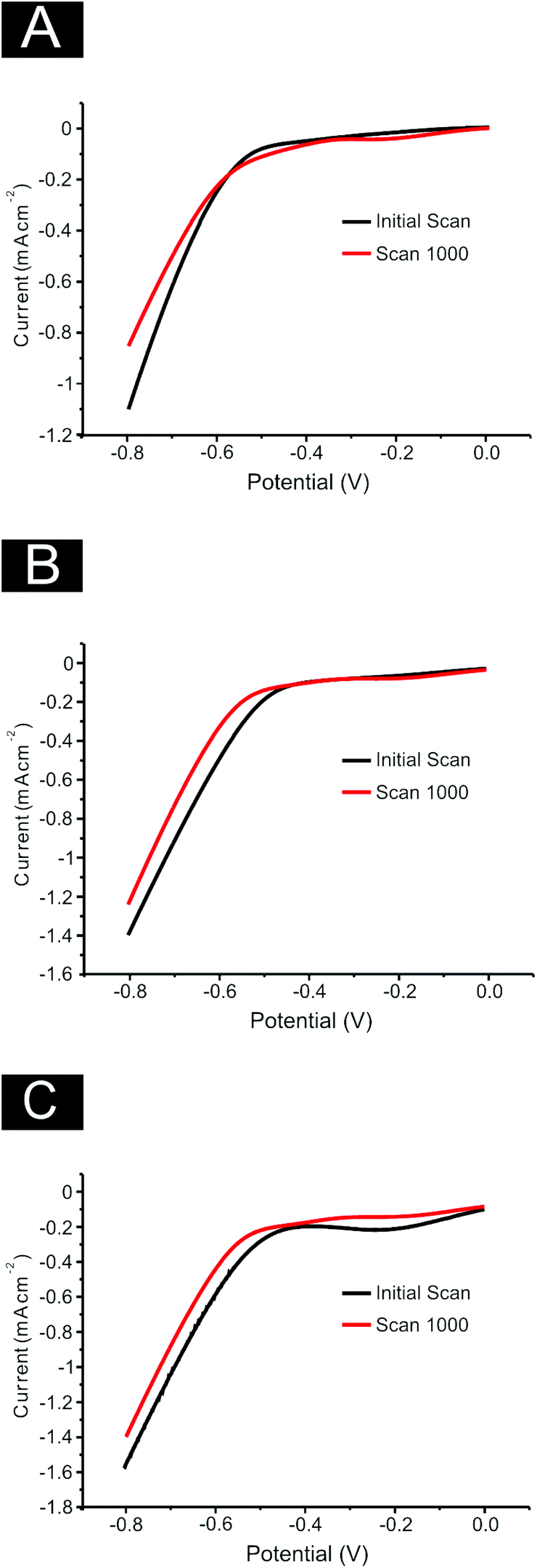 | ||
| Fig. 9 Stability studies using SPEs modified with (A) 252, (B) 1009 and (C) 2019 ng cm−2 2D MoS2 nanosheets. Cyclic Voltammetry was performed between the potential range of 0 to −0.8 V, repeated for 1000 cycles, these figures show the initial (black line) and 1000th (red line) scans. Scan rate: 25 mVs−1 (vs. SCE). | ||
Another consideration in terms of industrial application is cost of the four carbon based electrodes studied, the GC offered the greatest current density and most noted HER onset potential decrease upon modification with 2D MoS2 nanosheets. GC's production cost makes its application as a catalyst on an industrial scale economically unfeasible. The SPE offers an attractive alternative to using GC in real-world industrial applications. After modification with 2D MoS2 nanosheets, the HER onset potential is lowered to a value equivalent of GC's. One issue could potentially be that the modified SPE exhibits a lower current density compared to that of GC, however, due to the nature of SPE's production they have can be produced to a wide manner of tailorability, varying in shape, surface area and carbon composition. As such SPEs can be produced with a larger surface area than that of GC, thereby increasing the currents possible and ultimately the amount of hydrogen produced. This combined with the ultra-low cost of fabricating SPEs makes them an exceptionally cost effective and easily producible supporting electrode material for HER. There is potential to incorporate 2D MoS2 nanosheets into the carbon based inks used to produce SPEs, thereby eliminating the time consuming modification step. However, further research aimed at identifying and resolving the reason for the poor catalytic stability is essential if 2D MoS2 nanosheet modified SPEs have a future industrial application.
4. Conclusions
We have explored the catalytic performance of 2D MoS2 nanosheets towards the HER. In order to overcome issues prevalent within the literature and to enable us to ascertain the true electrochemical performance of our commercially sourced MoS2 we modified a range of carbon based underlying support electrodes, namely GC, BDD, EPPG and SPEs; this approach is usually neglected within the literature. Application of the MoS2 modified electrodes revealed a catalytic performance towards the HER, with lower onset potentials and higher current densities observed when utilising our target material. The supporting electrode was found to be of key importance, influencing the improvements observed in the electrochemical performance. This work indicates that 2D MoS2 nanosheet modified electrodes can potentially serve as a viable, low cost and more abundant replacement to current Pt based electro-catalysts.This work is distinct from the literature given that we have also correlated our electrochemical responses with supplementary Raman mapping of the electrode surface (and other complementary physicochemical characterisation) whilst exploring the effect of MoS2 coverage. Coverage studies revealed that the catalytic effect of the 2D MoS2 nanosheets increased (as indicated by ToF and ‘number of active sites’ calculations) until a ‘critical mass’ (coverage) was achieved, after which the response was observed to plateau. The likely cause of this effect is inferred herein and has clear implications (in this case and) when employing other 2D nanosheet modified electrodes within the literature.
We have provided insights into the observable electrochemistry and HER mechanism prevalent at 2D MoS2 nanosheet modified electrodes, which has clear potential to be beneficially applied/utilised as an electrocatalyst if the diligent control measures reported herein are sufficiently applied.
Acknowledgements
D. A. C. Brownson acknowledges funding from the Ramsay Memorial Fellowships Trust and a British Council Institutional Link grant (No. 172726574) for the support of this research.References
- Y. Z. Yufei Zhao, Z. Yang, Y. Yan and K. Sun, Sci. Technol. Adv. Mater., 2013, 14 Search PubMed.
- T. Wang, L. Liu, Z. Zhu, P. Papakonstantinou, J. Hu, H. Liu and M. Li, Energy Environ. Sci., 2013, 6, 625–633 CAS.
- A. J. López-Menéndez, R. Pérez and B. Moreno, J. Environ. Manage., 2014, 145, 368–373 CrossRef PubMed.
- T. D. M. G. Schultz, G. P. Brasseur and W. Zittel, Science, 2003, 302, 624–627 CrossRef PubMed.
- T. Hua, R. Ahluwalia, L. Eudy, G. Singer, B. Jermer, N. Asselin-Miller, S. Wessel, T. Patterson and J. Marcinkoski, J. Power Sources, 2014, 269, 975–993 CrossRef CAS PubMed.
- J. Andrews and B. Shabani, WIREs Energy Environ., 2014, 3, 474–489 CrossRef PubMed.
- B. Hinnemann, P. G. Moses, J. Bonde, K. P. Jørgensen, J. H. Nielsen, S. Horch, I. Chorkendorff and J. K. Nørskov, J. Am. Chem. Soc., 2005, 127, 5308–5309 CrossRef CAS PubMed.
- M. Gratzel, Inorg. Chem., 2005, 44, 6841–6851 CrossRef PubMed.
- J. P. Barton and D. G. Infield, IEEE Trans. Energy Convers, 2004, 19, 441–448 CrossRef.
- F. Blaabjerg, Z. Chen and S. B. Kjaer, IEEE Trans. Power Electron., 2004, 19, 1184–1194 CrossRef.
- N. M. Marković and P. N. Ross Jr., Surf. Sci. Rep., 2002, 45, 117–229 CrossRef.
- N. M. Marković, B. N. Grgur and P. N. Ross, J. Phys. Chem. B, 1997, 101, 5405–5413 CrossRef.
- A. B. Laursen, S. Kegnaes, S. Dahl and I. Chorkendorff, Energy Environ. Sci., 2012, 5, 5577–5591 CAS.
- T. F. Jaramillo, K. P. Jørgensen, J. Bonde, J. H. Nielsen, S. Horch and I. Chorkendorff, Science, 2007, 317, 100–102 CrossRef CAS PubMed.
- B. X. Ya Yan, Z. Xu and X. Wang, ACS Catal., 2014, 693–1705 Search PubMed.
- K. Ravindra, L. Bencs and R. Van Grieken, Sci. Total Environ., 2004, 318, 1–43 CrossRef CAS.
- R. L. McCreery, Chem. Rev., 2008, 108, 2646–2687 CrossRef CAS PubMed.
- D. A. C. Brownson and C. E. Banks, Electrochem. Commun., 2011, 13, 111–113 CrossRef CAS PubMed.
- M. Lu, K. E. Toghill and R. G. Compton, Electroanalysis, 2011, 23, 1089–1094 CrossRef CAS PubMed.
- M. Musameh, J. Wang, A. Merkoci and Y. Lin, Electrochem. Commun., 2002, 4, 743–746 CrossRef CAS.
- A. Koca, Int. J. Hydrogen Energy Int., 2009, 34, 2107–2112 CrossRef CAS PubMed.
- Y. Shen, J. Liu, J. Jiang, B. Liu and S. Dong, J. Phys. Chem. B, 2003, 107, 9744–9748 CrossRef CAS.
- J. Yin, J. B. Jia and L. D. Zhu, In, 2008, 33, 7444–7447 CAS.
- Y. Zheng, Y. Jiao, Y. Zhu, L. H. Li, Y. Han, Y. Chen, A. Du, M. Jaroniec and S. Z. Qiao, Nat. Commun., 2014, 5 Search PubMed.
- Z. Chen, D. Cummins, B. N. Reinecke, E. Clark, M. K. Sunkara and T. F. Jaramillo, Nano Lett., 2011, 11, 4168–4175 CrossRef CAS PubMed.
- D. Y. Chung, S.-K. Park, Y.-H. Chung, S.-H. Yu, D.-H. Lim, N. Jung, H. C. Ham, H.-Y. Park, Y. Piao, S. J. Yoo and Y.-E. Sung, Nanoscale, 2014, 6, 2131–2136 RSC.
- Y. Li, H. Wang, L. Xie, Y. Liang, G. Hong and H. Dai, J. Am. Chem. Soc., 2011, 133, 7296–7299 CrossRef CAS PubMed.
- D. Merki, S. Fierro, H. Vrubel and X. Hu, Chem. Sci., 2011, 2, 1262–1267 RSC.
- Q. Liu, J. Tian, W. Cui, P. Jiang, N. Cheng, A. M. Asiri and X. Sun, Angew. Chem., Int. Ed., 2014, 126, 6828–6832 CrossRef PubMed.
- L. F. Pan, Y. H. Li, S. Yang, P. F. Liu, M. Q. Yu and H. G. Yang, Electrochem. Commun., 2014, 50, 13135–13137 CAS.
- Y. H. Chang, C. T. Lin, T. Y. Chen, C. L. Hsu, Y. H. Lee, W. J. Zhang, K. H. Wei and L. J. Li, Adv. Mater., 2013, 25, 756–760 CrossRef CAS PubMed.
- P. Joensen, E. D. Crozier, N. Alberding and R. F. Frindt, J. Phys. C: Solid State Phys., 1987, 20, 4043–4053 CrossRef CAS.
- J. H. Lee, W. S. Jang, S. W. Han and H. K. Baik, Langmuir, 2014, 30, 9866–9873 CrossRef CAS PubMed.
- S. Ji, Z. Yang, C. Zhang, Z. Liu, W. W. Tjiu, I. Y. Phang, Z. Zhang, J. Pan and T. Liu, Electrochim. Acta, 2013, 109, 269–275 CrossRef CAS PubMed.
- B. Radisavljevic, A. Radenovic, J. Brivio, V. Giacometti and A. Kis, Nat. Nanotechnol., 2011, 6, 147–150 CrossRef CAS PubMed.
- S. Tongay, J. Zhou, C. Ataca, K. Lo, T. S. Matthews, J. Li, J. C. Grossman and J. Wu, Nano Lett., 2012, 12, 5576–5580 CrossRef CAS PubMed.
- M.-L. Tsai, S.-H. Su, J.-K. Chang, D.-S. Tsai, C.-H. Chen, C.-I. Wu, L.-J. Li, L.-J. Chen and J.-H. He, ACS Nano, 2014, 8, 8317–8322 CrossRef CAS PubMed.
- C. Ataca, M. Topsakal, E. Aktürk and S. Ciraci, J. Phys. Chem. C, 2011, 115, 16354–16361 CAS.
- N. A. Dhas and K. S. Suslick, J. Am. Chem. Soc., 2005, 127, 2368–2369 CrossRef CAS PubMed.
- F. Cesano, S. Bertarione, A. Piovano, G. Agostini, M. M. Rahman, E. Groppo, F. Bonino, D. Scarano, C. Lamberti, S. Bordiga, L. Montanari, L. Bonoldi, R. Millini and A. Zecchina, Catal. Sci. Technol., 2011, 1, 123–136 CAS.
- S. S. Chou, M. De, J. Kim, S. Byun, C. Dykstra, J. Yu, J. Huang and V. P. Dravid, J. Am. Chem. Soc., 2013, 135, 4584–4587 CrossRef CAS PubMed.
- D. Wang, Z. Pan, Z. Wu, Z. Wang and Z. Liu, J. Power Sources, 2014, 264, 229–234 CrossRef CAS PubMed.
- D. Voiry, M. Salehi, R. Silva, T. Fujita, M. Chen, T. Asefa, V. B. Shenoy, G. Eda and M. Chhowalla, Nano Lett., 2013, 13, 6222–6227 CrossRef CAS PubMed.
- N. Tateishi, K. Yahikozawa, K. Nishimura and Y. Takasu, Electrochim. Acta, 1992, 37, 2427–2432 CrossRef CAS.
- M.-R. Gao, M. K. Y. Chan and Y. Sun, Nat. Commun., 2015, 6 Search PubMed.
- Y. Yu, S.-Y. Huang, Y. Li, S. N. Steinmann, W. Yang and L. Cao, Nano Lett., 2014, 14, 553–558 CrossRef CAS PubMed.
- J. D. Benck, Z. Chen, L. Y. Kuritzky, A. J. Forman and T. F. Jaramillo, ACS Catal., 2012, 2, 1916–1923 CrossRef CAS.
- C. W. Foster, J. P. Metters and C. E. Banks, Electroanalysis, 2013, 25, 2275–2282 CAS.
- A. B. Laursen, A. S. Varela, F. Dionigi, H. Fanchiu, C. Miller, O. L. Trinhammer, J. Rossmeisl and S. Dahl, J. Chem. Educ., 2012, 89, 1595–1599 CAS.
- D. Marin, F. Medicuti and C. Teijeiro, J. Chem. Educ., 1994, 71, A277 CrossRef CAS.
- L. R. Cumba, J. P. Smith, D. A. C. Brownson, J. Iniesta, J. P. Metters, D. R. d. Carmo and C. E. Banks, Analyst, 2015, 140, 1543–1550 RSC.
- C. W. Foster, J. Pillay, J. P. Metters and C. E. Banks, Sensors, 2014, 14, 21905–21922 CrossRef CAS PubMed.
- J. P. Metters, M. Gomez-Mingot, J. Iniesta, R. O. Kadara and C. E. Banks, Sens. Actuators, B, 2013, 177, 1043–1052 CrossRef CAS PubMed.
- E. P. Randviir, D. A. C. Brownson, J. P. Metters, R. O. Kadara and C. E. Banks, Phys. Chem. Chem. Phys., 2014, 16, 4598–4611 RSC.
- J. P. Smith, J. P. Metters, O. I. G. Khreit, O. B. Sutcliffe and C. E. Banks, Anal. Chem., 2014, 86, 9985–9992 CrossRef CAS PubMed.
- O. Ramdani, J. P. Metters, L. C. S. Figueiredo-Filho, O. Fatibello-Filho and C. E. Banks, Analyst, 2013, 138, 1053–1059 RSC.
- J. P. Smith, J. P. Metters, D. K. Kampouris, C. Lledo-Fernandez, O. B. Sutcliffe and C. E. Banks, Analyst, 2013, 138, 6185–6191 RSC.
- Graphene Supermarket, https://graphene-supermarket.com/MoS2-Pristine-Flakes-in-Solution.html, Accessed [24/11/2014].
- Innovation in Surface Spectroscopy and Microscopy Systems, http://www.specs.de/cms/front_content.php?idcat=209, Accessed [22/05/2015].
- M. P. Seah and S. J. Spencer, J. Electron. Spectrosc. Relat. Phenom., 2006, 151, 178–181 CrossRef CAS PubMed.
- J. H. Scofield, J. Electron. Spectrosc. Relat. Phenom., 1976, 8, 129–137 CrossRef CAS.
- CasaXPS, http://www.casaxps.com/, Accessed 22/05/2015.
- E. Varrla, C. Backes, K. R. Paton, A. Harvey, Z. Gholamvand, J. McCauley and J. N. Coleman, Chem. Mater., 2015, 27, 1129–1139 CrossRef CAS.
- C. Backes, R. J. Smith, N. McEvoy, N. C. Berner, D. McCloskey, H. C. Nerl, A. O'Neill, P. J. King, T. Higgins, D. Hanlon, N. Scheuschner, J. Maultzsch, L. Houben, G. S. Duesberg, J. F. Donegan, V. Nicolosi and J. N. Coleman, Nat. Commun., 2014, 5 Search PubMed.
- L. Yadgarov, C. L. Choi, A. Sedova, A. Cohen, R. Rosentsveig, O. Bar-Elli, D. Oron, H. Dai and R. Tenne, ACS Nano, 2014, 8, 3575–3583 CrossRef CAS PubMed.
- J. A. Wilson and A. D. Yoffe, Adv. Phys., 1969, 19, 193–335 CrossRef PubMed.
- H. Li, Q. Zhang, C. C. R. Yap, B. K. Tay, T. H. T. Edwin, A. Olivier and D. Baillargeat, Adv. Funct. Mater., 2012, 22, 1385–1390 CrossRef CAS PubMed.
- S. Shin, Z. Jin, D. H. Kwon, R. Bose and Y.-S. Min, Langmuir, 2015, 31, 1196–1202 CrossRef CAS PubMed.
- J. Bonde, P. G. Moses, T. F. Jaramillo, J. K. Norskov and I. Chorkendorff, Faraday Discuss., 2009, 140, 219–231 RSC.
- S. Ding, D. Zhang, J. S. Chen and X. W. Lou, Nanoscale, 2012, 4, 95–98 RSC.
- A. H. Loo, A. Bonanni, A. Ambrosi and M. Pumera, Nanoscale, 2014, 6, 11971–11975 RSC.
- D. Kong, H. Wang, J. J. Cha, M. Pasta, K. J. Koski, J. Yao and Y. Cui, Nano Lett., 2013, 13, 1341–1347 CrossRef CAS PubMed.
- C. Lee, H. Yan, L. E. Brus, T. F. Heinz, J. Hone and S. Ryu, ACS Nano, 2010, 4, 2695–2700 CrossRef CAS PubMed.
- K. Zhang, S. Hu, Y. Zhang, T. Zhang, X. Zhou, Y. Sun, T.-X. Li, H. J. Fan, G. Shen, X. Chen and N. Dai, ACS Nano, 2015, 9, 2704–2710 CrossRef CAS PubMed.
- J. D. Benck, T. R. Hellstern, J. Kibsgaard, P. Chakthranont and T. F. Jaramillo, ACS Catal., 2014, 4, 3957–3971 CrossRef CAS.
- S. Helveg, J. V. Lauritsen, E. Lægsgaard, I. Stensgaard, J. K. Nørskov, B. S. Clausen, H. Topsøe and F. Besenbacher, Phys. Rev. Lett., 2000, 84, 951–954 CrossRef CAS.
- J. Z. Xie, H. Li, S. Wang, R. Sun, X. Zhou, M. Zhou, J. Lou, X. Wen and X. Yi, Adv. Mater., 2013, 25, 5807–5813 CrossRef CAS PubMed.
- M. A. Lukowski, A. S. Daniel, F. Meng, A. Forticaux, L. Li and S. Jin, J. Am. Chem. Soc., 2013, 135, 10274–10277 CrossRef CAS PubMed.
- D. A. C. Brownson, A. C. Lacombe, D. K. Kampouris and C. E. Banks, Analyst, 2012, 137, 420–423 RSC.
- D. A. C. Brownson, L. C. S. Figueiredo-Filho, X. Ji, M. Gomez-Mingot, J. Iniesta, O. Fatibello-Filho, D. K. Kampouris and C. E. Banks, J. Mater. Chem. A, 2013, 1, 5962–5972 CAS.
- D. A. C. Brownson, L. J. Munro, D. K. Kampouris and C. E. Banks, RSC Adv., 2011, 1, 978–988 RSC.
- D. A. C. Brownson, D. K. Kampouris and C. E. Banks, Chem. Soc. Rev., 2012, 41, 6944–6976 RSC.
- T. F. Jaramillo, K. P. Jørgensen, J. Bonde, J. H. Nielsen, S. Horch and I. Chorkendorff, Science, 2007, 317, 100–102 CrossRef CAS PubMed.
- M.-R. Gao, J.-Z. Liang, Y.-R. Zheng, Y.-F. Xu, J. Jiang, Q. Gao, J. Li and S.-H. Yu, Nat. Commun., 2015, 6 Search PubMed.
- X. Bian, J. Zhu, L. Liao, M. D. Scanlon, P. Ge, C. Ji, H. H. Girault and B. Liu, Electrochem. Commun., 2012, 22, 128–132 CrossRef CAS PubMed.
- H. Vrubel, D. Merki and X. Hu, Energy Environ. Sci., 2012, 5, 6136–6144 CAS.
- D. Merki, H. Vrubel, L. Rovelli, S. Fierro and X. Hu, Chem. Sci., 2012, 3, 2515–2525 RSC.
- H. Zhu, F. Lyu, M. Du, M. Zhang, Q. Wang, J. Yao and B. Guo, ACS Appl. Mater. Interfaces, 2014, 6, 22126–22137 CAS.
- J. R. McKone, B. F. Sadtler, C. A. Werlang, N. S. Lewis and H. B. Gray, ACS Catal., 2012, 3, 166–169 CrossRef.
Footnote |
| † Electronic supplementary information (ESI) available. See DOI: 10.1039/c5nr05164a|ART |
| This journal is © The Royal Society of Chemistry 2015 |