
 Open Access Article
 This Open Access Article is licensed under a Creative Commons Attribution-Non Commercial 3.0 Unported Licence
Photoluminescence enhancement of aligned arrays of single-walled carbon nanotubes by polymer transfer†
Manuel
Schweiger
ab,
Yuriy
Zakharko
ab,
Florentina
Gannott‡
ab,
Stefan B.
Grimm
ab and
Jana
Zaumseil
*b
aFriedrich-Alexander-Universität Erlangen-Nürnberg, Department of Materials Science and Engineering, Martensstrasse 7, 91058 Erlangen, Germany
bUniversität Heidelberg, Institute for Physical Chemistry, Im Neuenheimer Feld 253, 69120 Heidelberg, Germany. E-mail: zaumseil@uni-heidelberg.de
First published on 24th September 2015
Abstract
The photoluminescence of as-grown, aligned single-walled carbon nanotubes (SWNTs) on quartz is strongly quenched and barely detectable. Here we show that transferring these SWNTs to another substrate such as clean quartz or glass increases their emission efficiency by up to two orders of magnitude. By statistical analysis of large nanotube arrays we show at what point of the transfer process the emission enhancement occurs and how it depends on the receiving substrate and the employed transfer polymer. We find that hydrophobic polystyrene (PS) as the transfer polymer results in higher photoluminescence enhancement than the more hydrophilic poly(methyl methacrylate) (PMMA). Possible mechanisms for this enhancement such as strain relief, disruption of the strong interaction of SWNTs with the substrate and localized emissive states are discussed.
Introduction
The optical properties of semiconducting single-walled carbon nanotubes (SWNTs) such as their photoluminescence (PL) are highly sensitive to their dielectric environment, defects and adsorbates. The direct interaction with typical polar growth substrates such as SiO2 and Al2O3 severely quenches emission from SWNTs.1–3 Numerous studies have shown that as-grown but free-standing nanotubes exhibit the highest photoluminescence yields, longest exciton lifetimes (1–5 ns) and narrowest emission line widths (40 μeV) reported so far.3–6 It remains unclear however how the substrate influences the electronic structure and thus the emission properties of clean and apparently defect-free SWNTs. Some groups have argued that very strong interactions between surface atoms and the nanotube lattice that are formed during growth lead to changes of the band structure and possibly metallic behaviour.7 Others considered multiphonon scattering as non-radiative decay channels depending on the type of substrate.8,9 On the other hand, it was recently found that doping10,11 or covalent functionalization of SWNTs12 can significantly boost the emission efficiency by creating localized emissive states that prevent excitons from encountering quenching sites.11Ideally, no or minimal processing should be applied to as-grown nanotubes in order to preserve their intrinsic properties and avoid any type of defect that could lead to non-radiative exciton decay or carrier scattering.3,13,14 However, for the practical application of nanotubes in near-infrared light-emitting devices or field-effect transistors contact with a substrate and several processing steps are inevitable. Further, while individual SWNTs are perfect for fundamental studies of charge transport and excitation decay processes, large arrays of long (10–100 μm) and aligned nanotubes are more likely to be applied in circuits and devices.15–17 The aligned SWNT arrays can be easily grown by chemical vapour deposition (CVD) on sapphire or ST-cut quartz substrates, whose strong interaction with the nanotubes leads to growth along certain crystal axes.18,19 These arrays must be transferred to a substrate of choice for further device processing. The transfer can be carried out with different matrix materials, which stabilize the SWNT arrays during transfer such as various polymers, frozen water or gold.15,20–22 The most common transfer material is poly(methyl methacrylate) (PMMA), which is also used for other low-dimensional materials such as graphene.21–23 Transfer is performed with the help of a thermal release tape to allow for better handling.
In this work we investigate the influence of post-growth treatment and transfer on the photoluminescence properties of dense and aligned SWNT arrays. We find up to 100-fold photoluminescence yield enhancement and narrow emission peaks when SWNTs are transferred from quartz to another substrate, e.g., glass or again quartz. We investigate the impact of each step of the transfer process as well as different transfer polymers. The strongly enhanced emission even for SWNTs in contact with a substrate and after substantial processing implies that practical and large area light-emitting devices based on aligned SWNTs are indeed feasible.
Experimental section
Growth of small diameter, aligned SWNT arrays
Highly aligned SWNT arrays were grown on annealed ST-cut (42.45°) quartz wafers (Hoffman Materials Inc.). Iron catalyst lines (10 μm width, 1.5 Å Fe) were photolithographically patterned with a periodicity of 90 μm. Growth was performed in a hot wall chemical vapour deposition (CVD) system with a 1 inch quartz tube. Substrates with the iron catalyst layer were first annealed at 625 °C for 30 minutes under ambient conditions. Subsequently, the system was flushed with argon. To achieve small SWNT diameters with a narrow distribution the catalyst reduction step was performed at 630 °C for 5 minutes under 120 sccm of hydrogen flow as described previously.24 After reduction the system was flushed again with argon and heated up to 865 °C. SWNT growth was initiated by bubbling argon (30 sccm) through cooled isopropanol for 15 minutes accompanied by 10 sccm hydrogen flow. Finally, the system was cooled down to room temperature under argon. High density (4–5 SWNTs per μm) horizontally aligned SWNT arrays with small diameters (∼1.2 ± 0.2 nm, see Fig. S1, ESI†) and a semiconducting SWNT content of 60–70% were obtained reliably.Transfer process of SWNT arrays
Transfer of the nanotubes (for process flow see Fig. S2, ESI†) was carried out with two different polymers: poly(methyl methacrylate) (PMMA, Allresist AR-P 670.04, MW = 950![[thin space (1/6-em)]](https://www.rsc.org/images/entities/char_2009.gif) 000 g mol−1, 4 wt% in ethyl acetate) and polystyrene (PS, MW = 350000 g mol−1, Sigma Aldrich, 6.3 wt% in toluene). 200–250 nm thick films were spincoated (5000 rpm) onto the pristine SWNT arrays on quartz annealed at 180 °C (PMMA) or 150 °C (PS) for 10 minutes. The samples were placed in aqueous KOH solution (1 M, 95 °C) for 85 minutes (PMMA films) or 75 minutes (PS films) to etch the quartz and thus reduce adhesion between the substrate and the nanotubes. Thermal release tape (Nitto Denko Corp.) was used to peel-off the polymer film with the SWNT arrays and transfer it onto the target substrate. The thermal tape was released by heating to 115 °C for PMMA and 95 °C for PS. Samples were immersed in acetone/dichloroethane (1:1 by volume) for 12 hours to completely dissolve the polymer. SWNT arrays from the same growth substrate were transferred to three different substrates: alkali-free glass (Schott AF32 Eco), O2-plasma treated glass and annealed ST-cut quartz.
000 g mol−1, 4 wt% in ethyl acetate) and polystyrene (PS, MW = 350000 g mol−1, Sigma Aldrich, 6.3 wt% in toluene). 200–250 nm thick films were spincoated (5000 rpm) onto the pristine SWNT arrays on quartz annealed at 180 °C (PMMA) or 150 °C (PS) for 10 minutes. The samples were placed in aqueous KOH solution (1 M, 95 °C) for 85 minutes (PMMA films) or 75 minutes (PS films) to etch the quartz and thus reduce adhesion between the substrate and the nanotubes. Thermal release tape (Nitto Denko Corp.) was used to peel-off the polymer film with the SWNT arrays and transfer it onto the target substrate. The thermal tape was released by heating to 115 °C for PMMA and 95 °C for PS. Samples were immersed in acetone/dichloroethane (1:1 by volume) for 12 hours to completely dissolve the polymer. SWNT arrays from the same growth substrate were transferred to three different substrates: alkali-free glass (Schott AF32 Eco), O2-plasma treated glass and annealed ST-cut quartz.
Characterization methods
The quality of alignment and density of the as-grown and transferred SWNT arrays were determined by scanning electron microscopy (SEM, Carl Zeiss Auriga, 1 kV) as shown in Fig. 1. PL intensity maps and hyperspectral images were recorded using a 785 nm diode laser (Alphalas GmbH) operating in a pulsed (<60 ps, 10 MHz repetition rate) or continuous-wave mode for PL maps and spectra, respectively. Samples were mounted on a piezo-stage (Mad City Labs Inc.) and illuminated with a focused beam through a ×100 near-IR 0.8 N.A. objective. The polarisation of the laser light was always oriented parallel to the SWNTs for maximum excitation. Emitted photons were collected with the same objective and detected by using an InGaAs/InP single-photon avalanche diode (Micro Photon Devices, Italy) directly or after wavelength separation with a Cornerstone 260 monochromator. PL intensity maps were acquired over the entire spectral detection range of the diode (900–1600 nm) by raster-scanning of a 200 × 200 μm2 area with a step size of 0.5 μm and an integration time of 10 milliseconds per pixel. The incident laser power was directly measured with a calibrated silicon photodiode power sensor. Hyperspectral images were obtained by recording PL spectra (1 nm step) along the line perpendicular to the nanotubes (1 μm step size). All measurements were carried out in air and at room temperature. Raman spectra were acquired with a Renishaw InVia Reflex Confocal Raman Microscope using three different excitation laser wavelengths (532 nm, 633 nm and 785 nm). The SWNT diameter distribution was determined via statistical radial breathing mode analysis. The G+-mode peak position was fitted for approx. 10000 collected spectra over a 100 × 100 μm2 area.
 | ||
| Fig. 1 SEM images of SWNT arrays (a) as-grown on quartz and (b) transferred to annealed quartz substrate. Alignment of the SWNTs is almost completely preserved. | ||
Results and discussion
The aligned SWNTs with diameters of 1.0 to 1.4 nm should emit light in the near infrared range from 1.1 to 1.6 μm. The absence of any D-band Raman signal and their length (>50 μm) indicate very low defect density and should result in good PL efficiency. However, in order to detect these as-grown SWNTs at all, high-power (180 μW) laser excitation and a highly sensitive single-photon avalanche diode were necessary. The corresponding PL intensity map is shown in Fig. 2a. The catalyst lines are clearly visible as broad luminescent vertical lines correlating well with the SEM images of the SWNT arrays (Fig. 1a). But the numerous SWNTs in between the catalyst lines show almost no optical response. The major difference between the SWNTs is that those growing on the catalyst lines are partially free-standing and not in contact with the substrate while the aligned SWNTs between the catalyst lines are in direct contact with the quartz. To address the question whether the mere presence of the quartz results in PL quenching of SWNTs we transferred the nanotube arrays onto annealed quartz substrates using PMMA for the transfer (see ESI Fig. S2†). The transferred SWNT arrays immediately showed a significantly higher PL intensity despite the identical substrate. PL was already detectable at much lower excitation power (35 μW) as shown in Fig. 2b. In order to quantify the PL enhancement we performed intensity analysis of each pixel of the PL map (excluding the bright catalyst lines) and plotted the number of pixels as a function of their photon counts (see Fig. S3, ESI†). The overall intensity of the transferred SWNTs increased by a factor of 35 compared to the as-grown, pristine SWNTs. This increase is not only due to a higher brightness of individual SWNTs (i.e. maximum brightness of the pixels), but also due to the increased number of SWNTs that emit above the detection limit (i.e. decreased number of pixels with noise-level count). Clearly, the simple fact that the SWNTs are in contact with a polar substrate such as quartz cannot be the only origin of the low PL yield of the as-grown SWNTs. | ||
| Fig. 2 Comparison of PL intensity maps for different substrates: (a) pristine SWNT array as-grown on quartz (intensity at the bottom part was increased three times to visualize the presence of SWNTs), (b) transferred to annealed quartz, (c) transferred to cleaned glass and (d) transferred to oxidized glass. Integrated intensity for wavelengths 0.9–1.6 μm. Excitation wavelength λex = 785 nm, excitation power Pex = 35 μW (b–d) or 180 μW (a). | ||
Nevertheless, the type of substrate onto which the SWNTs are transferred has an influence on the PL intensity. As an alternative substrate we chose an alkali-free, smooth and flat glass with an amorphous structure that is commonly used for display applications. These glass substrates were either only cleaned with solvents or also treated for 5 min in oxygen plasma as a typical cleaning procedure. While transferring SWNT arrays onto untreated glass resulted in similar PL enhancement to that on quartz substrates (35-fold) as shown in Fig. 2c, SWNT arrays on plasma-treated glass showed substantially lower PL enhancement (only 7-fold, see Fig. 2d and S3, ESI†). In both cases the nanotube arrays were transferred completely without differences in coverage so that the lower PL yield is most likely due to quenching caused by water molecules on the now hydrophilic surface. Water in combination with oxygen can create electron trap states, which are likely to lead to non-radiative exciton decay.25,26
In order to understand the origin of the PL enhancement the effect of each step of the transfer process was investigated. The results are summarized in Fig. 3 and S4, ESI.† A slight PL increase (4-fold) was observed after spincoating and annealing of PMMA in agreement with previous findings that PMMA can effectively protect SWNTs from interaction with water molecules and reduce PL quenching and blinking.25,27 The removal of moisture from the SWNT environment is believed to be critical in this step. However, the effect was not permanent as water molecules can again penetrate through the polymer matrix and after the sample was left in air for 72 hours the average intensity decreased again. The next step was the immersion of the sample in KOH, which led to etching of the quartz surface. This treatment already resulted in a significant improvement of the PL intensity (22-fold) together with a larger number of luminescent SWNTs. The main effect of the KOH treatment is the detachment of the SWNTs and the polymer from the quartz surface. Clearly, the strong interaction of the SWNTs with the quartz plays a role in the PL quenching. Nevertheless, the PL increase after this step is still lower than after complete transfer. Peeling-off the PMMA film with the nanotubes completely disrupts all interactions with the substrate. The polymer film was subsequently transferred to a glass substrate but not removed yet. After this step we observed a further increase of PL intensity resulting in 43-fold overall enhancement compared to the as-grown SWNTs. A slight decrease occurred after the PMMA matrix was dissolved and only the SWNT arrays remained on the substrate. We conclude that the main contribution to the PL enhancement during polymer-assisted SWNT transfer originates from the elimination of the strong quartz–SWNT interactions that were probably formed during the growth process. Although free-standing SWNTs show even higher PL intensities (about 6-fold) than those transferred onto quartz or glass the dramatic enhancement suggests the possibility of using transferred SWNTs in optoelectronic devices rather than the as-grown SWNTs.
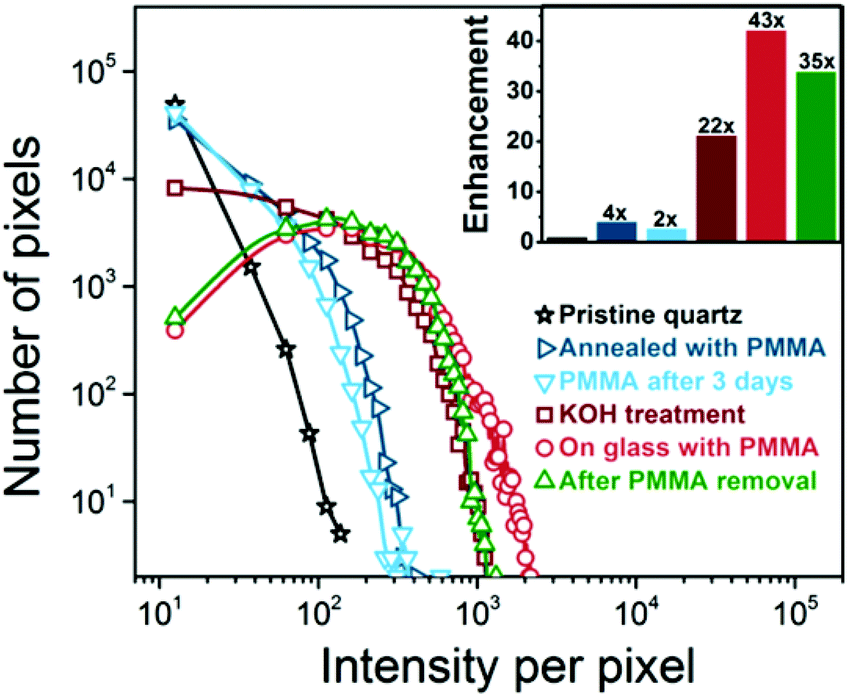 | ||
| Fig. 3 Influence of transfer process steps on PL characteristics: number of pixels versus their PL intensity for SWNT arrays after every transfer process step compared to pristine SWNTs on quartz determined from analysis in the area between the catalyst lines. Inset: corresponding overall intensity enhancement versus pristine SWNTs. | ||
Although PMMA helps in protecting SWNTs from moisture, it is still quite hydrophilic and thus the presence of water cannot be excluded. A more hydrophobic polymer might improve protection from moisture. Covering nanotubes in a PS matrix was previously found to reduce SWNT blinking at low temperatures more than a PMMA matrix,27 but PS has not yet been used as a transfer polymer. Following the same transfer process protocol with some adjustments, we transferred the SWNT arrays to a glass substrate with polystyrene instead of PMMA. As shown in Fig. 4 the corresponding PL enhancement was larger (59-fold versus as-grown SWNTs) compared to the transfer with PMMA. The difference of enhancement was even higher before the PS layer was removed (111-fold versus 43-fold). These differences corroborate the idea that the exclusion of moisture and the hydrophobicity of the transfer polymers play an important role in the overall PL enhancement.
 | ||
| Fig. 4 Impact of transfer polymer on the optical response of SWNTs: (a) number of pixels versus PL intensity for SWNT arrays transferred onto glass using PS and PMMA as transfer polymers, with polymer and after removal of the polymer compared to pristine SWNTs on quartz. (b) Corresponding overall intensity enhancement versus pristine SWNTs. PL intensity maps of SWNT arrays transferred to the glass substrate using (c) PMMA or (d) PS as the transfer polymer. | ||
PL spectra recorded at room temperature for a number of SWNTs along a line perpendicular to the SWNT growth after transfer with PMMA and PS and polymer removal are shown in Fig. 5a and b. Overall the PL peak positions correlate well with the expected E11 transitions of SWNTs with a diameter around 1.2 nm. However, for the PS transfer process emission peaks are generally more narrow with a full width at half maximum (FWHM) as small as 26 meV. Although these values are still broad compared to free-standing SWNTs (FWHM ∼ 9 meV)4 they compare well with polymer-wrapped SWNTs in dispersion28 and indicate longer exciton lifetimes.
 | ||
| Fig. 5 Comparison of hyperspectral images of multiple SWNTs transferred to a glass substrate using (a) PMMA or (b) PS as a transfer polymer (the signal at 1060 nm is due to the glass substrate). Corresponding SEM images of SWNT arrays transferred with (c) PMMA and (d) PS as the polymer matrix. | ||
The higher hydrophobicity of the PS may explain the higher PL yield of transferred SWNTs while it is still present but this effect should be gone when the polymer is completely removed. Nevertheless, the PL enhancement after PS removal is still almost twice as high as for the PMMA transfer. A more detailed analysis of high-resolution scanning electron micrographs of PS-transferred SWNT arrays reveals a large number of kinks and wrinkles. In contrast to that, the PMMA-transferred SWNTs remain quite straight even after transfer (see Fig. 5c and d). Both polymers have similar Young's moduli and are heated above their glass transition temperature during the transfer process. Due to the hydrophobic nature of the polystyrene it delaminates more easily from the KOH-etched quartz and wrinkle and kink formation may take place during this step of the transfer. These kinks seem to be preserved after polymer removal and either allow for segments of SWNTs to not be in touch with the underlying substrate or promote the formation of localized states. These states may lower the probability of mobile excitons to encounter quenching sites, thus effectively increasing their emission efficiency.11,29,30 As the kink size (<200 nm) is far below optical resolution a direct correlation is not possible with the available experimental setup.
The final aspect of the transfer of SWNTs is the release of compressive strain. The as-grown SWNTs are under significant strain due to the large volume reduction of the quartz between the growth (865 °C) and room temperature.31,32 Several studies suggest the influence of strain on the photoluminescence of SWNTs.30,33–35 Thus, we also analysed the strain relief during the transfer process by Raman spectroscopy. The as-grown SWNT arrays show a broad distribution around 1600 cm−1 (see Fig. 6) compared to the expected values of 1592 cm−1 indicating strong compressive strain (∼1.1%).32 After KOH treatment the G+-mode distribution becomes very narrow around 1592 cm−1. No D-band is observed before or after treatment (see Fig. S5, ESI†). The nanotubes appear to have relaxed due to the removal of the substrate interaction. After transfer with PMMA, and even more pronounced after transfer with PS, the G+-mode distribution shifts further to wavenumbers slightly below 1590 cm−1, which may indicate weak tensile strain. The lower wavenumbers for the PS-transferred SWNTs and their broader distribution suggest that the observed kinks could be the origin of this tensile strain. The question remains whether the strain relaxation contributes to the PL enhancement or is simply a concomitant phenomenon. A similar shift of the G+-mode can be found after immersing the as-grown SWNTs in n-methylpyrrolidone (NMP) for 4 hours, similar to a typical photolithography lift-off process. However, the PL does not increase substantially (see the inset in Fig. 6). A simple correlation between the G+-mode shift (strain relaxation) and the PL enhancement can be ruled out.
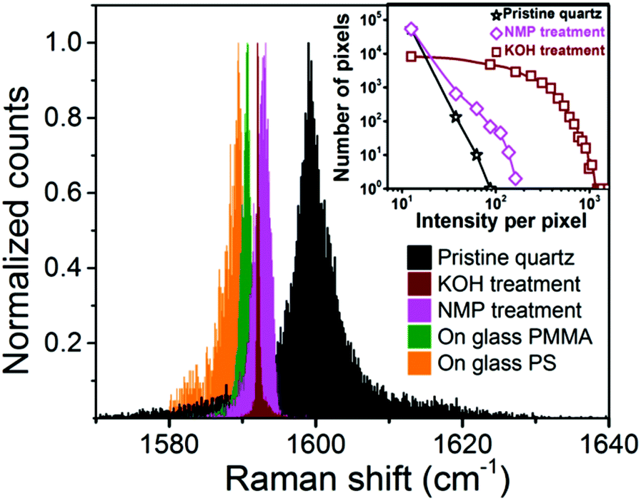 | ||
| Fig. 6 Histogram of G+-mode Raman shifts for pristine SWNT arrays, after etching with KOH (with PMMA), after transfer onto glass with PMMA or PS, and after solvent treatment with NMP only. Inset: number of pixels versus PL intensity for pristine SWNT arrays, after etching with KOH (with PMMA) and after solvent treatment with NMP. | ||
While the presence of a polar substrate such as glass or quartz still lowers the PL efficiency compared to free-standing SWNTs the largest impact seems to be a direct and possibly covalent interaction of the nanotubes with atoms of the quartz surface formed at high temperatures. Soares et al. suggested that non-passivated Si atoms of the quartz could lead to strong interactions between their dangling bonds and the carbon bonding states of the nanotubes.7 Further, the alignment during growth is predominantly caused by angle-dependent van der Waals interactions with the substrate.19 Both interactions can lead to the deformation of the nanotubes, which can affect the band structure even leading to a local reduction or closing of the bandgap and thus metallic segments.7,36,37 After etching of the quartz with KOH these bonds are disrupted and substrate induced deformation of the nanotubes is eliminated. These appear to be the main reasons for enhanced PL. The influence of the polarity of the substrate surface for excitonic decay as discussed by Perebeinos et al.8,9 may contribute but does not seem to be the main quenching source. The additional formation of emissive localized states due to nanotube kinks as discussed for the PS-transferred SWNTs may also contribute.
Conclusions
In summary, we have shown that the photoluminescence of aligned SWNTs grown on quartz can be enhanced by up to two orders of magnitude using a simple polymer transfer process to substrates such as glass or quartz (see Fig. S5, ESI† regarding reproducibility). The PL increase appears to be mostly due to the elimination of the strong SWNT–substrate interactions that directed the growth of the SWNTs. The simple contact with a bare polar substrate or compressive strain after growth does not appear to be the largest quenching sources. Nevertheless, surface water and associated charge-traps for example introduced by oxygen plasma cleaning of the surface should be avoided. Polystyrene as a hydrophobic transfer polymer results in higher PL yields than the more hydrophilic PMMA but less straight SWNTs with numerous kinks, which may be detrimental to charge transport but beneficial for PL yield. These findings can be used as guidelines for improved processing of future light-emitting carbon nanotube devices and demonstrate that the photoluminescence of SWNTs is not insignificant even when in contact with typical polar substrates.Acknowledgements
This research was funded by the Deutsche Forschungsgemeinschaft (DFG) via the Collaborative Research Center “Synthetic Carbon Allotropes” (SFB 953). J. Z. thanks the Alfried Krupp von Bohlen und Halbach-Stiftung via the “Alfried Krupp Förderpreis für junge Hochschullehrer” for general support. Y. Z. acknowledges funding by the European Research Council under the European Union's Seventh Framework Programme (FP/2007–2013)/ERC Grant Agreement No. 306298 (EN-LUMINATE).Notes and references
- L. Xie, C. Liu, J. Zhang, Y. Zhang, L. Jiao, L. Jiang, L. Dai and Z. Liu, J. Am. Chem. Soc., 2007, 129, 12382–12383 CrossRef CAS PubMed.
- L. Ding, D. Yuan and J. Liu, J. Am. Chem. Soc., 2008, 130, 5428–5429 CrossRef CAS PubMed.
- J. Lefebvre, Y. Homma and P. Finnie, Phys. Rev. Lett., 2003, 90, 217401 CrossRef CAS PubMed.
- J. Lefebvre, D. G. Austing, J. Bond and P. Finnie, Nano Lett., 2006, 6, 1603–1608 CrossRef CAS PubMed.
- R. Miura, S. Imamura, R. Ohta, A. Ishii, X. Liu, T. Shimada, S. Iwamoto, Y. Arakawa and Y. K. Kato, Nat. Commun., 2014, 5, 5580 CrossRef CAS PubMed.
- M. S. Hofmann, J. T. Glückert, J. Noé, C. Bourjau, R. Dehmel and A. Högele, Nat. Nanotechnol., 2013, 8, 502–505 CrossRef CAS PubMed.
- J. S. Soares, A. P. M. Barboza, P. T. Araujo, N. M. Barbosa Neto, D. Nakabayashi, N. Shadmi, T. S. Yarden, A. Ismach, N. Geblinger, E. Joselevich, C. Vilani, L. G. Cançado, L. Novotny, G. Dresselhaus, M. S. Dresselhaus, B. R. A. Neves, M. S. C. Mazzoni and A. Jorio, Nano Lett., 2010, 10, 5043–5048 CrossRef CAS PubMed.
- V. Perebeinos and P. Avouris, Phys. Rev. Lett., 2008, 101, 057401 CrossRef PubMed.
- V. Perebeinos, S. V. Rotkin, A. G. Petrov and P. Avouris, Nano Lett., 2009, 9, 312–316 CrossRef CAS PubMed.
- S. Ghosh, S. M. Bachilo, R. A. Simonette, K. M. Beckingham and R. B. Weisman, Science, 2010, 330, 1656–1659 CrossRef CAS PubMed.
- Y. Miyauchi, M. Iwamura, S. Mouri, T. Kawazoe, M. Ohtsu and K. Matsuda, Nat. Photonics, 2013, 7, 715–719 CrossRef CAS.
- Y. Piao, B. Meany, L. R. Powell, N. Valley, H. Kwon, G. C. Schatz and Y. Wang, Nat. Chem., 2013, 5, 840–845 CrossRef CAS PubMed.
- J. J. Crochet, J. G. Duque, J. H. Werner and S. K. Doorn, Nat. Nanotechnol., 2012, 7, 126–132 CrossRef CAS PubMed.
- L. Cognet, D. A. Tsyboulski, J.-D. R. Rocha, C. D. Doyle, J. M. Tour and R. B. Weisman, Science, 2007, 316, 1465–1468 CrossRef CAS PubMed.
- S. J. Kang, C. Kocabas, T. Ozel, M. Shim, N. Pimparkar, M. A. Alam, S. V. Rotkin and J. A. Rogers, Nat. Nanotechnol., 2007, 2, 230–236 CrossRef CAS PubMed.
- S. W. Hong, T. Banks and J. A. Rogers, Adv. Mater., 2010, 22, 1826–1830 CrossRef CAS PubMed.
- M. M. Shulaker, G. Hills, N. Patil, H. Wei, H.-Y. Chen, H.-S. P. Wong and S. Mitra, Nature, 2013, 501, 526–530 CrossRef CAS PubMed.
- C. Kocabas, S.-H. Hur, A. Gaur, M. A. Meitl, M. Shim and J. A. Rogers, Small, 2005, 1, 1110–1116 CrossRef CAS PubMed.
- J. Xiao, S. Dunham, P. Liu, Y. Zhang, C. Kocabas, L. Moh, Y. Huang, K. C. Hwang, C. Lu, W. Huang and J. A. Rogers, Nano Lett., 2009, 9, 4311–4319 CrossRef CAS PubMed.
- H. Wei, Y. Wei, X. Lin, P. Liu, S. Fan and K. Jiang, Nano Lett., 2015, 15, 1843–1848 CrossRef CAS PubMed.
- A. Reina, H. Son, L. Jiao, B. Fan, M. S. Dresselhaus, Z. Liu and J. Kong, J. Phys. Chem. C, 2008, 112, 17741–17744 CrossRef CAS.
- L. Jiao, B. Fan, X. Xian, Z. Wu, J. Zhang and Z. Liu, J. Am. Chem. Soc., 2008, 130, 12612–12613 CrossRef CAS PubMed.
- T. Hallam, N. C. Berner, C. Yim and G. S. Duesberg, Adv. Mater. Interfaces, 2014, 1, 1400115 CrossRef.
- M. Schweiger, M. Schaudig, F. Gannott, M. S. Killian, E. Bitzek, P. Schmuki and J. Zaumseil, Carbon, 2015, 95, 452–459 CrossRef CAS.
- N. Ai, W. Walden-Newman, Q. Song, S. Kalliakos and S. Strauf, ACS Nano, 2011, 5, 2664–2670 CrossRef CAS PubMed.
- C. M. Aguirre, P. L. Levesque, M. Paillet, F. Lapointe, B. C. St-Antoine, P. Desjardins and R. Martel, Adv. Mater., 2009, 21, 3087–3091 CrossRef CAS.
- W. Walden-Newman, I. Sarpkaya and S. Strauf, Nano Lett., 2012, 12, 1934–1941 CrossRef CAS PubMed.
- F. Jakubka, S. P. Schießl, S. Martin, J. M. Englert, F. Hauke, A. Hirsch and J. Zaumseil, ACS Macro Lett., 2012, 1, 815–819 CrossRef CAS.
- C. Georgi, A. A. Green, M. C. Hersam and A. Hartschuh, ACS Nano, 2010, 4, 5914–5920 CrossRef CAS PubMed.
- O. Kiowski, S.-S. Jester, S. Lebedkin, Z. Jin, Y. Li and M. M. Kappes, Phys. Rev. B: Condens. Matter, 2009, 80, 075426 CrossRef.
- L. Ding, W. Zhou, T. P. McNicholas, J. Wang, H. Chu, Y. Li and J. Liu, Nano Res., 2009, 2, 903–910 CrossRef CAS.
- T. Ozel, D. Abdula, E. Hwang and M. Shim, ACS Nano, 2009, 3, 2217–2224 CrossRef CAS PubMed.
- T. K. Leeuw, D. A. Tsyboulski, P. N. Nikolaev, S. M. Bachilo, S. Arepalli and R. Bruce Weisman, Nano Lett., 2008, 8, 826–831 CrossRef CAS PubMed.
- C. D. Spataru and F. Léonard, Phys. Rev. B: Condens. Matter, 2013, 88, 045404 CrossRef.
- P. A. Withey, V. S. M. Vemuru, S. M. Bachilo, S. Nagarajaiah and R. B. Weisman, Nano Lett., 2012, 12, 3497–3500 CrossRef CAS PubMed.
- T. Hertel, R. E. Walkup and P. Avouris, Phys. Rev. B: Condens. Matter, 1998, 58, 13870–13873 CrossRef CAS.
- M. S. C. Mazzoni and H. Chacham, Appl. Phys. Lett., 2000, 76, 1561–1563 CrossRef CAS.
Footnotes |
| † Electronic supplementary information (ESI) available. See DOI: 10.1039/c5nr05163k |
| ‡ Current address: Max Planck Institute for the Science of Light, Günther-Scharowsky-Straße 1, 91058 Erlangen, Germany. |
| This journal is © The Royal Society of Chemistry 2015 |