
 Open Access Article
 This Open Access Article is licensed under a Creative Commons Attribution-Non Commercial 3.0 Unported Licence
Interface formation of two- and three-dimensionally bonded materials in the case of GeTe–Sb2Te3 superlattices†
Jamo
Momand
*a,
Ruining
Wang
b,
Jos E.
Boschker
b,
Marcel A.
Verheijen
c,
Raffaella
Calarco
b and
Bart J.
Kooi
*a
aZernike Institute for Advanced Materials, University of Groningen, Nijenborgh 4, 9747 AG Groningen, The Netherlands. E-mail: j.momand@rug.nl; b.j.kooi@rug.nl
bPaul-Drude-Institut für Festkörperelektronik, Hausvogteiplatz 5-7, 10117 Berlin, Germany
cEindhoven University of Technology, Department of Applied Physics, NL-5600 MB Eindhoven, The Netherlands
First published on 26th October 2015
Abstract
GeTe–Sb2Te3 superlattices are nanostructured phase-change materials which are under intense investigation for non-volatile memory applications. They show superior properties compared to their bulk counterparts and significant efforts exist to explain the atomistic nature of their functionality. The present work sheds new light on the interface formation between GeTe and Sb2Te3, contradicting previously proposed models in the literature. For this purpose [GeTe(1 nm)–Sb2Te3(3 nm)]15 superlattices were grown on passivated Si(111) at 230 °C using molecular beam epitaxy and they have been characterized particularly with cross-sectional HAADF scanning transmission electron microscopy. Contrary to the previously proposed models, it is found that the ground state of the film actually consists of van der Waals bonded layers (i.e. a van der Waals heterostructure) of Sb2Te3 and rhombohedral GeSbTe. Moreover, it is shown by annealing the film at 400 °C, which reconfigures the superlattice into bulk rhombohedral GeSbTe, that this van der Waals layer is thermodynamically favored. These results are explained in terms of the bonding dimensionality of GeTe and Sb2Te3 and the strong tendency of these materials to intermix. The findings debate the previously proposed switching mechanisms of superlattice phase-change materials and give new insights in their possible memory application.
Introduction
Phase-Change Materials (PCMs) based on Ge, Sb and Te (GeSbTe) are some of the most promising candidates for next-generation data-storage applications.1,2 Due to their unique combination of functional properties, they are currently under intense investigation for non-volatile random-access memory. Recently, a new concept of nanostructured PCMs has been developed based on GeTe–Sb2Te3 superlattices, referred to as Interfacial Phase-Change Material or Chalcogenide Superlattice (CSL).3,4 This type of material shows strongly improved switching properties compared to its bulk counterparts, as well as new possibilities for multi-level switching5 and magnetic functionality.6–8 Initially it was proposed that the switching was due to the amorphous-crystalline phase-transition of the separate relatively thick superlattice sublayers, where the improved performance was attributed to the reduced thermal conductivity of the superlattice structure.4,5 However, it was demonstrated that the CSL kept functioning while the GeTe sublayer thickness was narrowed down to ≤1 nm, equivalent to two or three bilayers (BLs) GeTe, and that CSL had higher thermal conductivity compared with bulk GeSbTe. It was concluded that the phase-change occurred within the crystalline state, as was verified with transmission electron microscopy (TEM), not requiring the melt-quench cycle and thereby inherently acquiring improved properties and stability.3Despite these advances, the crystal structure and switching mechanism of CSL is currently not clearly understood. As both GeTe and Sb2Te3 are based on abc-stacking of close-packed atomic planes, with repeating units (Ge-Te-)m and (Te-Sb-Te-Sb-Te-)n, CSL is being modeled for simplicity as (GeTe)2(Sb2Te3)1 with stacking sequences as shown in Fig. 1a. The structure by Kooi et al. corresponds experimentally best to the stable phase of Ge2Sb2Te5![[thin space (1/6-em)]](https://www.rsc.org/images/entities/char_2009.gif) 9 (rhombohedral Ge2Sb2Te5), the prototype conventional PCM, which is consistent with ab initio calculations at zero temperature. However, at elevated temperatures of 180 °C and above these calculations suggest that the Kooi et al. phase becomes progressively unfavorable and therefore the other sequences dominate.8,10,11 Based on these results, two competing switching models were derived, which originate from the understanding of the Ge umbrella-flip mechanism in PCMs.12,13 Tominaga et al. propose that the two phases of CSL correspond to the Ferro low-resistance state and inv. Petrov high-resistance state with a single GeTe umbrella flip as shown in Fig. 1b,8,10 while Ohyanagi et al. propose the Petrov low-resistance state and inv. Petrov high-resistance state with a double GeTe umbrella flip as shown in Fig. 1c.14
9 (rhombohedral Ge2Sb2Te5), the prototype conventional PCM, which is consistent with ab initio calculations at zero temperature. However, at elevated temperatures of 180 °C and above these calculations suggest that the Kooi et al. phase becomes progressively unfavorable and therefore the other sequences dominate.8,10,11 Based on these results, two competing switching models were derived, which originate from the understanding of the Ge umbrella-flip mechanism in PCMs.12,13 Tominaga et al. propose that the two phases of CSL correspond to the Ferro low-resistance state and inv. Petrov high-resistance state with a single GeTe umbrella flip as shown in Fig. 1b,8,10 while Ohyanagi et al. propose the Petrov low-resistance state and inv. Petrov high-resistance state with a double GeTe umbrella flip as shown in Fig. 1c.14
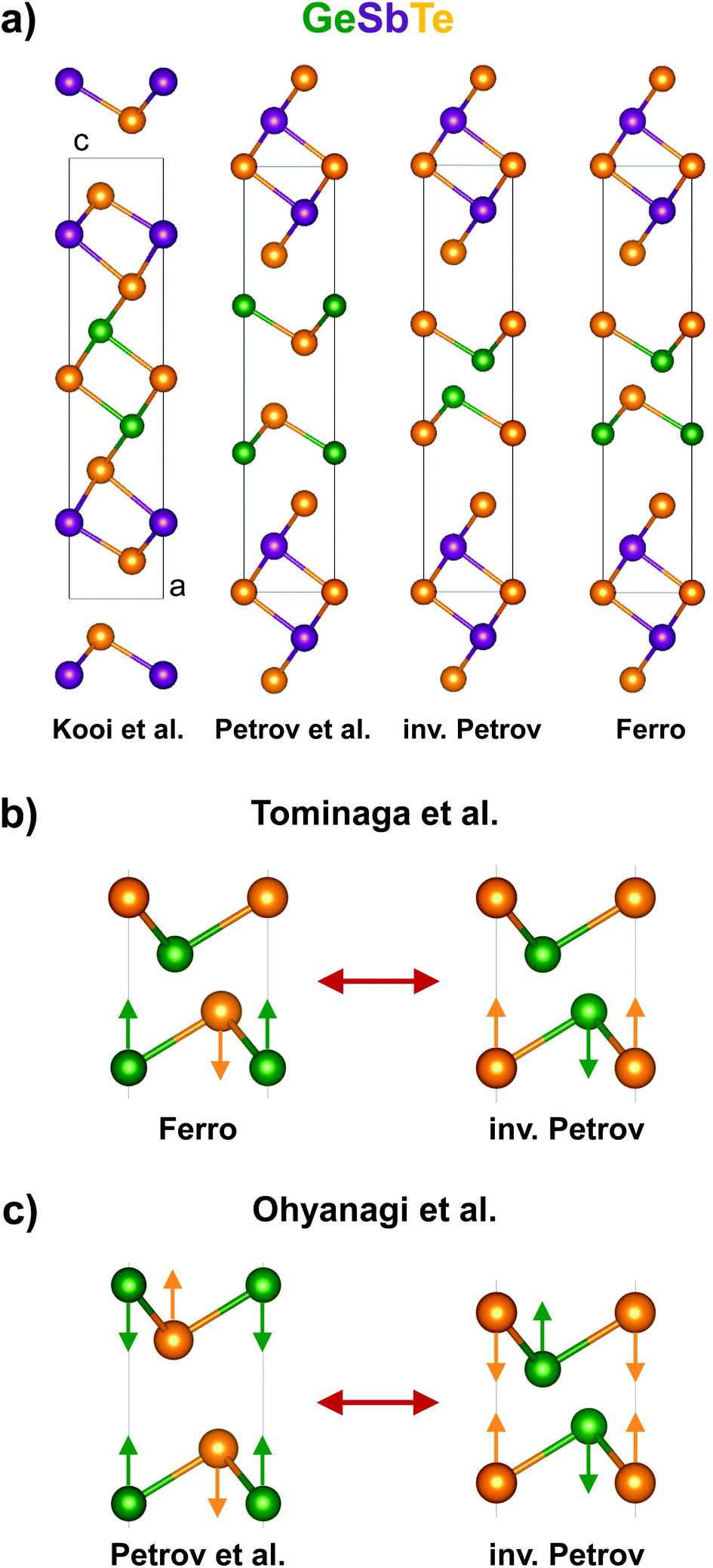 | ||
| Fig. 1 Models of GeTe–Sb2Te3 superlattices considered in the literature. (a) Simple CSL stacking sequences in case of (GeTe)2(Sb2Te3)1; (b) CSL switching model proposed by Tominaga et al. considering a single Ge umbrella flip;8,10 (c) CSL switching model proposed by Ohyanagi et al. considering a double Ge umbrella flip;14 note that in both cases of b and c the switching cannot be the result of only a vertical flip of Ge atoms (because this would disagree with the abc-type stacking).11 | ||
There are several problems with these models that need to be addressed to progress the understanding of CSL operation. Bulk GeTe and Sb2Te3 are three-dimensionally (3D) and two-dimensionally (2D) bonded solids, respectively, where the Te–Te bond of the latter is of van der Waals (vdW) type.15,16 This implies that vdW-surfaces of “entire” quintuple layers (QLs) Sb2Te3, written schematically as (Te-Sb-Te-Sb-Te-vdW-), are passive and do not prefer to bind with dangling bonds of GeTe. In this respect the experimental structure by Kooi et al. best satisfies this condition, as the GeTe BLs are intercalated within the Sb2Te3 block where the bonding is 3D, while the other models do not properly match the GeTe and Sb2Te3 bonding types. Moreover, since it is known from experiments that stable Ge2Sb2Te5 contains mixed Ge/Sb atomic layers,17 lowering the free energy of the PCM at higher temperatures due to configurational entropy, it is debatable whether modelling CSL with pure Ge or Sb atomic planes as in Fig. 1 is justified. Hence, it is not clear why the structures in Fig. 1, other than the experimentally accepted one based on ref. 9 and 17 would be thermodynamically stable, and why, therefore, the proposed switching mechanisms would be correct.
These problems are addressed in the present work, where the previously found switching models of CSL are challenged and an alternative ground state structure is presented. By using highly controlled Molecular Beam Epitaxy (MBE), which has shown in our previous work to produce high-quality Sb2Te315 and GeTe16 thin films and GeSbTe memory devices,18 [GeTe(1 nm)–Sb2Te3(3 nm)]15 superlattices have been grown on the Sb-passivated surfaces of Si(111), (√3 × √3)R30°-Sb, at a substrate temperature of 230 °C as described in Experimental. The crystal structure of the films is resolved using various characterization techniques, including X-Ray Diffraction (XRD), Energy Dispersive X-ray spectroscopy (EDX) and High-Angle Annular Dark Field Scanning Transmission Electron Microscopy (HAADF-STEM). Contrary to the previously proposed models, it is demonstrated that the structure of the films corresponds to van der Waals bonded layers (i.e. a van der Waals heterostructure19) of Sb2Te3 and rhombohedral GeSbTe, in agreement with expectation based on models proposed by Kooi et al.9 and Matsunaga et al.17 Moreover, preliminary memory characterization shows that similar MBE grown films indeed display clear CSL memory behavior with for instance a reduction of the programming current by a factor three in comparison to the same devices containing bulk GeSbTe. The present results therefore indicate that the models for CLS switching as depicted in Fig. 1b and c are unlikely and that a revision of the switching mechanism is required.
Results
The average XRD, XRR and EDX results in the ESI† demonstrate that [GeTe(1 nm)–Sb2Te3(3 nm)]15 has been grown with a clear, well-defined and stoichiometrically consistent superlattice feature. The structure of this CSL is then studied with HAADF-STEM, of which an overview is shown in Fig. 2a. The Si substrate at the bottom of the image appears darker than the film due to Z-contrast and the dark horizontal lines in the film correspond to the vdW type Te–Te bonds, referred to as vdW gaps. Since Sb2Te3 and GeTe have 2D and 3D bonding, respectively,15,16 the formation of vdW gaps is expected to be at least between adjacent QLs of Sb2Te3. The superlattice feature of the film can then be recognized in this image by (i) Z-contrast of Ge with respect to Sb and Te (having approximately equal Z) and (ii) the 2D bonded Sb2Te3 QLs, which are separated by vdW gaps. Hence, the periodicity of the alternating GeTe–Sb2Te3 block is indicated on the left in the figure, pointing each time roughly to the Sb2Te3 sublayers.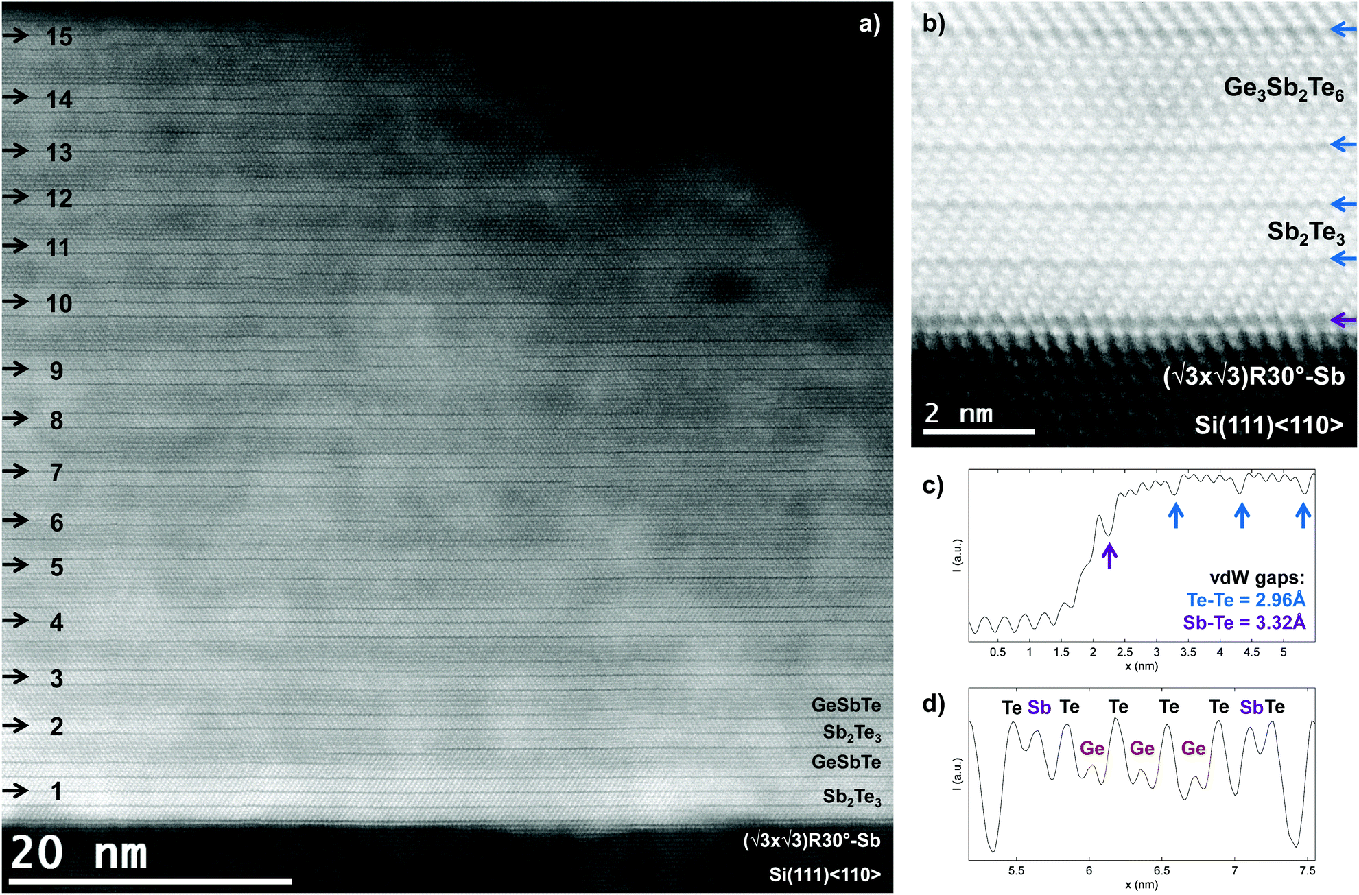 | ||
| Fig. 2 HAADF-STEM measurements on the as-deposited superlattice. (a) Overview micrograph of the [GeTe(1 nm)–Sb2Te3(3 nm)]15 CSL grown by MBE; (b) close-up of the Si(111)–Sb–Sb2Te3 interface and GeSbTe layer formation, which is deduced to be Ge3Sb2Te6 from d; (c) intensity linescan corresponding to the Si(111)–Sb–Sb2Te3 interface in b; (d) intensity linescan corresponding to the GeSbTe layer in b. | ||
Two observations can be made from the overview image in Fig. 2a. First, it is deduced by the number of vdW gaps that typically 1 or 2 instead of the expected 3 QLs Sb2Te3 are formed, where the vdW-layer thicknesses are 1 QL or larger. The reason is that the vdW-layers consist of entire QLs Sb2Te3, while for GeTe rather the formation of (GeTe)n + Sb2Te3 or rhombohedral GeSbTe occurs. This is why almost exclusively vdW layers of odd number atomic planes are formed. Second, various stacking and layering faults are seen in the image, particularly double-plane defects in between the odd-numbered atomic plane vdW layers, which is a consequence of the fact that the film is not perfectly deposited plane by plane. However, the clear occurrence of vdW gaps and their spatial extension affirms the smoothness of growth achieved with MBE, reflecting its high-quality layer by layer growth. Also, twinning and twin-boundaries are observed as the crystal is viewed along Si<1![[1 with combining macron]](https://www.rsc.org/images/entities/char_0031_0304.gif) 0> or Sb2Te3<11
0> or Sb2Te3<11![[2 with combining macron]](https://www.rsc.org/images/entities/char_0032_0304.gif) 0>, where the abc-stacking becomes apparent. From ϕ-scans around the Sb2Te3(220), shown in ESI Fig. S4,† it is found that an approximately equal number of opposite twin-domains exist in the crystal. This is also seen in previous work on the growth of Sb2Te3 and can be attributed to the weak bonding in between the vdW-layers.15
0>, where the abc-stacking becomes apparent. From ϕ-scans around the Sb2Te3(220), shown in ESI Fig. S4,† it is found that an approximately equal number of opposite twin-domains exist in the crystal. This is also seen in previous work on the growth of Sb2Te3 and can be attributed to the weak bonding in between the vdW-layers.15
The high-resolution image of the substrate–film interface is shown in Fig. 2b. From this image it becomes apparent that the substrate and film are crystallographically aligned along the hexagonal basis vectors in these planes. In the corresponding linescan in Fig. 2c the vdW gap and structure formation can be studied in more detail. Since the deposition of the film is initiated by passivating the Si(111)-(7 × 7) surface with (√3 × √3)R30°-Sb, the first bright atomic layer on the substrate is Sb, where each of the trivalent Sb atoms bonds to 3 Si dangling bonds and thereby remove the (7 × 7) surface reconstruction.15 The subsequent surface is then of vdW type and vdW epitaxy20 of Sb2Te3 on Si can be achieved, as evidenced by the subsequent deposition of 3 Sb2Te3 QLs. Interestingly, it is measured from Fig. 2c that the Sb–Te distance at the interface is larger than the Te–Te distances in the film, 0.332 nm and 0.296 nm, respectively. This can be explained by the fact that in Sb2Te3 the atomic planes are close-packed on top of each other and thus the Te–Te atomic planes have a distance of close-packed vdW-bond radii of Te atoms. For the substrate–film interface however, there is the ∼11% lattice mismatch, which impedes the close-packing of Sb–Te. The distance of 0.332 nm is nevertheless smaller than the 0.296/√2/3 = 0.363 nm close-packing factor, indicative of some degree of bonding. Note also that in this respect, where the atomic planes have a close-packed configuration and also do not have interplanar dangling bonds, the vdW gap is a different object than an actual vacancy layer, as sometimes is used without distinction in the literature.
On top of the 3 QLs Sb2Te3 in Fig. 2b an 11-layered vdW structure has been formed of which the corresponding intensity linescan is shown in Fig. 2d. By viewing the HAADF-intensities of the atomic columns in the layer and taking into account that the Te atomic plane is alternated with Sb/Ge atomic planes, it is deduced that the stacking is of the form (Te-Sb-Te-Ge-Te-Ge-Te-Ge-Te-Sb-Te-vdW-). This linescan also demonstrates the atomic precision of the MBE growth by showing that almost pure Ge and Sb atomic planes have been formed during deposition with little intermixing of the Ge/Sb planes, as expected for the alloy.17 Hence, the deposition of 1 nm (or 3 BLs) of GeTe has resulted in the formation of a natural or rhombohedral Ge3Sb2Te6 layer and is labeled accordingly. There is an inherent asymmetry between the beginning and the end of the GeSbTe layer in the superlattice, which can be attributed to the growth direction and thus has a kinetic origin. The formation of the (-vdW-Te-Sb-Te-) stacking sequence is surprising in this respect, as Sb2Te3 growth actually occurs in entire 1 nm QLs.15,21 This shows that during this layered Sb2Te3 growth, after the flux transition from Sb to Ge, the film already has a strong tendency to reconfigure itself to form this type of surface and stacking sequence, rather than forming the proposed (inv.) Petrov or Ferro interfaces in Fig. 1a.
The naturally occurring stacking faults and layering disorder in the deposited superlattice seem inconsistent with the high quality that should be achievable with MBE, but this is another signature that the artificially grown CSL reconfigures into a lower energy state. Moreover, the stacking disorder is quite useful for characterization of different types of structures formed. In this way many different vdW layers can be observed, eliminating the necessity for many depositions and sample analyses. Fig. 3 shows parts of the film where layers of different number of atomic planes are formed, namely 5-, 7-, 9-, 11- and 13-layered vdW systems. Starting from the 5-layered system in Fig. 3a and counting forward, it can be seen that the intensity lowering is particularly happening in the center of the vdW layer, confirming the results described above that pure Ge does not bind near the vdW gaps. The 5-layered system is just a QL Sb2Te3 with equal intensity maxima, while the 7-layered system has a single Ge mixed plane with considerable amount of Sb at the center of the layer. The expected stacking sequences occur for 9-, 11- and 13 layers, where almost pure Ge atomic planes are formed, and they already show evidence for Ge intermixing in the Sb layer near the vdW gap. These findings thus confirm that the vdW gap is formed after the -Te-Sb-Te termination of the stack, such as in Sb2Te3, and that the GeTe is thus intercalated within the Sb2Te3 block, where its 3D bonding is matched. Note that this is in contrast to phases richer in Sb than Sb2Te3 where Sb bilayers are intercalated within the vdW gaps of Sb2Te3.15,22 Hence, the present results lead to the conclusion that the structure of the as-deposited GeTe–Sb2Te3 superlattice is a vdW heterostructure of Sb2Te3 and rhombohedral GeSbTe.
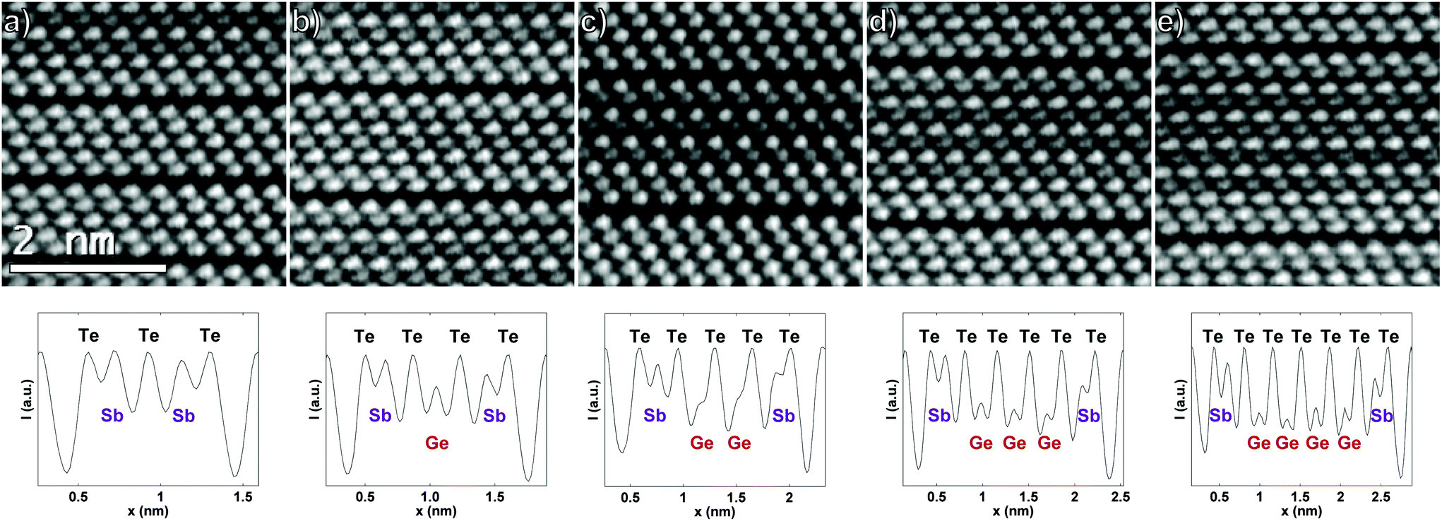 | ||
| Fig. 3 Variety of vdW layers formed in the as-deposited superlattice. The intensity linescans corresponding to the HAADF-STEM micrographs cover larger regions than shown in the representative images. (a) 5-layer; (b) 7-layer; (c) 9-layer; (d) 11-layer; (e) 13-layer; in the linescans the low intensity dips correspond to vdW gaps and the peaks to the Ge, Sb and Te atomic columns. Note that several atomic columns already show evidence of Ge/Sb intermixing. | ||
To monitor the direction of chemical diffusion in the superlattice, another piece of the as-deposited sample has been annealed at 400 °C for 30 min and has undergone the same characterization procedures. A drastic transformation can be observed by comparing XRD acquired on the sample before and after annealing. As shown Fig. 4, after annealing, all the peaks attributed to Sb2Te3 at Qz = 2.4, 3.09, and 4.26 Å−1 disappear and the CSL satellite peak at Qz = 3.46 Å−1, characteristic for the superlattice structure, vanishes as well. The new spectrum displays peaks spaced by ∼0.46 Å−1 which are related (see Fig. 4) to the c lattice parameter of rhombohedral GeSb2Te4 when described with hexagonal axes. These results show that overall Sb2Te3 and GeTe intermix into an ordered GeSb2Te4 structure after annealing and the CSL structure is lost.
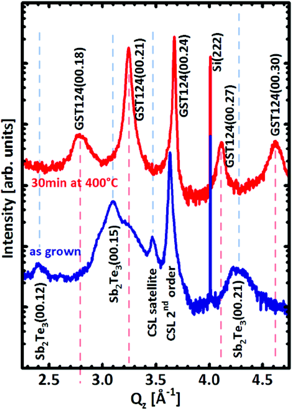 | ||
| Fig. 4 Symmetric 2θ–ω scan on [GeTe(1 nm)–Sb2Te3(3 nm)]15 CSL before (blue line) and after (red line) annealing at 400 °C for 30 min. | ||
The cross-sectional HAADF-micrograph in Fig. 5a shows an overview of the thermally reconfigured film's microstructure, which has retained its layered vdW structure and 2D nature, as is expected for natural GeSbTe.9,17 Interestingly, it is observed that despite the large reconfiguration in the film, the Sb-monolayer terminating the Si substrate has remained intact, reflecting its stability and strong bonding. The Sb2Te3 QLs which were present in the superlattice stack have been dissolved, effectively destroying the superlattice structure, and the remaining film contains primarily 7- and 9-layered vdW systems with thickness of 1.36 ± 0.02 nm and 1.73 ± 0.02 nm, respectively.
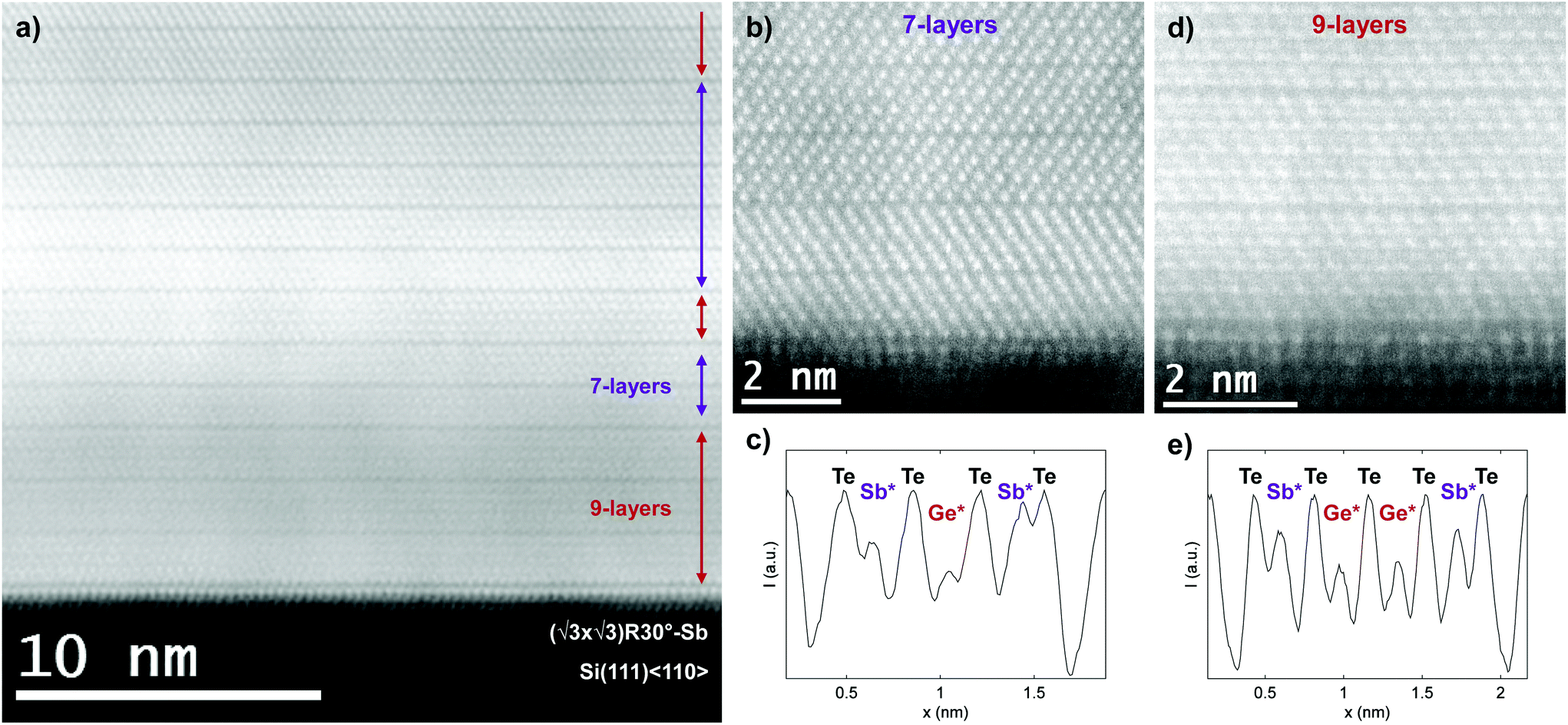 | ||
| Fig. 5 HAADF-STEM measurements on the annealed superlattice. (a) Overview micrograph showing that the CSL has thermally reconfigured into rhombohedral GeSbTe, consisting of 7- and 9-layered vdW blocks; (b) close-up of a region consisting of 7-layered vdW blocks; (c) intensity linescan of a 7-layer shown in b; (d) close-up of a region consisting of 9-layered vdW blocks; (e) intensity linescan of a 9-layer shown in d; the asterisk in c and e indicates that the Ge and Sb atomic planes are intermixed. | ||
Fig. 5b, c and d, e show the formation of 7- and 9-layered structures near the substrate with corresponding linescans, respectively. It is observed that the lowest intensity peaks of these structures, indicated by Ge* and Sb*, are again in the center of the vdW layers. Comparing this structure and the thickness of the vdW layers with literature,9,17 it shows that the superlattice created during growth by the alternating supply of Ge and Sb is reconfigured into bulk rhombohedral GeSbTe through the diffusion of Ge atoms. This result thus shows that the thermodynamically favored state of the system is rhombohedral GeSbTe, rather than the structures in Fig. 1a and suggests even stronger Ge intermixing in the superlattice for higher deposition or annealing temperatures. These findings are thus consistent with the previous results on the as-deposited superlattice, which already showed such driving force. However, due to limited time and temperature during deposition complete transformation to rhombohedral GeSbTe is not possible, but screening of GeTe by -Te-Sb-Te was already achieved. Interestingly, as it is known from TEM-EDX measurements that the average composition, which has not changed after the reconfiguration, corresponds best to GeSb2Te4, the structure does not simply reconfigure to exclusively a 7-layered Kooi et al. structure with pure atomic planes (Te-Sb-Te-Ge-Te-Sb-Te-vdW-). In contrast, the formation of 9 layers supports the conclusion of intermixed Ge and Sb layers, as is observed in the HAADF intensities in Fig. 5c and e. The present results are thus fully consistent with the structure proposed for the first time in ref. 17 for stable Ge2Sb2Te5 containing mixed Ge/Sb atomic layers. They also demonstrate that the models in Fig. 1a which only consider pure Ge and Sb planes cannot be used at elevated temperatures, because they neglect the importance of configurational entropy.
Discussion
The Results section shows that the ground state of the GeTe–Sb2Te3 superlattices is actually a vdW heterostructure of Sb2Te3 and rhombohedral GeSbTe, consistent with the provided reasons in the Introduction. The -Te-Sb-Te vdW layer termination plays an important role in the pinning of vdW gaps, as is also expected and found in related compounds such as GeBiTe.23 This is in striking contradiction with the models proposed in the literature,8,10,14 for which the necessary (inv.) Petrov and Ferro structures do not seem to occur in experiments.In addition, these models can hardly be compatible with actual experimental conditions to grow superlattices such as substrate temperature control and surface roughness. It is known from previous work on bulk GeSbTe that GeTe molecules evaporate from the films between 200 °C and 250 °C during growth,24 narrowing the window of deposition. This is not taken into account in previous experiments14 and could play an important role in CSL growth by determining the average GeSbTe layer thickness. Concerning the ‘roughness’, all CSL memories reported in the literature have been grown with 1 nm GeTe thickness.3,7,8,14 These sublayers are always modelled with 2 GeTe BLs, but this is in fact incorrect, because 1 nm corresponds closely to 3 BLs and it is not clear how the structures and mechanisms generalize with such an increased sublayer thickness. When actual memories would rely very sensitively on having either 2 or 3 GeTe BLs, the whole technology becomes hardly realizable in practice.
Furthermore, the experimental evidence provided for the different states of Fig. 1b and c, based, as in this work, on HAADF-STEM images,7,8 does not include (and even shows inconsistencies with) the Z-contrast in these images. Moreover, these images focused on particularly small regions, making it difficult to analyze and compare the overall film structure. The TEM results in the original work by Simpson et al. on CSL memory switching3 indeed show a crystalline feature of the memory in the state which is indicated high-resistance. However, since it is known that GeSbTe can have the amorphous-crystalline transition in films down to 2 nm (ref. 25) and the images were captured using coherent TEM, which suffers from electron delocalization, it is not clear whether this film is partly or entirely crystalline.
The present findings thus disagree with the proposed switching mechanisms of CSL and debate whether it is proven that CSL switching is a fully crystalline-crystalline transition. On the other hand, the currently proposed ground state structure suggests that CSL switching may possibly be a limiting case of the amorphous-crystalline transition of very thin GeSbTe sublayers sandwiched between Sb2Te3 QLs. However, the thermal conductivity of CSL was measured to be lower than for bulk GeSbTe in the work by Simpson et al.,3 dismissing the explanation by Chong et al.4,5 Hence, another mechanism for the reduced programming current should be responsible for the transition. A possible solution to resolve this issue can still be related to the pronounced interfacial and strain energy effects present in the CSLs. For instance, it has been established that that amorphous-crystalline interfaces may be of lower energy than crystalline–crystalline interfaces under certain energetic considerations,26 which thus would reduce the switching energy for thin GeSbTe sublayers sandwiched between crystalline spacer layers than for bulk GeSbTe. Furthermore, the effect of strain can also play a significant role as can be deduced from the a-lattice parameters of the relevant compounds, aGeTe = 0.417 nm,16,27,28aSb2Te3 = 0.426 nm (ref. 9 and 15) and aGe2Sb2Te5 = 0.422 nm,17,29 which indicate that the thicker the rhombohedral GeSbTe vdW sublayer becomes, the more it changes its constant from aSb2Te3 to aGeTe. Thus, the GeSbTe vdW layer can mismatch to a maximum of ∼2% with the Sb2Te3 matrix, depending on its thickness, adding the strain energy to the overall crystalline layer. Therefore, straining the rhombohedral GeSbTe layer could lower its amorphization energy and the enhanced growth speed can be explained by template growth within the crystalline Sb2Te3 matrix,30 consistent with the crystalline feature of TEM observations.3 If this would be correct, a scheme would emerge to design optimal CSL stacks by introducing thin spacer layers that tailor interfacial energy and introduce sufficiently strained GeSbTe layers to lower the amorphization energy (e.g. by adjusting the GeSbTe layer thickness with proper Sb2Te3/GeSbTe ratio), but not too strained as to facilitate sufficiently fast regrowth. Recently, it was also found that GexTe1−x with x ≪ 0.5 in the superlattice, which thus has Ge vacancies and therefore contains more strain of the crystal, reduced the switching energy compared with its stoichiometric GexTe1−x with x = 0.5 counterpart,31 consistent with the proposed hypothesis.
Conclusions
The present work shows that the ground state of GeTe–Sb2Te3 superlattices is actually a vdW heterostructure of Sb2Te3 and rhombohedral GeSbTe, which is in striking contradiction with the previously proposed models in the literature. These GeSbTe layers are formed due to the bonding dimensionality of the superlattice sublayers, as GeTe prefers to be 3D bonded within the Sb2Te3 block and not adjacent to a vdW gap. Such considerations are not taken into account when modeling superlattice PCM, which explains why the model structures are not observed experimentally. Additionally, the ab initio modeled structures do not address the experimentally established atomic intermixing in Ge/Sb layers, omitting the configurational entropy effects on the free energy. More generally, the present results shed light on the bonding types in PCMs lying on the GeTe–Sb2Te3 tie-line, illustrating e.g. why metastable rock-salt GeSbTe structure reconfigures into the stable rhombohedral GeSbTe structure with Te–Te vdW bonds. This is thermodynamically favorable, which is thus also the driving force behind this crystalline order–disorder transition that changes the overall bonding from 3D to 2D. Also, the degree of vdW bonding in rhombohedral GeSbTe probably depends on the degree of Ge/Sb intermixing adjacent to the Te atomic layer at the vdW gap. An increasing mixing of this layer with Ge will then change the Te–Te bond from a passive vdW gap to an actual vacancy layer with dangling bonds, changing the coupling between adjacent GeSbTe layers and thereby probably affecting thermal and electrical conductivities. Overall the present results thus have important implications for understanding the structures and properties of GeTe–Sb2Te3 based CSLs, which are shown to be technologically relevant vdW heterostructures.Experimental
MBE growth and annealing
The cleaning of the Si substrate, its introduction into the MBE system, and the preparation of the Si(111)-(√3 × √3)R30°-Sb surface are detailed in a previous publication.16 The substrate and cells are brought to the deposition temperature of 227.5 °C for the substrate, T(Ge)base = 1120 °C and T(Ge)tip = 1140 °C for the Ge cell, T(Sb)base = 450 °C and T(Sb)tip = 600 °C for the Sb cell, T(Te)base = 340 °C and T(Te)tip = 476 °C for the Te cell. According to previous flux calibration by XRR measurements on amorphous Ge, Sb, and Te films grown at room temperature, these cell temperatures correspond to a Ge flux of 0.16 nm min−1, a Sb flux of 0.15 nm min−1, and a Te flux of 0.45 nm min−1, for a Ge/Sb/Te flux ratio of ∼2/2/5. During growth, the shutter of the Te cell remained open, while the shutters of the Ge and Sb cells are alternatively opened and closed depending on the desired sublayer. The deposition time for each GeTe sublayer of 1 nm is 200 s, and 400 s for Sb2Te3 sublayers of 3 nm. After the deposition of the 15 repetitions, the sample is cooled down to room temperature, and prior to removal from the MBE chamber, the surface is capped with ∼10 nm of Si3N4 by sputtering in the load-lock to prevent oxidation of the last GeTe sublayer. For the annealing experiment, a rapid thermal annealing (RTA) furnace was used. The annealing was performed on different pieces of the same sample, in less than 1 bar of nitrogen atmosphere. The temperature of 400 °C was reached from RT with a ramp of 10 °C s−1.TEM characterization
Cross-sectional TEM specimen were prepared along the Si(111)<10> substrate crystallographic directions by mechanical polishing, dimple grinding and low-voltage Ar+ ion-milling for final thinning using a Gatan PIPS II. Average EDX measurements were performed on 4 different cross-sectional specimen of the [GeTe–Sb2Te3]15 superlattice using a JEOL 2010 equipped with a LN2-cooled SiLi detector. The spectra were fitted (<1.4% error) with the Cliff–Lorimer (MBTS) correction method w/o absorbance as implemented in the NSS 2.3 software package from Thermo Scientific. HAADF-STEM measurements were carried out using a JEOL ARM200F with sub-Å point resolution settings, where the accelerating voltage was 200 kV, the semi-convergence angle was 22 mrad and ADF collecting angles were 68–280 mrad. Calibration of images is typically performed on the basis of the Si(111) interplanar distance (0.3135 nm). Image analysis was in all cases carried out on raw data using GMS 2.30 software and all linescans in this paper were normalized to the background by dividing them with a highest order unique polynomial through the Te peaks in the vdW layer + 2 neighboring Te peaks outside this layer. For better visibility, micrographs in Fig. 3 and 5a were filtered with the Average Background Subtraction Filter (ABSF) filter,32 freely available at http://www.dmscripting.com/hrtem_filter.html.
XRD and XRR characterization
XRD and XRR characterizations were performed using a PANalytical X'PertTM triple-axis diffractometer with Cu(Kα-1) radiation (λ = 1.540598 Å) and Ge(220) hybrid monochromator. The XRR fits were carried out with the specular interface model of the X'Pert reflectivity fitting software.Visuals
The visuals in Fig. 1 were created using the freely available VESTA software package.33Acknowledgements
This work was supported by EU within the FP7 project PASTRY (GA 317746).References
- G. W. Burr, M. J. Breitwisch, M. Franceschini, D. Garetto, K. Gopalakrishnan, B. Jackson, B. Kurdi, C. Lam, L. A. Lastras, A. Padilla, B. Rajendran, S. Raoux and R. S. Shenoy, J. Vac. Sci. Technol., B, 2010, 28, 223–262 CAS.
- D. Lencer, M. Salinga and M. Wuttig, Adv. Mater., 2011, 23, 2030–2058 CrossRef CAS PubMed.
- R. E. Simpson, P. Fons, A. V. Kolobov, T. Fukaya, M. Krbal, T. Yagi and J. Tominaga, Nat. Nanotechnol., 2011, 6, 501–505 CrossRef CAS PubMed.
- T. C. Chong, L. P. Shi, R. Zhao, P. K. Tan, J. M. Li, H. K. Lee, X. S. Miao, A. Y. Du and C. H. Tung, Appl. Phys. Lett., 2006, 88, 122114 CrossRef.
- T. C. Chong, L. P. Shi, X. Q. Wei, R. Zhao, H. K. Lee, P. Yang and A. Y. Du, Phys. Rev. Lett., 2008, 100, 136101 CrossRef CAS PubMed.
- J. Tominaga, R. E. Simpson, P. Fons and A. V. Kolobov, Appl. Phys. Lett., 2011, 99, 152105 CrossRef.
- D. Bang, H. Awano, J. Tominaga, A. V. Kolobov, P. Fons, Y. Saito, K. Makino, T. Nakano, M. Hase, Y. Takagaki, A. Giussani, R. Calarco and S. Murakami, Sci. Rep., 2014, 4 Search PubMed.
- J. Tominaga, A. V. Kolobov, P. J. Fons, X. Wang, Y. Saito, T. Nakano, M. Hase, S. Murakami, J. Herfort and Y. Takagaki, Sci. Technol. Adv. Mater., 2015, 16, 014402 CrossRef.
- B. J. Kooi and J. T. M. D. Hosson, J. Appl. Phys., 2002, 92, 3584–3590 CrossRef CAS.
- J. Tominaga, A. V. Kolobov, P. Fons, T. Nakano and S. Murakami, Adv. Mater. Interfaces, 2014, 1, 1300027 Search PubMed.
- X. Yu and J. Robertson, Sci. Rep., 2015, 5, 12612 CrossRef CAS PubMed.
- A. V. Kolobov, P. Fons, A. I. Frenkel, A. L. Ankudinov, J. Tominaga and T. Uruga, Nat. Mater., 2004, 3, 703–708 CrossRef CAS PubMed.
- J. Tominaga, P. Fons, A. Kolobov, T. Shima, T. C. Chong, R. Zhao, H. K. Lee and L. Shi, Jpn. J. Appl. Phys., 2008, 47, 5763 CrossRef CAS.
- T. Ohyanagi, M. Kitamura, M. Araidai, S. Kato, N. Takaura and K. Shiraishi, Appl. Phys. Lett., 2014, 104, 252106 CrossRef.
- J. E. Boschker, J. Momand, V. Bragaglia, R. Wang, K. Perumal, A. Giussani, B. J. Kooi, H. Riechert and R. Calarco, Nano Lett., 2014, 14, 3534–3538 CrossRef CAS PubMed.
- R. Wang, J. E. Boschker, E. Bruyer, D. D. Sante, S. Picozzi, K. Perumal, A. Giussani, H. Riechert and R. Calarco, J. Phys. Chem. C, 2014, 118, 29724–29730 CAS.
- T. Matsunaga, N. Yamada and Y. Kubota, Acta Crystallogr., Sect. B: Struct. Sci., 2004, 60, 685–691 CrossRef PubMed.
- J. E. Boschker, M. Boniardi, A. Redaelli, H. Riechert and R. Calarco, Appl. Phys. Lett., 2015, 106, 023117 CrossRef.
- A. K. Geim and I. V. Grigorieva, Nature, 2013, 499, 419–425 CrossRef CAS PubMed.
- A. Koma, Thin Solid Films, 1992, 216, 72–76 CrossRef CAS.
- Y. Jiang, Y. Wang, M. Chen, Z. Li, C. Song, K. He, L. Wang, X. Chen, X. Ma and Q.-K. Xue, Phys. Rev. Lett., 2012, 108, 016401 CrossRef PubMed.
- Y. Takagaki, A. Giussani, J. Tominaga, U. Jahn and R. Calarco, J. Phys.: Condens. Matter, 2013, 25, 345801 CrossRef CAS PubMed.
- C. S. Jung, H. S. Kim, H. S. Im, K. Park, J. Park, J.-P. Ahn, S. J. Yoo, J.-G. Kim, J. N. Kim and J. H. Shim, Nano Lett., 2015, 15, 3923–3930 CrossRef CAS PubMed.
- F. Katmis, R. Calarco, K. Perumal, P. Rodenbach, A. Giussani, M. Hanke, A. Proessdorf, A. Trampert, F. Grosse, R. Shayduk, R. Campion, W. Braun and H. Riechert, Cryst. Growth Des., 2011, 11, 4606–4610 CAS.
- R. E. Simpson, M. Krbal, P. Fons, A. V. Kolobov, J. Tominaga, T. Uruga and H. Tanida, Nano Lett., 2010, 10, 414–419 CrossRef CAS PubMed.
- R. Benedictus, A. Böttger and E. J. Mittemeijer, Phys. Rev. B: Condens. Matter, 1996, 54, 9109–9125 CrossRef CAS.
- A. Giussani, K. Perumal, M. Hanke, P. Rodenbach, H. Riechert and R. Calarco, Phys. Status Solidi B, 2012, 249, 1939–1944 CrossRef CAS.
- J. Goldak, C. S. Barrett, D. Innes and W. Youdelis, J. Chem. Phys., 1966, 44, 3323–3325 CrossRef CAS.
- I. Friedrich, V. Weidenhof, W. Njoroge, P. Franz and M. Wuttig, J. Appl. Phys., 2000, 87, 4130–4134 CrossRef CAS.
- R. E. Simpson, P. Fons, A. V. Kolobov, M. Krbal and J. Tominaga, Appl. Phys. Lett., 2012, 100, 021911 CrossRef.
- N. Takaura, T. Ohyanagi, M. Tai, M. Kinoshita, K. Akita, T. Morikawa, H. Shirakawa, M. Araidai, K. Shiraishi, Y. Saito and J. Tominaga, in Electron Devices Meeting (IEDM), 2014 IEEE International, 2014, pp. 29.2.1–29.2.4 Search PubMed.
- R. Kilaas, J. Microsc., 1998, 190, 45–51 CrossRef.
- K. Momma and F. Izumi, J. Appl. Crystallogr., 2011, 44, 1272–1276 CrossRef CAS.
Footnote |
| † Electronic supplementary information (ESI) available. See DOI: 10.1039/c5nr04530d |
| This journal is © The Royal Society of Chemistry 2015 |