
 Open Access Article
 This Open Access Article is licensed under a Creative Commons Attribution-Non Commercial 3.0 Unported Licence
Stretchable and transparent electrodes based on in-plane structures
Kukjoo
Kim
,
Joohee
Kim
,
Byung Gwan
Hyun
,
Sangyoon
Ji
,
So-Yun
Kim
,
Sungwon
Kim
,
Byeong Wan
An
and
Jang-Ung
Park
*
School of Materials Science and Engineering, Wearable Electronics Research Group, Low-Dimensional Carbon Materials Research Center, Ulsan National Institute of Science and Technology (UNIST), Ulsan 689-798, Republic of Korea. E-mail: jangung@unist.ac.kr
First published on 11th August 2015
Abstract
Stretchable electronics has attracted great interest with compelling potential applications that require reliable operation under mechanical deformation. Achieving stretchability in devices, however, requires a deeper understanding of nanoscale materials and mechanics beyond the success of flexible electronics. In this regard, tremendous research efforts have been dedicated toward developing stretchable electrodes, which are one of the most important building blocks for stretchable electronics. Stretchable transparent thin-film electrodes, which retain their electrical conductivity and optical transparency under mechanical deformation, are particularly important for the favourable application of stretchable devices. This minireview summarizes recent advances in stretchable transparent thin-film electrodes, especially employing strategies based on in-plane structures. Various approaches using metal nanomaterials, carbon nanomaterials, and their hybrids are described in terms of preparation processes and their optoelectronic/mechanical properties. Some challenges and perspectives for further advances in stretchable transparent electrodes are also discussed.
1. Introduction
Beyond the concept of conventional appliances, electronics is rapidly evolving toward a new paradigm of deformable electronics, where electronic devices can be deformed into various shapes. Stretchable electronics, in particular, is the most sophisticated form of deformable electronics in that it involves state-of-the-art technologies developed through the collaboration of various disciplines, ranging from materials science to electrical and mechanical engineering.1–3 Potential products employing stretchable electronics exhibit unprecedented attractive applications that strongly appeal to users. Typical examples include wearable healthcare devices, artificial skin and muscles, human–machine interfaces, stretchable displays, and stretchable batteries.4–10As well described in some excellent previous reports,1,11,12 stretchable conductors, among various components, are one of the most important building blocks of stretchable electronics because electrodes and interconnects occupy a very large area portion of electronic devices, thereby absorbing most of the externally induced physical strains. Imparting optical transparency to stretchable electrodes is particularly important for the realization of stretchable optoelectronics, such as stretchable displays,9,13 photovoltaics,14 touch panels,15 and smart contact lenses.16 However, maintaining acceptable electrical and optical performances under mechanical elongation is not readily achieved even with flexible electrodes because a higher level of deformation is required for stretching or twisting than for bending. Therefore, extensive efforts have been recently dedicated to discovering alternative stretchable transparent electrodes beyond flexible transparent electrodes. In most cases, the stretchability of transparent electrodes is rendered by certain structural configurations rather than by exploiting intrinsic properties of materials. Generally, these structural configurations include out-of-plane and in-plane structures of conducting materials. Three-dimensional wavy, crumpled, or coiled shapes are examples of the out-of-plane structure, whereas two-dimensional percolation networks and mesh-like geometries belong to the in-plane structure.
In this mini review, we focus specifically on stretchable transparent thin-film electrodes based on in-plane configurations. In section 2, we compare two distinctive strategies (i.e., out-of-plane and in-plane structure-based approaches) for the realization of stretchable transparent electrodes. Graphene- and conducting polymer-based electrodes are described to compare the two above-mentioned strategies. In sections 3–5, we elucidate the recent advances in stretchable transparent electrodes based on metal nanowires, metal nanomeshes, carbon nanotubes (CNTs), and some other unique approaches. Lastly, in section 6, we discuss present challenges and future directions for stretchable transparent electrodes.
2. Approaches based on out-of-plane or in-plane structures
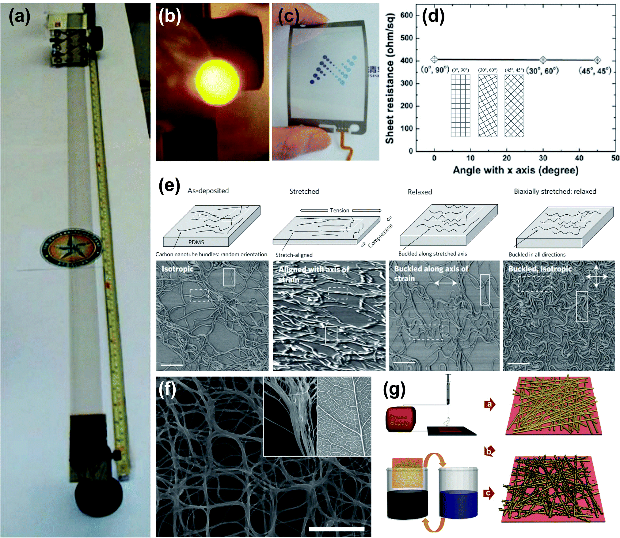
Stretchability of transparent electrodes is usually achieved by structural configurations that accommodate most of the strain under mechanical deformation, thereby rendering little strain to the conducting material itself. These structural configurations can be classified into two approaches: out-of-plane and in-plane structures. The most common out-of-plane structure is the ‘wavy’ structure. The wavy structures can be generally obtained by depositing conductive materials on pre-strained elastomeric substrates, which are subsequently released to allow those conductive films to spontaneously form periodic wavy structures (Fig. 1a).17–19 In this wavy structure, most of the induced strain is absorbed by structural changes (i.e., increased buckling wavelengths and decreased buckling amplitudes), which is similar to accordion bellows. In addition to the simple wavy structures, some other out-of-plane structures have been explored as well, including coiled or spring-like structures.20,21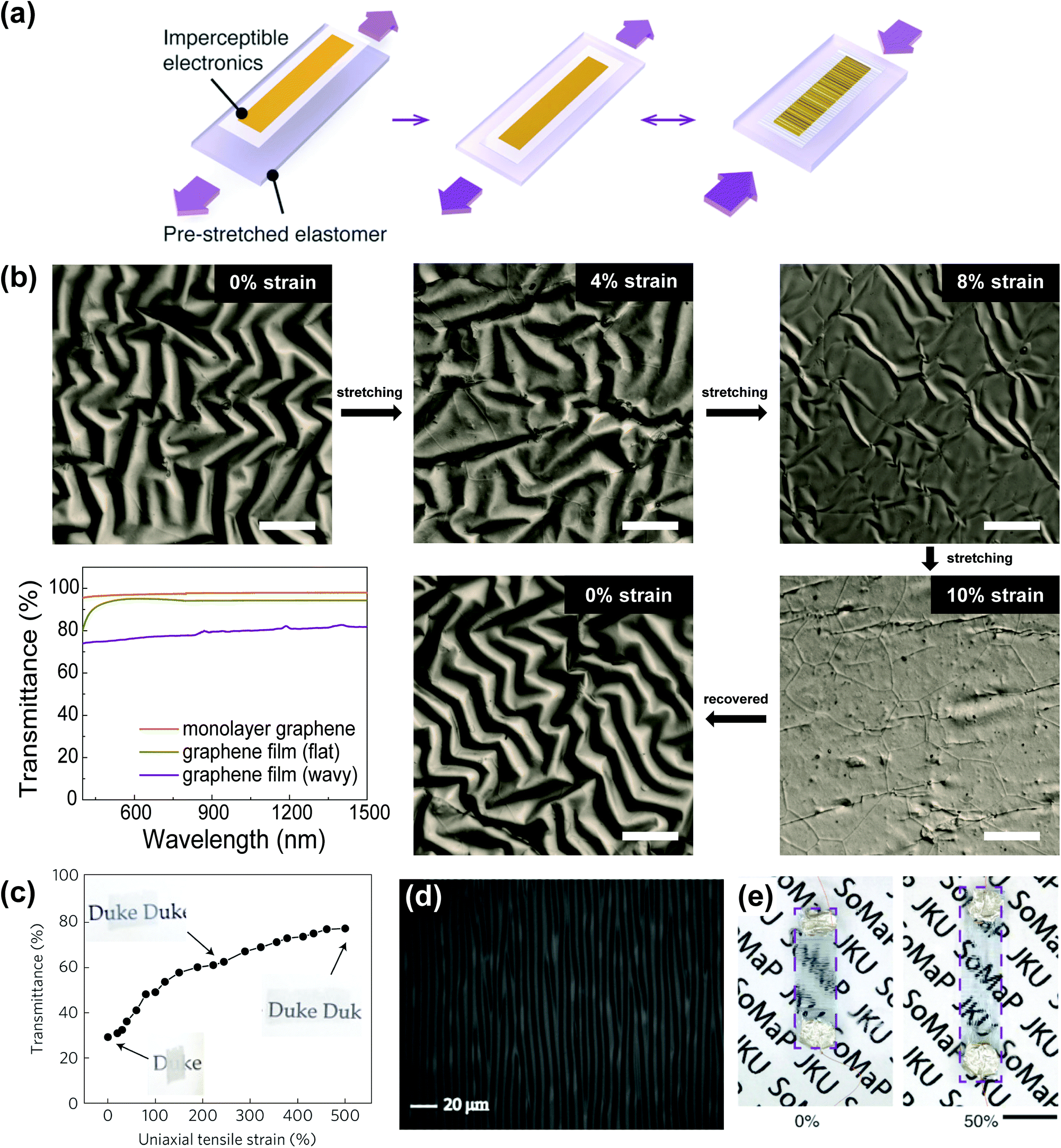 | ||
| Fig. 1 Stretchable transparent electrodes based on out-of-plane structures. (a) Scheme for the preparation of stretchable conductors: the electronic foil is transferred onto a pre-strained elastomer (left, middle) forming out-of-plane wrinkles upon release (right). Reproduced with permission from ref. 17. Copyright 2014, John Wiley and Sons. (b) Total internal reflection fluorescence (TIRF) microscopic images of a wrinkled graphene film during stretching/releasing steps, and corresponding transmittance spectra at stretched and released states (bottom left). All scale bars, 80 μm. (c) Transmittance of the crumpled graphene electrode in the visible range as a function of uniaxial strain. Reproduced with permission from ref. 7. Copyright 2013, Nature Publishing Group. (d) Optical microscopic image of the buckled PEDOT:PSS film (0% strain). Scale bar, 20 μm. Reproduced with permission from ref. 33. Copyright 2011, John Wiley and Sons. (e) Photographs of a translucent wrinkled (left) and transparent flat (right) PEDOT:PSS film. Scale bar, 2 mm. Reproduced with permission from ref. 17. Copyright 2014, John Wiley and Sons. | ||
Graphene is a good example of a stretchable transparent electrode with out-of-plane configuration. Graphene has superior properties, such as high charge carrier mobility, mechanical robustness, chemical stability, and optical transparency and therefore has been investigated in numerous research areas.22–25 Because graphene can be synthesized on large-area templates26 and transferred onto specific substrates,27 many applications have been reported utilizing graphene as electrodes for transistors, supercapacitors, and displays.11 Various flexible devices exploiting the flexibility of graphene have also been demonstrated.28–30 However, despite the superb flexibility of graphene, a stretching-induced tensile strain over 6% causes mechanical failure of graphene due to the fractures within the unique honeycomb structure.27 Thus, the stretchability of graphene electrodes is usually achieved by imparting some structural configurations to graphene films. Recent studies revealed that wrinkled31 or crumpled7 graphene (i.e., graphene films with out-of-plane structures) can endure mechanical deformation, such as bending, distortion, and stretching. Chen et al.31 introduced wrinkled graphene synthesized on a wavy Cu template, showing that wrinkled graphene is able to maintain electrical performances under a strain of up to 40%. Zang et al.7 reported crumpled graphene prepared by transferring graphene onto a polydimethylsiloxane (PDMS) substrate with a pre-strain (εpre) of 400%, followed by the release of the pre-strained elastomer. This crumpled graphene sustained acceptable electrical properties during repeated stretching up to the level of the pre-strain. Such out-of-plane structured graphene films were applied to supercapacitors31 and artificial-muscle actuators.7 We observed the surface morphology change of a wrinkled graphene film, which was deposited on a pre-strained PDMS substrate (εpre = 10%), upon stretching and releasing, as shown in Fig. 1b. As the film stretches from the released state to the fully stretched state (ε = 10%), the film flattens out, becoming almost completely flat at 10% stretching. The graphene film recovers its wrinkled structure upon releasing. This structural change depending on the degree of stretching induces variations in optical transmittance due to light scattering on the surface (the bottom left plot of Fig. 1b), which is unfavourable for transparent electrode applications. Zang et al.7 also reported decreasing transmittance of the crumpled graphene electrode as the pre-strained substrate is released, as shown in Fig. 1c.
Similar to graphene, stretchable transparent electrodes using poly(3,4-ethylenedioxythiophene):poly(styrenesulfonate) (PEDOT:PSS), a representative conducting polymer, have been demonstrated by applying out-of-plane structures to PEDOT:PSS layers. Although PEDOT:PSS has been considered as a promising material for optoelectronics due to its low-cost processability via solution processes, a limited strain sustainability (<5%)32 restricts its use for stretchable electronics without the aid of structural configurations. Lipomi et al.14 successfully demonstrated a stretchable transparent PEDOT:PSS electrode for organic photovoltaics (OPVs) with a buckling structure. The resulting PEDOT:PSS electrode, made on a pre-strained elastomeric substrate, exhibited a stretchability of 20% (up to the pre-strain) with a sheet resistance of 750 Ω sq−1 and transmittance of 96%. Vosgueritchian et al.33 described the use of Zonyl fluorosurfactant to enhance the processability and electrical conductivity of PEDOT:PSS through controlled wettability and phase segregation. A stretchable transparent electrode was fabricated by spin-coating the mixed solution on a pre-strained PDMS substrate (εpre = 15%) and subsequent releasing, providing buckles or waves (Fig. 1d). The resulting electrode showed a sheet resistance of 46 Ω sq−1 with 82% transmittance (measured on a glass substrate) and reversible stretchability, with no change in resistance during 5000 cycles of 10% stretching. A similar approach was introduced by Seol et al.,34 where PEDOT:PSS was mixed with functionalized reduced graphene oxide. The electrode, fabricated by coating this mixture on a pre-strained PDMS substrate, exhibited a sheet resistance of ∼68 Ω sq−1 with 86% transmittance (measured on a glass substrate) and reversible stretchability to the level of pre-strain (ε = 15%).
Further stretchability can be achieved by fabricating devices on ultra-thin polymer substrates, such as 1.4 μm-thick polyethylene terephthalate (PET) films, and laminating them onto a pre-strained elastomer.4,8,17,35 The use of ultra-thin substrates leads to a decreased bending-induced strain within buckles, thereby giving rise to a finer wavy structure upon releasing of the pre-strain, which eventually renders improved stretchability. A PEDOT:PSS transparent electrode adopting this strategy showed excellent stretchability (resistance increased by 30% during 10![[thin space (1/6-em)]](https://www.rsc.org/images/entities/char_2009.gif) 000 cycles of 50% stretching).17
000 cycles of 50% stretching).17
Although the above-mentioned approaches render a high-level of stretchability to graphene and PEDOT:PSS electrodes, the out-of-plane morphology is also accompanied by several undesirable aspects. First, the corrugated or wrinkled out-of-plane structure causes significant light scattering on the surface, which in turn reduces the specular transmittance and raises the haziness of transparent electrodes, as described above (Fig. 1b, c and e). In addition, the direction of stretchability is restricted by those of the pre-strain, while this pre-stretching scheme also presents a challenge for large-area fabrication. Lastly, the change of morphology of electrodes is likely to induce unreliable device operation for different levels of stretching.
Considering the above limitations of out-of-plane approaches, much effort has been dedicated to develop in-plane-structure-based stretchable transparent electrodes. Typical examples of in-plane structures include percolation networks of one-dimensional nanomaterials, such as metal nanowires and CNTs, as well as metal nanomeshes made of ultra-long metal nanofibers or nanotroughs. These entangled web-like structures maintain their conductive pathways even under mechanical deformation owing to the structural reconfiguration through sliding or rotating of nanomaterials against each other. In the following sections, various approaches toward the realization of in-plane-structure-based stretchable transparent electrodes are described. The overall performances of stretchable transparent electrodes based on in-plane structures are summarized in Table 1.
| Materials | Transmittancea | Electrical propertyb | Stretchability | Reliability (cyclic test) | Applications | Ref. |
|---|---|---|---|---|---|---|
| a Transmittance indicates the value at the wavelength of 550 nm, unless otherwise specified. b Electrical property indicates sheet resistance (RS), unless otherwise specified. | ||||||
| Graphene | ∼80% | ∼280 Ω sq−1 | Mechanical failure above ∼6% stretching (without pre-strain) | 3 cycles (ε = ∼6%) | 27 | |
| AgNW (spray coating) | 80% | 35 Ω sq−1 | R S almost unchanged (ε = ∼15%) | LEDs | 53 | |
| AgNW (drop-casting/embedded) | 80% | 88.6 Ω sq−1 | R S < 10 kΩ sq−1 (εmax = 160%) | R S < 2 kΩ sq−1, 5000 cycles (ε = 90%) | Actuators | 54 |
| 45% | 10 Ω sq−1 | |||||
| AgNW (embedded) | 80% | 10 Ω sq−1 | Stable within εmax = 120% | 1000 cycles (ε = 30%) | PLECs | 9 |
| 83% | 15 Ω sq−1 | |||||
| 84% | 25 Ω sq−1 | |||||
| AgNW (drop-casting/embedded) | 90.2% | 50.8 Ω sq−1 | R S (50.8 Ω sq−1) increased by 11.7 times (ε = 33%) | R S increased by 8.5 times, 600 cycles (ε = 50%) | LEDs | 55 |
| 85.1% | 17.5 Ω sq−1 | |||||
| R S (7.5 Ω sq−1) increased by 1.9 times (ε = 33%) | ||||||
| 79.6% | 7.5 Ω sq−1 | |||||
| AgNW (spray coating/embedded) | 80% | 4.5 Ω sq−1 | ΔR/R0 = 32.8% (ε = 100%) | R increased slightly, 50 cycles (ε = 50%) | Photodetectors | 56 |
| AgNW/GO (bar coating) | 88% | 14 Ω sq−1 | Stable within εmax > 100% | 100 cycles (ε = 40%) | PLEDs | 13 |
| 86% | 12 Ω sq−1 | |||||
| AgNW/CNT (solution filtration) | >90% | 24–27 Ω sq−1 | Stable within εmax > 460% (pre-strain: 150%) | LEDs, TSPs | 15 | |
| AgNW/graphene (spin coating) | 94% | 33 Ω sq−1 | Negligible resistance change within ε = 100% | Oxide transistors, single-pixel displays | 16 | |
| AgNW/graphene (spin coating) | 94% | 33 Ω sq−1 | Negligible resistance change within ε = 100% | Negligible resistance change, 10000 cycles (ε = 100%) |
58 | |
| AgNW/graphene (spin coating) | 90% | 25 Ω sq−1 | FET arrays: stable within εmax = 20% | Biosensors | 6 | |
| AgNW/graphene | 80–92% | 98.8 Ω sq−1 | Interactive human–machine interfaces | 57 | ||
| Cu@Cu–Ni NW (embedded) | 80% | 62.4 Ω sq−1 | Resistance increased by 3 times (ε = 20%) | 600 cycles (ε = ∼20%) | OLED circuits | 66 |
| CuNW (embedded) | 91% | 220 Ω sq−1 | Resistance increased twice (ε = 15%) | Resistance increased linearly, 20 cycles (ε = 10%) | 67 | |
| CuNW (embedded) | 84.5% | 56.2 Ω sq−1 | R S < 102 Ω sq−1 (ε = 60%) | Stable up to 200 cycles (ε = 60%) | 68 | |
| 79.5% | 25.0 Ω sq−1 | |||||
| 68.7% | 8.6 Ω sq−1 | |||||
| CuNW (plasmonic welding) | ∼80% | 37 Ω sq−1 | Stable within ε > 250% | R S increased by 10–20%, 800 cycles (ε = 250%) | TSPs | 69 |
| Au nanomesh | 82.5% in the visible range | 21 Ω sq−1 | R S increased by 3.2 times (ε = 160%) | Stable for 1000 cycles (ε = 50%) | 86 | |
| Pt nanomesh | 75.2% | 71 Ω sq−1 | Resistance unchanged (ε = 16.8%) | 89 | ||
| CuNF | 90% | 50 Ω sq−1 | R S: little degradation (ε = 10%) | Solar cells | 63 | |
| AuNF | 81% | 25 Ω sq−1 | R S increased by 56% (ε = 100%) | Resistance unchanged, 1000 cycles (ε = 10%) | Solar cells | 97 |
| PtNF | 90% | 131 Ω sq−1 | R S increased by 10% (ε = 25%) | 98 | ||
| Cu nanotrough | 90% | 2 Ω sq−1 | R S increased by 40% (ε = 50%) | TSPs | 102 | |
| AuNT/graphene | 91% | 1 Ω sq−1 | R S increased by 60% (ε = 80%) | TFTs | 103 | |
| CNT sheets | >85% for perpendicular polarization, >65% for parallel polarization (400–2000 nm) | 755 Ω sq−1 | Resistance increased by ∼6% (ε = 100% with pre-strain of 105%) | First cycle: ΔR/R0 = 6% | OLEDs | 114 |
| Subsequent four cycles: ΔR/R0 < 3% (ε = 100%) | ||||||
| CNT thin films | ∼80% | 1 kΩ sq−1 | ε max = 200% (perpendicular to drawing direction) | Loudspeakers | 115 | |
| SACNT films | 83% | 24 Ω sq−1 | ε max > 120% (perpendicular to drawing direction) | TSPs | 117 | |
| 90% | 208 Ω sq−1 | |||||
| SACNT ribbons/PDMS | 60% (400–800 nm) | 18.8 kΩ | Resistance increased by 1.5 times (ε = 120%) | Stable for 30 cycles (ε = 100%) | 119 | |
| Spring-like SWNT films/PDMS | 79% | 328 Ω sq−1 | Resistance increased by ∼5% (ε = 150%) | Stable for 12500 cycles (ε = 150%) |
120 | |
| Reticulate SWCNT/PDMS | 62% | 53 Ω sq−1 | Resistance increased by 125% (ε = 60%) | Stable for 500 cycles (ε = 40%) | 122 | |
| Porous CNT/PtBa | 77% | 200 Ω sq−1 | Resistance increased by ∼78% (ε = 50%) | ΔR/R0 = 14%, 14 cycles (ε = 40%) | PLECs | 123 |
| SWCNT aerogel/PDMS | 93% (300–1800 nm) | Conductivity: 83 S m−1 | Resistance increased by ∼11% (ε = 100%) | Constant after the fifth cycles (ε = 100%) | 127 | |
| a-SWCNT/PU nanoweb/VHB | 63% | 424 Ω sq−1 | Resistance increased by ∼440% (ε = 100%) | Stable after 6 cycles (ε = 40%) | 130 | |
| Pyrolyzed PDA | 62.6% | 5 kΩ sq−1 (at T = 82.0%) | Resistance increased linearly (ε = 20%) | Stable for 100 cycles (ε = 20%) | Photodetectors | 131 |
| Ag NPs | 70% (400–800 nm) | Conductivity: 2.1 × 10⁶ S m−1 | Electrical failure at ε = 55% | Stable for 900 cycles (ε = 50%) | 132 | |
| Hydrogel-based ionic conductors | 98.9% | Molar conductivity: 120.19 S cm2 mol−1 | Resistance increased with stretch (λ) as R/R0 = λ2 | Actuators, loudspeakers | 133 | |
| Ionogel conductors | 96.95% (380–720 nm) | Conductivity: 0.22 S m−1 | Resistance increased with stretch (λ) as R/R0 = λ2 | Stable for 300 cycles (λ = 4) | Actuators | 134 |
3. Metal nanowires
Stretchable transparent electrodes based on in-plane configurations employing one-dimensional (1D) nanomaterials have attracted much interest with an aim to overcome the abovementioned drawbacks of out-of-plane structure-based stretchable electrodes. 1D nanomaterials with high aspect ratios, such as CNTs and metal nanowires, can organize entangled percolating networks using diverse techniques, including spin coating, spray coating, and drop casting.16,36–39 Among various 1D nanomaterials, metal nanowires have been studied extensively due to their high electrical conductivity and mechanical ductility.3.1. Ag nanowires
Ag is the most widely explored metal in its nanowire form owing to its highest electrical conductivity among various metals.36 Therefore, much effort has been dedicated to deposit Ag nanowires (AgNWs) on various substrates. AgNWs can be synthesized using various methods, such as the hydrothermal method, polyol process, microwave-assisted process, electrochemical technique, UV irradiation technique, and template-assisted technique.40 Prior to the emerging interest in stretchable electronics, AgNW was investigated as a promising material for flexible and transparent electrodes. Early flexible transparent electrodes exploiting AgNWs were fabricated using several techniques, such as vacuum filtration or Meyer rod coating.41,42 These AgNW films were revealed to be thermally/chemically stable, as they maintained good conductivity even after the exposure to heat, water, and organic solvents (e.g., acetone and isopropyl alcohol).42 However, as-prepared AgNW networks on substrates are not favourable in terms of the surface roughness, and hence many studies have reported several methods to improve the roughness, such as the coating of PEDOT:PSS over the percolation network and the embedding of AgNWs into substrates.43–45 These AgNW electrodes with improved roughness were used to demonstrate flexible solar cells and light-emitting diodes (LEDs).43–45 Much effort has also been made to enhance the electrical performances of AgNW films by reducing junction resistance or increasing percolation paths. This has been achieved by employing various welding techniques or by introducing additional materials into the percolation networks.46–52During the improvement of properties and fabrication steps, stretchable transparent electrodes based on AgNWs have been studied at the same time to demonstrate stretchable devices.9,53–56 Akter et al. provided a stretchable AgNW electrode by improving adhesion between a polymer substrate and AgNW networks using poly-dopamine.53 Spray-deposited AgNW electrodes showed excellent properties with a low sheet resistance of 35 Ω sq−1, high transmittance of about 80%, and an unchanged sheet resistance of up to 15% elongation. However, AgNW films that are directly coated on the substrate have undesirable high surface roughness. Alternatively, Pei's group contrived the embedding method where AgNWs are embedded in various polymer substrates, such as poly(tert-butylacrylate-co-acrylic acid), poly(urethane acrylate), and ethoxylated bisphenol A dimethacrylate with aromatic monoacrylate.9,54,55 Adding acrylic acid (AA) into the polymer could improve the interactions between the polymer composite and AgNW networks. Fig. 2a and b show the effective transfer of the AgNWs into the polymer composite using AA. These fabricated transparent and stretchable electrodes were capable of being used for actuators and polymer light-emitting electrochemical cells (PLECs), as shown in Fig. 2c. More recently, Wang et al. reported a surfactant-assisted method using Zonyl fluorosurfactant to reduce the process temperature.56 They demonstrated that the AgNW/PDMS polymer composite with a sheet resistance of 4.5 Ω sq−1 and a transmittance of 80% could stretch up to 100% with resistance increased by 32.8%.
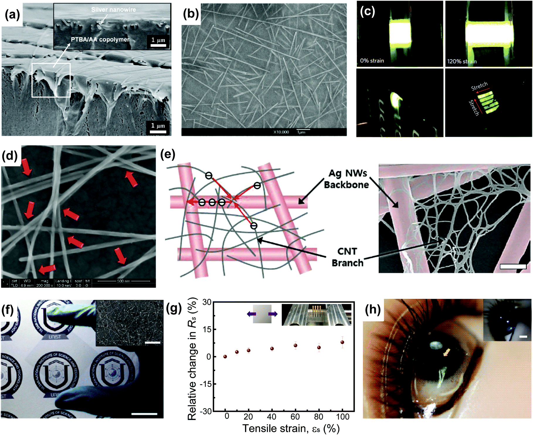 | ||
| Fig. 2 AgNW-based stretchable transparent electrodes. (a) Cross-sectional SEM image of the conductive surface of a AgNW–poly(TBA-co-AA) composite. Scale bar, 1 μm. Reproduced with permission from ref. 54. Copyright 2012, John Wiley and Sons. (b) SEM image of the conductive surface of the AgNW–polymer composite electrodes. Scale bar, 1 μm. Reproduced with permission from ref. 55. Copyright 2012, IOP Publishing. (c) Photographs of PLECs stretched at specified strains and wrapped around the edge of 400 mm-thick cardboard. Reproduced with permission from ref. 9. Copyright 2013, Nature Publishing Group. (d) SEM image of GO-soldered AgNW junctions (indicated by red arrows). Scale bar, 500 nm. Reproduced with permission from ref. 13. Copyright 2014, American Chemical Society. (e) Schematic diagram (left) and SEM image (right) of the hierarchical multiscale AgNW/CNT hybrid nanocomposite for highly stretchable conductors or highly transparent/flexible conductors. Scale bar, 300 nm. Reproduced with permission from ref. 15. Copyright 2014, John Wiley and Sons. (f) Photograph of the graphene–AgNW hybrid film on a PET substrate. Scale bar, 2 cm. The inset shows a SEM image of this hybrid film (scale bar, 5 μm). Reproduced with permission from ref. 16. Copyright 2013, American Chemical Society. (g) The relative difference in the resistance of graphene–AgNW hybrid films on PDMS as a function of tensile strain toward uniaxial direction. Reproduced with permission from ref. 58. Copyright 2015, Springer. (h) Photograph of the ILED/graphene–AgNW hybrid electrode/contact lens device on an eye of a mannequin. (Inset: a photograph for emitting light of the contact lens device on a mannequin eye. Scale bar, 5 mm.) Reproduced with permission from ref. 16. Copyright 2013, American Chemical Society. | ||
The single material of AgNW has clear limitations, such as high inter-nanowire junction resistances, dependence of sheet resistance on pattern sizes, chemical oxidation, and failure due to electrical breakdown. Therefore, the formation of hybrid structures with graphene oxide (GO), CNT, and graphene has been investigated to complement the limitations.6,13,15,16,57,58 As shown in Fig. 2d, the GO–AgNW network fabricated by soaking the AgNW film into the GO dispersion was introduced by Pei's group to reduce the junction resistance without any heat treatment.13 Here, GO flakes provided a soldering effect between crossed AgNWs. This microstructure of the GO–AgNW was applied to a LED with 14 Ω sq−1 sheet resistance and 88% transmittance at 550 nm. The LED still operated even after 100 stretching cycles of 40% strain. More recently, hierarchical multiscale hybrid AgNW/CNT nanocomposites were introduced to achieve a high level of mechanical compliance, conductivity, and transparency, simultaneously.15 In this hierarchical nanocomposite, CNTs wrap the AgNW junctions and prevent the separation of junctions even at harsh stretching conditions. Although this work used the pre-strain method (εpre = 150%), the composite electrode retained its functionality even under a strain of 400%. The schematic and scanning electron microscopy (SEM) images of nanocomposites based on longer (thicker) AgNWs (diameter: ∼150 nm, length: ∼50–100 μm) and shorter (thinner) CNTs (diameter: ∼1.2 nm, length: ∼2–10 μm) are presented in Fig. 2e.
The combination of two-dimensional (2D) nanomaterials, such as graphene with AgNWs has been intensively explored as well. Park's group fabricated stretchable transparent electrodes based on graphene and AgNWs, as shown in Fig. 2f.6,16,58 These hybrid structures achieved high transmittance (94%) and low resistance (33 Ω sq−1), which can be attributed to the increased conducting pathways compared to the electrode consisting solely of AgNWs. Fig. 2g shows that the AgNW/graphene hybrid electrode can be stretched up to 100% with a negligible change in resistance. This hybrid electrode has been applied to various stretchable and transparent electronics, including LEDs (Fig. 2h), biosensors, and human–machine interfaces.6,16,57
3.2. Cu nanowires
Although AgNW-based stretchable transparent electrodes show promising optoelectronic and mechanical characteristics, low availability of natural Ag gives rise to the cost issue, which is critical for mass production. Thus, Cu nanowires (CuNWs) have been rising as an alternative due to their comparable conductivity and flexibility with AgNWs as well as low cost originating from relatively high natural abundance of Cu.11,59 CuNWs can be synthesized using a number of methods, including aqueous reduction of copper salts,60,61 non-aqueous self-catalytic growth62 and electrospinning.63,64 One of the main drawbacks of CuNW-based stretchable transparent electrodes is that they are easily oxidized throughout the growth and device fabrication processes. The oxidation of CuNWs eventually degrades the performance and reliability of devices that adopt CuNW-based electrodes. Therefore, improving the chemical stability is the most urgent subject for successful applications of CuNW-based stretchable transparent electrodes.One method that is known to hamper the oxidation of CuNWs is Ni coating on the surface of CuNWs.65,66 Song et al. reported a stretchable transparent electrode using CuNWs with Cu4Ni alloying shells (Cu@Cu–Ni NWs) embedded in an elastomer substrate, as shown in Fig. 3a.66 This Cu@Cu–Ni NW-based electrode (sheet resistance of 62.4 Ω sq−1 and transmittance of 80%) showed remarkable chemical stability against oxidation in a natural environment for over 30 days while the bare CuNW-based electrode showed resistance increase of 100% after 10 days. The electrode based on Cu@Cu–Ni NWs retained its electrical performance even after cyclic stretching (20%), bending, or twisting.
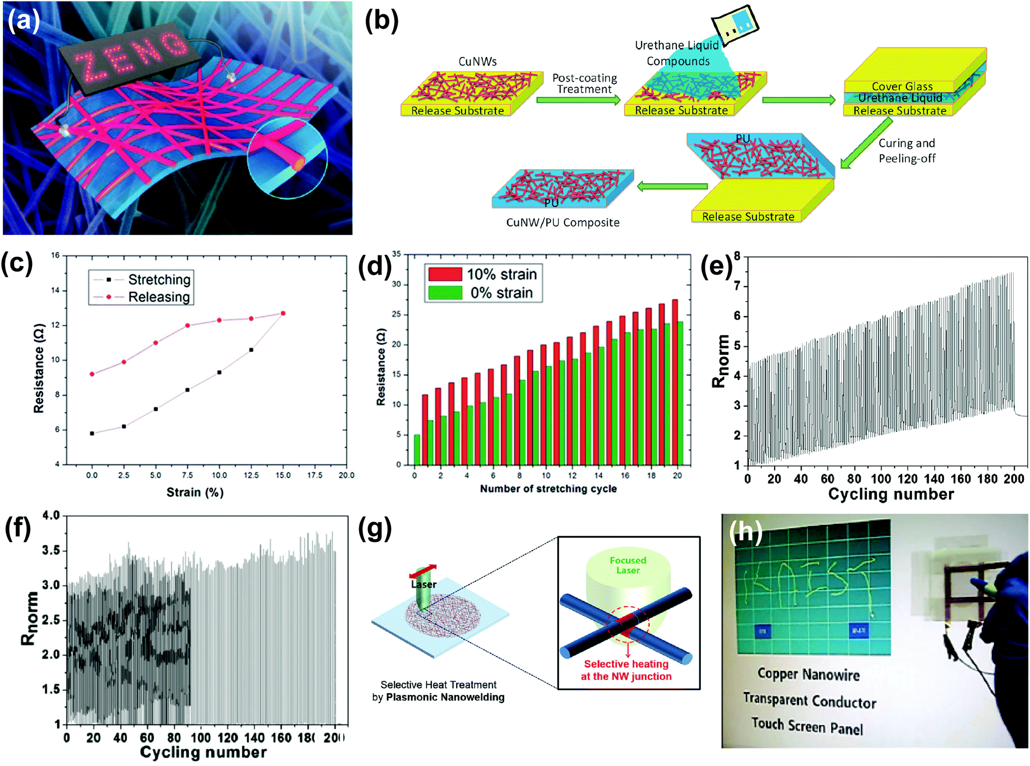 | ||
| Fig. 3 CuNW-based stretchable transparent electrodes. (a) Schematic illustration of Cu@Cu–Ni NWs embedded in an elastomer substrate. Reproduced with permission from ref. 66. Copyright 2014, American Chemical Society. (b) Schematic illustration of the fabrication process of a CuNW–PU composite electrode. Reproduced with permission from ref. 68. Copyright 2013, Royal Society of Chemistry. (c) Resistance change of a CuNW/poly(acrylate) electrode (R0 = 5.8 Ω) during the first stretching and releasing. (d) Resistance change for a 5 Ω CuNW/poly(acrylate) electrode being cycled between 0% and 10% strain for 20 times. (c and d) Reproduced with permission from ref. 67. Copyright 2014, Royal Society of Chemistry. (e and f) Normalized transient resistance of (e) pristine CuNW/PU composite electrodes and (f) 6-aminohexanoic acid pretreated CuNW/PU composite electrodes during the cyclic stretching–releasing process with the peak strain of 40% at the stretching speed of 0.01 mm s−1. (e and f) Reproduced with permission from ref. 68. Copyright 2013, Royal Society of Chemistry. (g) Schematic illustration of the plasmonic laser nanowelding process of CuNWs. (h) Demonstration of the touch-screen panel fabricated with a laser-nanowelded CuNW transparent conductor. (g and h) Reproduced with permission from ref. 69. Copyright 2014, John Wiley and Sons. | ||
However, the Ni coating onto the surface of CuNWs degrades the overall transparency of the resulting electrodes. Thus, several research groups have demonstrated stretchable transparent electrodes using pristine CuNWs where the oxidation was prevented by embedding CuNWs into the polymeric substrates (Fig. 3b).67,68 The polymer matrix not only prevents the oxidation of CuNWs, but also provides intimate contact within the nanowires, which eventually leads to an enhanced durability under stretching. The electrode based on CuNWs partly embedded in the poly(acrylate) substrate exhibited a transmittance of 91% and a sheet resistance of 220 Ω sq−1.67 The resistance increased by about 100% at the rupture strain of ∼15% (Fig. 3c) and showed a linearly increasing tendency for 20 stretching cycles of 15% elongation (Fig. 3d). Pei's group added an additional chemical (6-aminohexanoic acid) to the polymer matrix to prevent the delamination of CuNWs from the polymeric substrate during the stretching.68 The electrode using 6-aminohexanoic acid showed less change in the electrical performance compared to the electrode without 6-aminohexanoic acid at 40% stretching, as shown in Fig. 3e and f.
The conventional thermal annealing process for the welding of the junctions between nanowires also induces the oxidation of CuNWs. To solve this problem, Han et al. reported plasmonic nanowelding of CuNWs (Fig. 3g), which not only improves the sheet resistance of resulting transparent electrodes, but also reduces the oxidation of CuNWs during the welding process.69 The resulting electrode using plasmonic-nanowelded CuNWs exhibited a transmittance of ∼80% at 550 nm and a sheet resistance of 37 Ω sq−1. The electrode transferred onto an Eco-flex film endured a very large strain (>250%) with negligible resistance changes, and it was successfully utilized for a touch screen panel, as shown in Fig. 3h.
According to some previous reports,69–73 welded metal nanowire (AgNW or CuNW) networks also show more stable electrical performance under mechanical deformations than non-welded networks. This can be ascribed to the difference in deformation between non-welded and welded networks. While a non-welded network accommodates strains by rotating and/or sliding of each nanowire against others at the junctions, a welded network accommodates strains by reconfiguring the network structure in the same manner that a fishnet changes its shape when it is stretched. Thus, the junctions in a non-welded network can be easily detached or broken by bending or stretching, whereas the junctions in a welded network firmly connect distinct nanowires even under harsh stretching.
4. Metal nanomeshes
To achieve high quality stretchable transparent electrodes using metal nanowires, defect-free nanowires should be synthesized with conductivities close to those of bulk metals.38,41,52,63,74–76 These refined metal nanowires should then be carefully deposited on a substrate with a density above the percolation threshold to provide sufficient current paths within the percolation networks.77,78 This percolation threshold could be fulfilled more easily if metal nanowires had higher aspect ratios.77 Additionally, ultra-long metal nanowires reduce the dependence of total resistance of transparent electrodes on the junction resistances between nanowires. Based on this idea, alternative nanostructures, such as nanomeshes, nanofibers, and nanotroughs, have been extensively explored to realize stretchable transparent electrodes.4.1. Metal grids
A metal grid with a grating structure is the most basic form of a metal nanomesh for flexible or stretchable transparent electrodes. The transmittance and sheet resistance of metal grids can be controlled using key parameters such as film thickness, grid line width and grid pattern pitch.79,80 To obtain high transmittance (above 90% at 550 nm) and maintain low sheet resistance, the grid line width should be reduced and the grid pattern pitch should be optimized considering the trade-off between sheet resistance and transmittance. In addition to the conventional photolithography,80–82 which requires multiple fabrication steps, including a vacuum process, various fabrication methods have been utilized to demonstrate metal grid electrodes, including inkjet printing,83 electrohydrodynamic inkjet,79,84 direct writing,85 and imprinting.74Although the optoelectronic characteristics of metal grid electrodes can be readily tuned, they only present the stretchability along a diagonal direction to the grating pattern. The elongation of the grating pattern along the orthogonal directions is likely to induce undesired cracks or failure of the electrode. Therefore, metal grids with random or meandering networks have recently been investigated to obtain the stretchability without any directivity. Guo et al. reported a stretchable transparent Au nanomesh electrode using grain boundary lithography.86 This electrode showed a sheet resistance of 21 Ω sq−1 and a transmittance of 82.5%. Also, it can be stretched up to 160% with the sheet resistance increased by 3.2 times. They also reported the recovery effect of Au nanomesh electrodes under cyclic stretching or compression by taking advantage of the cold-welding phenomenon, where welding of damaged parts occurs due to the pressures induced by mechanical deformation,87 thereby providing a durable and generally applicable stretchable transparent electrode.88 Jang et al. reported a hexagonal Pt nanomesh electrode using anodized aluminium oxide (AAO) template as a substrate. Pt was sputtered on an AAO template and then the AAO template was removed, providing a transferable Pt nanomesh with a honeycomb structure.89 This Pt nanomesh electrode showed a sheet resistance of 71 Ω sq−1 with a transmittance of 75.2%, and it could be stretched up to 16.8% without any significant changes in resistance.
4.2. Metal nanofibers and nanotroughs
As mentioned previously, the meandering design90 and smaller line width79,80 are prerequisites for preferable stretchable transparent electrodes. Therefore, conducting random networks with high aspect ratio nanomaterials beyond nanowires are required.91 Based on this idea, metallic nanofibers have been attracting substantial interest as an alternative material for stretchable transparent electrodes. Most metallic nanofibers have been fabricated by electrospinning, which is a facile method to make continuous and long nanofibers from polymeric solutions using electrohydrodynamics.92,93The first attempt to fabricate metallic nanofibers via electrospinning adopted the precursor-based method,63,94–96 where the metal salts (precursors) were dissolved in appropriate solvents, followed by electrospinning of this solution. The polymeric components were then selectively removed by calcination at high temperature. To convert the resulting metal oxide nanofibers to metallic nanofibers, a further reduction process was required. As shown in Fig. 4a, Cui's group fabricated Cu nanofibers (CuNFs) by electrospinning copper acetate dissolved in poly(vinyl acetate).63 The resulting CuNFs had ultrahigh aspect ratios of up to 100000 and fused crossing points with ultralow junction resistances (Fig. 4b), which were utilized for stretchable electrodes with a high transmittance (90%) and a low sheet resistance (50 Ω sq−1). As shown in Fig. 4c, this CuNF-based transparent electrode exhibited negligible conductance degradation after stretching by 10% strain, while the resistance of thin Cu films increased 100 times under the same stretching conditions.
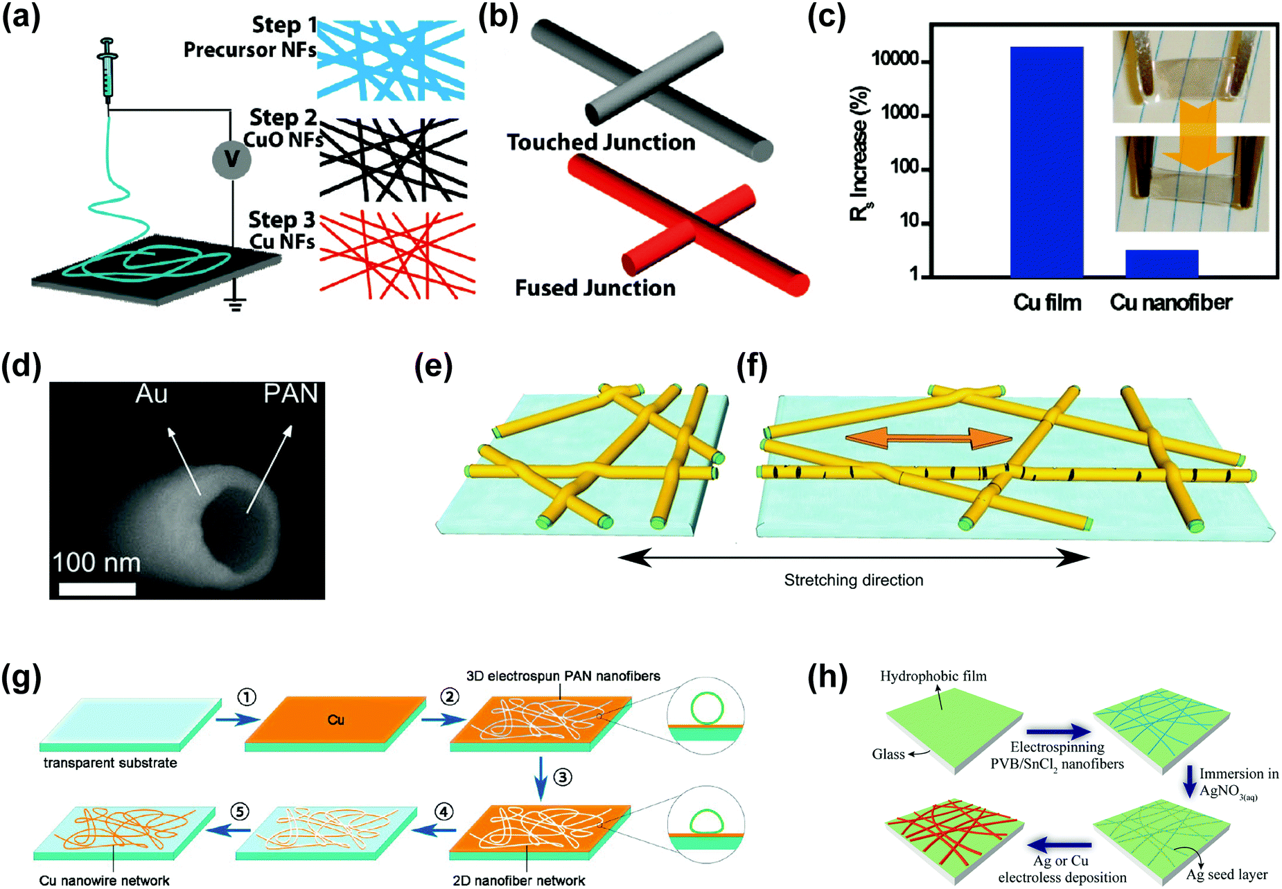 | ||
| Fig. 4 Metal nanofiber-based stretchable transparent electrodes. (a) Schematic illustration of electrospinning of nanofibers. Left column: schematic illustration of an electrospinning setup, shown without a syringe pump. Right column: the fabrication process of Cu nanofibers. (b) Schematic illustration of junctions between solution-processed Ag nanowires (upper) and electrospun Cu nanofibers (down). (c) Cu nanofiber networks with small changes in terms of sheet resistance upon stretching with 10% strain. (a–c) Reproduced with permission from ref. 63. Copyright 2010, American Chemical Society. (d) Cross sectional SEM micrograph of a sparse nanofiber transparent conductor web embedded in an epoxy resin. (e and f) Schematic illustrations of the evolution of the nanofiber web under the applied strain. (d–f) Reproduced with permission from ref. 97. Copyright 2013, John Wiley and Sons. (g) Scheme of Cu nanowire (nanofiber) network electrode fabrication. Reproduced with permission from ref. 99. Copyright 2014, American Chemical Society. (h) Schematic illustration of electroless deposited metallic electrospun nanowire transparent electrodes. Reproduced with permission from ref. 100. Copyright 2014, American Chemical Society. | ||
The electrode prepared by the precursor-based method showed limited flexibility or stretchability due to the coalescence of nanofibers at the intersections and required high-temperature heat treatment for the reduction process. To simplify the fabrication steps of metallic nanofibers, the vacuum deposition method was proposed.97,98 Servati's group demonstrated Au nanofiber (AuNF) networks by sputtering Au onto the electrospun polyacrylonitrile (PAN) nanofiber networks (Fig. 4d), which mimicked the natural fibrous structure.97 The resulting web consisted of a conductive Au shell and a flexible PAN core, exhibiting a transmittance of 81% and a sheet resistance of 25 Ω sq−1. In addition, the PAN/Au nanofiber networks transferred to a PDMS substrate presented 56% increase in resistance and 6% increase in optical transmittance upon 100% stretching. Even at 100% strain, AuNFs were deformed with partial cracks, but without electrical disconnection (Fig. 4e and f). The increased optical transmittance at the stretched state was attributed to the sparse nanofiber networks and wider empty spaces generated by the stretching. Also, the resistance of the electrode remained almost unchanged even after 1000 stretching cycles (ε = 10%).
More recently, for cost reduction and mass production, non-vacuum processes, such as the electroless deposition and the mask template method, have been reported.99–101 Zhu's group reported CuNFs using PAN nanofibers as an etching mask (Fig. 4g).99 Electrospun PAN nanofibers were flattened by solvent vapour annealing to provide intimate contact with the underlying thin Cu film. After the Cu etching and removal of the PAN NFs, a CuNF-based transparent electrode was obtained with a sheet resistance of 24 Ω sq−1 at 92% transmittance. Cui's group reported the fabrication of Ag nanofiber (AgNF) or CuNF networks via the combination of electrospinning and electroless deposition, which is a well-known technique to form metal films at a low cost and a large scale.100 Polyvinyl butyral (PVB)/tin(II) chloride (SnCl2) NFs were first formed by electrospinning, and then immersed in the silver nitrate (AgNO3) aqueous solution to form the Ag seed layer only on the surface of nanofibers. Subsequent metallization via electroless deposition provided AgNF or CuNF networks, achieving a sheet resistance of around 10 Ω sq−1 and a transmittance of 90% (Fig. 4h). These electrodes, however, still exhibited limited flexibility and stretchability due to the coalescence of nanofiber junctions.
In addition to the nanofibers, metal nanotroughs with a concave shape were also reported using a low step coverage metal deposition process, as shown in Fig. 5a.102–104 Cui's group reported a Cu nanotrough-based transparent electrode (Fig. 5b) and demonstrated a flexible touch-screen device (Fig. 5c).102 The electrode had outstanding optoelectronic performance (sheet resistance: ∼2 Ω sq−1, transmittance: 90%) and showed reasonable stretchability (∼40% increase in resistance upon 50% uniaxial tensile strain). Hybrid structures of metal nanotroughs and other nanomaterials (e.g., graphene) were also investigated to resolve several problems of nanotroughs, such as (i) high contact resistance with other layers, (ii) percolation problem associated with the pattern size, and (iii) instability in harsh environments.99,103 Park's group reported Au nanotrough (AuNT)/graphene hybrid structures,103 where graphene served as an auxiliary conducting layer and an anti-oxidation layer as well, as shown in Fig. 5d. With the combination of AuNTs and graphene, the resulting transparent electrode exhibited outstanding electrical characteristics with remarkable uniformity (sheet resistance: 1 ± 0.1 Ω sq−1) at 91% transmittance. Also, this electrode showed less than 60% increase in resistance upon 80% stretching, while the AuNT-only film showed 60% increase in resistance for 50% stretching. A skin-attachable, flexible, and highly transparent thin film transistor backplane was demonstrated using this AuNT/graphene hybrid electrode (Fig. 5e–g).
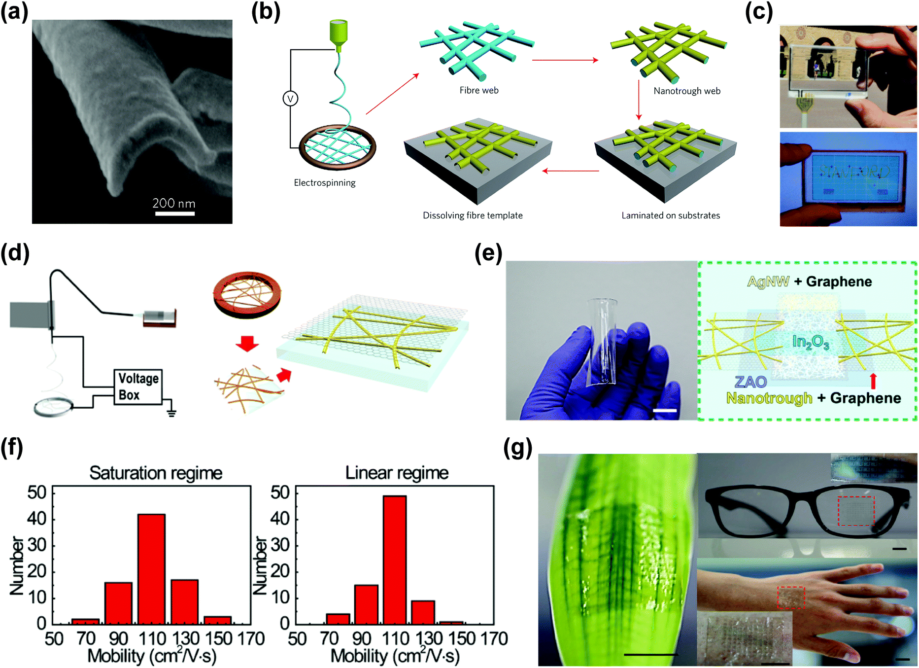 | ||
| Fig. 5 Metal nanotrough-based stretchable transparent electrodes. (a) SEM image of the cross-section of a single Au nanotrough, revealing its concave shape. (b) Schematic illustration of the polymer–nanofiber templating process for fabricating nanotroughs. (c) Photograph of metal nanotrough on a PET film as a transparent electrode for touch screen. (a–c) Reproduced with permission from ref. 102. Copyright 2013, Nature Publishing Group. (d) Schematic images of the processes to form the graphene–metal nanotrough hybrid electrode. (e) A photo (left) of the TFT array sample made by graphene–metal nanotrough hybrid electrodes on a transparent polyimide substrate. Scale bar, 1 cm. A schematic diagram (right) of the TFT layout. (f) Statistical distributions of mobility characteristics of the transistor made by graphene–metal nanotrough hybrid electrodes in linear or saturation regimes. (g) Photographs of the TFT arrays transferred on a leaf, eyeglasses, and the skin of human hand. All scale bars, 1 cm. (d–g) Reproduced with permission from ref. 103. Copyright 2014, American Chemical Society. | ||
5. Other candidates
Apart from the above-mentioned methods, several distinct approaches have been developed for stretchable transparent electrodes, including CNTs, metal nanoparticle-incorporated composites, and hydrogel-based ionic conductors. These unique approaches have diversified the application of stretchable transparent electrodes.5.1. Carbon nanotubes
CNT is one of the most famous allotropes of carbon with a high aspect ratio cylindrical tube shape composed of one or more layers of graphitic carbon (single-walled CNT (SWCNT) or multi-walled CNT).105,106 These cylindrical structures of carbon have remarkable properties, such as high mechanical strength, thermal conductivity, and electrical conductivity.107–109 CNTs can be synthesized using various simple methods, while chemical vapour deposition (CVD), arc discharge, and laser ablation are the most commonly used methods.110–112 Since the initial discovery of the CNT in 1991,105 tremendous number of studies have been conducted on CNTs, owing to its unique properties and relatively simple preparation methods.The early studies on stretchable conductors or electrodes based on CNTs focused on the CNT/polymer composite. CNTs with outstanding mechanical and electrical properties were attractive filler materials blended with a polymer matrix.113 Although CNT/polymer composites were suitable for stretchable conductors, most of them were not optically transparent due to the high concentration of CNT fillers. To expand the usage of stretchable CNT electrodes, many interesting studies have been carried out to improve the optical transparency of CNT-based electrodes.
 | ||
| Fig. 6 CNT-based stretchable transparent electrodes. (a) Photograph of a self-supporting 3.4 cm-wide, meter-long MWNT sheet that has been hand drawn from a nanotube forest at an average rate of 1 m min−1. (b) Photograph of an OLED that uses a solid-state-fabricated aligned MWNT sheet as the hole-injecting electrode. (a and b) Reproduced with permission from ref. 114. Copyright 2005, The American Association for the Advancement of Science. (c) Transparent and flexible touch panels based on SACNT films. Reproduced with permission from ref. 117. Copyright 2010, John Wiley and Sons. (d) Sheet resistance of 4-layer cross-stacked films along the three specific directions indicated in the inset illustration. Reproduced with permission from ref. 118. Copyright 2011, John Wiley and Sons. (e) Evolution of morphology of CNT films with stretching. Schematics (top) and corresponding AFM phase images (bottom) of CNT films. All scale bars, 600 nm. Reproduced with permission from ref. 120. Copyright 2011, Nature Publishing Group. (f) SEM image of the as-grown SWCNT films. Scale bar, 500 nm. The insets show the comparison of the hierarchical reticulate structures of the SWCNT film (left) and the leaf veins (right). Reproduced with permission from ref. 122. Copyright 2012, John Wiley and Sons. (g) Fabrication process of the SWCNT/PU nanoweb to produce a transparent, elastic conductor. Reproduced with permission from ref. 130. Copyright 2012, Royal Society of Chemistry. | ||
Based on a previous report,115 where CNT sheets drawn from a short height of the CNT forest had no large bundles and achieved high transmittance, Feng et al.117 reported highly transparent and roll-to-roll processable superaligned CNT (SACNT) films by reducing the height of the CNT forest and removing residual large bundles in SACNT films with plasma and laser trimming, respectively. Oxygen plasma effectively reduced the height of a SACNT array, and laser trimming removed the outermost CNTs of large bundles from as-drawn SACNT films. In addition, to achieve better electrical conductivity, metals (Au or Ag) were deposited onto the SACNT film, which then exhibited excellent optoelectronic performances with sheet resistances and transmittances of 208 Ω sq−1 at 90% or 24 Ω sq−1 at 83.4%, respectively. The same research group then reported a cross-stacked structure of SACNT films to solve the anisotropy, as shown in Fig. 6d. The resulting SACNT film could be stretched up to 35% along a diagonal direction relative to the stacking angle.118
Despite the above-mentioned interesting progress in the aligned CNT approach, the transparent electrodes made of aligned CNTs showed incomplete stretchability in that they undergo irreversible plastic deformation upon a tensile strain.118 Several strategies to solve this problem were demonstrated by embedding aligned CNTs into the elastomeric matrix.118,119 The resulting electrode exhibited nearly unchanged resistance (35.5 ± 0.3 kΩ) after 6 cycles of 100% stretching.119
Another approach was also demonstrated with a composite of a porous SWCNT three-dimensional (3D) network and elastomer. Yu et al.123 reported the fabrication of nanoporous SWCNT network–polymer composites by Meyer rod coating124 and in situ UV curing of tert-butyl acrylate. This electrode showed a transmittance of >77% and a sheet resistance of 200 Ω sq−1, which increased by 78% under a 50% tensile strain. It was utilized as both the anode and cathode for PLECs. Another interesting method to fabricate porous SWCNT 3D networks was also reported, where ultralight and electrically conducting SWCNT aerogels were prepared by the freeze-drying method.125,126 SWCNT aerogel-based PDMS composites were obtained through the penetration of PDMS into the porous SWCNT aerogel.127 This highly stretchable and transparent (maximum ε = 250% and T = 90%) electrodes showed no significant changes in resistance after 20 cycles of 100% stretching.
Electrospun nanofiber-assisted SWCNT–polymer nanoweb has been emerging as another strategy to obtain random SWCNT network-based electrodes. CNTs can effectively form well-connected conducting networks without agglomeration by simple drop-casting on a well-distributed polymer nanofiber scaffold.128,129 Kim et al.130 also created an acid-treated SWCNT network on web-shaped polyurethane nanofibers through simple electrospinning and dip-coating methods, as shown in Fig. 6g. Utilizing the stretching–releasing method, stretchable electrodes with noodle-like structures were achieved, which exhibited a sheet resistance of 424 Ω sq−1 at 63% transmittance and sustained stable conductivity after 6 cycles of 100% stretching.
5.2. Other approaches for stretchable transparent electrodes
Besides metal nanomaterials and CNTs, several unconventional strategies have been developed to realize stretchable transparent electrodes, such as bio-inspired fabrication of stretchable carbon films,131 polymer gel/metal nanoparticle composites,132 and hydrogel-based ionic conductors.133,134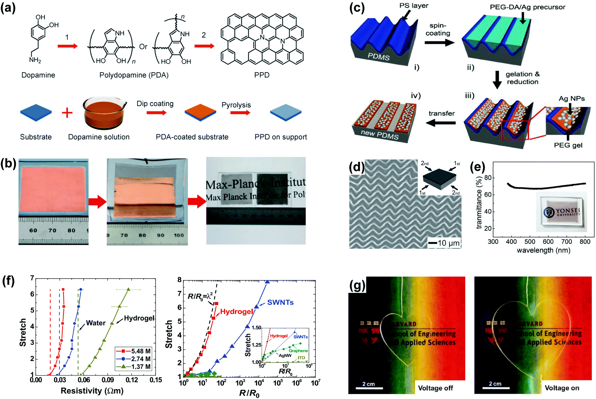 | ||
| Fig. 7 Other approaches for stretchable transparent electrodes. (a) Chemical structures of dopamine, PDA, and pyrolyzed PDA (PPD), and the procedures for the synthesis of PPD film. (1) Self-polymerization. (2) Pyrolysis at elevated temperature. (b) Procedures of the “direct dry-transfer” method and a photograph of PPD films of different transmittances transferred to PDMS sheets by the “direct dry-transfer” method. (a and b) Reproduced with permission from ref. 131. Copyright 2013, John Wiley and Sons. (c) Schematic illustration of the procedure for fabricating highly stretchable, conductive polymer gel/metal nanoparticle composite lines. (d) Polymer gel/metal nanoparticle composite lines prepared from an ordered zigzag buckling generated by sequentially releasing the 2D strains. (e) Transmission spectrum and photograph showing good transparency of the composite electrode in the visible region. (c–e) Reproduced with permission from ref. 132. Copyright 2011, John Wiley and Sons. (f) Electrical resistivities (left) of hydrogels of several concentrations of NaCl as functions of stretch and compared with the resistivities of water containing the same concentrations of NaCl. Stretch versus normalized resistance (right) for ITO, AgNWs, graphene, SWNTs, and hydrogel. (g) Transparent (to all colours) and stretchable actuator using ionic conductor. (f and g) Reproduced with permission from ref. 133. Copyright 2013, The American Association for the Advancement of Science. | ||
Although the hydrogel-based ionic conductor described above can be obtained in a low-cost manner, it is not suitable for applications in open air because hydrogels dry out as water evaporates. To avoid this issue, Chen et al.134 developed an ionogel in which an elastic polymer network hosted a conducting ionic liquid. The volatility of the ionogel was assessed and compared to that of a hydrogel by measuring the weight loss in a thermostatic chamber held at 100 °C. The ionogel showed a weight loss of 12.43% within 12 h while the hydrogel showed a weight loss of 93.69% within 1 h. The conductivity of the ionogel was 0.22 ± 0.01 S m−1 with a transmittance of 96.95%, and the resistance increased proportionally to the square of ‘stretch (λ),’ just like the hydrogel-based one.
6. Concluding remarks
We have witnessed surprising advances in stretchable electronics over the past decade. As an essential component for stretchable electronics, stretchable transparent thin-film electrodes have progressed remarkably, as summarized in this mini review. Metal nanomaterials, such as nanowires, nanofibers, and nanotroughs, exhibit promising characteristics even under high-level mechanical deformation. Also, CNTs and other unique approaches increase the number of feasible options for stretchable transparent electrodes.Stretchable transparent electrodes based on in-plane configurations, however, still require further improvement in several aspects. First, the preparation of high-quality and defect-free nanomaterials should be further refined for acceptable functionalities of electrodes thereof. The chemical stability (e.g., stability against oxidation) of these nanomaterials also needs to be enhanced to guarantee the reliable long-term operation of resulting devices in practical uses. The hybridization of nanomaterials (e.g., AgNWs + graphene) has proven feasible by combining the strengths and compensating the weaknesses of each material, and should be further investigated by exploiting various materials and hierarchical structures. In addition to the material itself, adhesion and interfacial interactions of stretchable transparent electrodes with elastomeric substrates and other constituting active components should be considered as well for the durable operation of final products. Lastly, scalable and low-temperature fabrication processes depending on the materials should be developed in a low-cost manner to facilitate the advent of practical stretchable electronics.
We are now about to see a great leap of electronics towards stretchable form where conventional constraints from rigid form-factors no longer matter. Tremendous research efforts over the past decade have revealed a cornucopia of stretchable electronics with regard to research opportunities and potential applications. Unprecedented applications employing stretchable electronics, including biomedical, healthcare, and wearable devices, are expected to emerge and change our ways of life in the near future.
Acknowledgements
This work was supported by the Ministry of Science, ICT & Future Planning and the Ministry of Trade, Industry and Energy of Korea through Basic Science Research Program of National Research Foundation (2013R1A2A2A01068542), Materials Original Technology Program (10041222), Technology Innovation Program (Grant 10044410), Convergence Technology Development Program for Bionic Arm (NRF-2014M3C1B2048198), and Pioneer Research Center Program (NRF-2014M3C1A3001208). Also, the authors thank Samsung Display and financial support by the Development Programs of Manufacturing Technology for Flexible Electronics with High Performance (SC0970) funded by Korea Institute of Machinery and Materials and by Development of Interconnect System and Process for Flexible Three Dimensional Heterogeneous Devices funded by MOTIE in Korea.Notes and references
- J. A. Rogers, T. Someya and Y. Huang, Science, 2010, 327, 1603–1607 CrossRef CAS PubMed.
- T. Sekitani and T. Someya, Adv. Mater., 2010, 22, 2228–2246 CrossRef CAS PubMed.
- D.-H. Kim and J. A. Rogers, Adv. Mater., 2008, 20, 4887–4892 CrossRef CAS.
- M. Kaltenbrunner, T. Sekitani, J. Reeder, T. Yokota, K. Kuribara, T. Tokuhara, M. Drack, R. Schwödiauer, I. Graz, S. Bauer-Gogonea, S. Bauer and T. Someya, Nature, 2013, 499, 458–463 CrossRef CAS PubMed.
- J. Kim, M. Lee, H. J. Shim, R. Ghaffari, H. R. Cho, D. Son, Y. H. Jung, M. Soh, C. Choi, S. Jung, K. Chu, D. Jeon, S.-T. Lee, J. H. Kim, S. H. Choi, T. Hyeon and D.-H. Kim, Nat. Commun., 2014, 5, 5747 CrossRef CAS PubMed.
- J. Kim, M.-S. Lee, S. Jeon, M. Kim, S. Kim, K. Kim, F. Bien, S. Y. Hong and J.-U. Park, Adv. Mater., 2015, 27, 3292–3297 CrossRef CAS PubMed.
- J. Zang, S. Ryu, N. Pugno, Q. Wang, Q. Tu, M. J. Buehler and X. Zhao, Nat. Mater., 2013, 12, 321–325 CrossRef CAS PubMed.
- M. S. White, M. Kaltenbrunner, E. D. Głowacki, K. Gutnichenko, G. Kettlgruber, I. Graz, S. Aazou, C. Ulbricht, D. A. M. Egbe, M. C. Miron, Z. Major, M. C. Scharber, T. Sekitani, T. Someya, S. Bauer and N. S. Sariciftci, Nat. Photonics, 2013, 7, 811–816 CrossRef CAS.
- J. Liang, L. Li, X. Niu, Z. Yu and Q. Pei, Nat. Photonics, 2013, 7, 817–824 CrossRef CAS.
- S. Xu, Y. Zhang, J. Cho, J. Lee, X. Huang, L. Jia, J. A. Fan, Y. Su, J. Su, H. Zhang, H. Cheng, B. Lu, C. Yu, C. Chuang, T. Kim, T. Song, K. Shigeta, S. Kang, C. Dagdeviren, I. Petrov, P. V. Braun, Y. Huang, U. Paik and J. A. Rogers, Nat. Commun., 2013, 4, 1543 CrossRef PubMed.
- S. Yao and Y. Zhu, Adv. Mater., 2015, 27, 1480–1511 CrossRef CAS PubMed.
- T. Cheng, Y. Zhang, W.-Y. Lai and W. Huang, Adv. Mater., 2015, 27, 3349–3376 CrossRef CAS PubMed.
- J. Liang, L. Li, K. Tong, Z. Ren, W. Hu, X. Niu, Y. Chen and Q. Pei, ACS Nano, 2014, 8, 1590–1600 CrossRef CAS PubMed.
- D. J. Lipomi, B. C.-K. Tee, M. Vosgueritchian and Z. Bao, Adv. Mater., 2011, 23, 1771–1775 CrossRef CAS PubMed.
- P. Lee, J. Ham, J. Lee, S. Hong, S. Han, Y. D. Suh, S. E. Lee, J. Yeo, S. S. Lee, D. Lee and S. H. Ko, Adv. Funct. Mater., 2014, 24, 5671–5678 CrossRef CAS.
- M.-S. Lee, K. Lee, S.-Y. Kim, H. Lee, J. Park, K.-H. Choi, H.-K. Kim, D.-G. Kim, D.-Y. Lee, S. Nam and J.-U. Park, Nano Lett., 2013, 13, 2814–2821 CrossRef CAS PubMed.
- M. Drack, I. Graz, T. Sekitani, T. Someya, M. Kaltenbrunner and S. Bauer, Adv. Mater., 2015, 27, 34–40 CrossRef CAS PubMed.
- D.-H. Kim, J. Xiao, J. Song, Y. Huang and J. A. Rogers, Adv. Mater., 2010, 22, 2108–2124 CrossRef CAS PubMed.
- W. M. Choi, J. Song, D.-Y. Khang, H. Jiang, Y. Y. Huang and J. A. Rogers, Nano Lett., 2007, 7, 1655–1663 CrossRef CAS PubMed.
- Y. Shang, X. He, Y. Li, L. Zhang, Z. Li, C. Ji, E. Shi, P. Li, K. Zhu, Q. Peng, C. Wang, X. Zhang, R. Wang, J. Wei, K. Wang, H. Zhu, D. Wu and A. Cao, Adv. Mater., 2012, 24, 2896–2900 CrossRef CAS PubMed.
- F. Xu, W. Lu and Y. Zhu, ACS Nano, 2011, 5, 672–678 CrossRef CAS PubMed.
- K. S. Novoselov, A. K. Geim, S. V. Morozov, D. Jiang, Y. Zhang, S. V. Dubonos, I. V. Grigorieva and A. A. Firsov, Science, 2004, 306, 666–669 CrossRef CAS PubMed.
- A. K. Geim and K. S. Novoselov, Nat. Mater., 2007, 6, 183–191 CrossRef CAS PubMed.
- K. S. Novoselov, V. I. Fal′ko, L. Colombo, P. R. Gellert, M. G. Schwab and K. Kim, Nature, 2012, 490, 192–200 CrossRef CAS PubMed.
- F. Bonaccorso, Z. Sun, T. Hasan and A. C. Ferrari, Nat. Photonics, 2010, 4, 611–622 CrossRef CAS.
- S. Bae, H. Kim, Y. Lee, X. Xu, J.-S. Park, Y. Zheng, J. Balakrishnan, T. Lei, H. Ri Kim, Y. I. Song, Y.-J. Kim, K. S. Kim, B. Ozyilmaz, J.-H. Ahn, B. H. Hong and S. Iijima, Nat. Nanotechnol., 2010, 5, 574–578 CrossRef CAS PubMed.
- K. S. Kim, Y. Zhao, H. Jang, S. Y. Lee, J. M. Kim, K. S. Kim, J.-H. Ahn, P. Kim, J.-Y. Choi and B. H. Hong, Nature, 2009, 457, 706–710 CrossRef CAS PubMed.
- T.-H. Han, Y. Lee, M.-R. Choi, S.-H. Woo, S.-H. Bae, B. H. Hong, J.-H. Ahn and T.-W. Lee, Nat. Photonics, 2012, 6, 105–110 CrossRef CAS.
- J.-H. Ahn and B. H. Hong, Nat. Nanotechnol., 2014, 9, 737–738 CrossRef PubMed.
- S.-K. Lee, H. Y. Jang, S. Jang, E. Choi, B. H. Hong, J. Lee, S. Park and J.-H. Ahn, Nano Lett., 2012, 12, 3472–3476 CrossRef CAS PubMed.
- T. Chen, Y. Xue, A. K. Roy and L. Dai, ACS Nano, 2014, 8, 1039–1046 CrossRef CAS PubMed.
- J.-H. Ahn and J. H. Je, J. Phys. D: Appl. Phys., 2012, 45, 103001 CrossRef.
- M. Vosgueritchian, D. J. Lipomi and Z. Bao, Adv. Funct. Mater., 2012, 22, 421–428 CrossRef CAS.
- Y. G. Seol, T. Q. Trung, O.-J. Yoon, I.-Y. Sohn and N.-E. Lee, J. Mater. Chem., 2012, 22, 23759–23766 RSC.
- M. Kaltenbrunner, M. S. White, E. D. Głowacki, T. Sekitani, T. Someya, N. S. Sariciftci and S. Bauer, Nat. Commun., 2012, 3, 770 CrossRef PubMed.
- C. Yang, H. Gu, W. Lin, M. M. Yuen, C. P. Wong, M. Xiong and B. Gao, Adv. Mater., 2011, 23, 3052–3056 CrossRef CAS PubMed.
- A. R. Madaria, A. Kumar and C. Zhou, Nanotechnology, 2011, 22, 245201 CrossRef PubMed.
- V. Scardaci, R. Coull, P. E. Lyons, D. Rickard and J. N. Coleman, Small, 2011, 7, 2621–2628 CrossRef CAS PubMed.
- J.-Y. Lee, S. T. Connor, Y. Cui and P. Peumans, Nano Lett., 2008, 8, 689–692 CrossRef CAS PubMed.
- D. Langley, G. Giusti, C. Mayousse, C. Celle, D. Bellet and J.-P. Simonato, Nanotechnology, 2013, 24, 452001 CrossRef PubMed.
- S. De, T. M. Higgins, P. E. Lyons, E. M. Doherty, P. N. Nirmalraj, W. J. Blau, J. J. Boland and J. N. Coleman, ACS Nano, 2009, 3, 1767–1774 CrossRef CAS PubMed.
- L. Hu, H. S. Kim, J.-Y. Lee, P. Peumans and Y. Cui, ACS Nano, 2010, 4, 2955–2963 CrossRef CAS PubMed.
- L. Yang, T. Zhang, H. Zhou, S. C. Price, B. J. Wiley and W. You, ACS Appl. Mater. Interfaces, 2011, 3, 4075–4084 CAS.
- W. Gaynor, G. F. Burkhard, M. D. McGehee and P. Peumans, Adv. Mater., 2011, 23, 2905–2910 CrossRef CAS PubMed.
- Z. Yu, Q. Zhang, L. Li, Q. Chen, X. Niu, J. Liu and Q. Pei, Adv. Mater., 2011, 23, 664–668 CrossRef CAS PubMed.
- J. Lee, P. Lee, H. Lee, D. Lee, S. S. Lee and S. H. Ko, Nanoscale, 2012, 4, 6408–6414 RSC.
- J. Lee, P. Lee, H. B. Lee, S. Hong, I. Lee, J. Yeo, S. S. Lee, T.-S. Kim, D. Lee and S. H. Ko, Adv. Funct. Mater., 2013, 23, 4171–4176 CrossRef CAS.
- Y. Liu, Q. Chang and L. Huang, J. Mater. Chem. C, 2013, 1, 2970–2974 RSC.
- L. Li, J. Liang, S.-Y. Chou, X. Zhu, X. Niu, Z. Yu and Q. Pei, Sci. Rep., 2014, 4, 4307 Search PubMed.
- H. Guo, N. Lin, Y. Chen, Z. Wang, Q. Xie, T. Zheng, N. Gao, S. Li, J. Kang, D. Cai and D.-L. Peng, Sci. Rep., 2013, 3, 2323 Search PubMed.
- I. K. Moon, J. I. Kim, H. Lee, K. Hur, W. C. Kim and H. Lee, Sci. Rep., 2013, 3, 1112 Search PubMed.
- E. C. Garnett, W. Cai, J. J. Cha, F. Mahmood, S. T. Connor, M. Greyson Christoforo, Y. Cui, M. D. McGehee and M. L. Brongersma, Nat. Mater., 2012, 11, 241–249 CrossRef CAS PubMed.
- T. Akter and W. S. Kim, ACS Appl. Mater. Interfaces, 2012, 4, 1855–1859 CAS.
- S. Yun, X. Niu, Z. Yu, W. Hu, P. Brochu and Q. Pei, Adv. Mater., 2012, 24, 1321–1327 CrossRef CAS PubMed.
- W. Hu, X. Niu, L. Li, S. Yun, Z. Yu and Q. Pei, Nanotechnology, 2012, 23, 344002 CrossRef PubMed.
- J. Wang, C. Yan, W. Kang and P. S. Lee, Nanoscale, 2014, 6, 10734–10739 RSC.
- S. Lim, D. Son, J. Kim, Y. B. Lee, J.-K. Song, S. Choi, D. J. Lee, J. H. Kim, M. Lee, T. Hyeon and D.-H. Kim, Adv. Funct. Mater., 2015, 25, 375–383 CrossRef CAS.
- M.-S. Lee, J. Kim, J. Park and J.-U. Park, Nanoscale Res. Lett., 2015, 10, 1–9 CrossRef CAS PubMed.
- L. Hu, H. Wu and Y. Cui, MRS Bull., 2011, 36, 760–765 CrossRef CAS.
- A. R. Rathmell, S. M. Bergin, Y.-L. Hua, Z.-Y. Li and B. J. Wiley, Adv. Mater., 2010, 22, 3558–3563 CrossRef CAS PubMed.
- Y. Chang, M. L. Lye and H. C. Zeng, Langmuir, 2005, 21, 3746–3748 CrossRef CAS PubMed.
- D. Zhang, R. Wang, M. Wen, D. Weng, X. Cui, J. Sun, H. Li and Y. Lu, J. Am. Chem. Soc., 2012, 134, 14283–14286 CrossRef CAS PubMed.
- H. Wu, L. Hu, M. W. Rowell, D. Kong, J. J. Cha, J. R. McDonough, J. Zhu, Y. Yang, M. D. McGehee and Y. Cui, Nano Lett., 2010, 10, 4242–4248 CrossRef CAS PubMed.
- M. Bognitzki, M. Becker, M. Graeser, W. Massa, J. H. Wendorff, A. Schaper, D. Weber, A. Beyer, A. Gölzhäuser and A. Greiner, Adv. Mater., 2006, 18, 2384–2386 CrossRef CAS.
- A. R. Rathmell, M. Nguyen, M. Chi and B. J. Wiley, Nano Lett., 2012, 12, 3193–3199 CrossRef CAS PubMed.
- J. Song, J. Li, J. Xu and H. Zeng, Nano Lett., 2014, 14, 6298–6305 CrossRef CAS PubMed.
- Y. Cheng, S. Wang, R. Wang, J. Sun and L. Gao, J. Mater. Chem. C, 2014, 2, 5309–5316 RSC.
- W. Hu, R. Wang, Y. Lu and Q. Pei, J. Mater. Chem. C, 2014, 2, 1298–1305 RSC.
- S. Han, S. Hong, J. Ham, J. Yeo, J. Lee, B. Kang, P. Lee, J. Kwon, S. S. Lee, M.-Y. Yang and S. H. Ko, Adv. Mater., 2014, 26, 5808–5814 CrossRef CAS PubMed.
- P. Lee, J. Lee, H. Lee, J. Yeo, S. Hong, K. H. Nam, D. Lee, S. S. Lee and S. H. Ko, Adv. Mater., 2012, 24, 3326–3332 CrossRef CAS PubMed.
- J. Lee, J. Y. Woo, J. T. Kim, B. Y. Lee and C.-S. Han, ACS Appl. Mater. Interfaces, 2014, 6, 10974–10980 CAS.
- J. Y. Woo, K. K. Kim, J. Lee, J. T. Kim and C.-S. Han, Nanotechnology, 2014, 25, 285203 CrossRef PubMed.
- X. Ho, C. K. Cheng, J. N. Tey and J. Wei, J. Mater. Res., 2014, 29, 2965–2972 CrossRef CAS.
- M.-G. Kang, M.-S. Kim, J. Kim and L. J. Guo, Adv. Mater., 2008, 20, 4408–4413 CrossRef CAS.
- J. van de Groep, P. Spinelli and A. Polman, Nano Lett., 2012, 12, 3138–3144 CrossRef CAS PubMed.
- D.-S. Leem, A. Edwards, M. Faist, J. Nelson, D. D. C. Bradley and J. C. de Mello, Adv. Mater., 2011, 23, 4371–4375 CrossRef CAS PubMed.
- R. M. Mutiso, M. C. Sherrott, A. R. Rathmell, B. J. Wiley and K. I. Winey, ACS Nano, 2013, 7, 7654–7663 CrossRef CAS PubMed.
- S. De, P. J. King, P. E. Lyons, U. Khan and J. N. Coleman, ACS Nano, 2010, 4, 7064–7072 CrossRef CAS PubMed.
- Y. Jang, J. Kim and D. Byun, J. Phys. D: Appl. Phys., 2013, 46, 155103 CrossRef.
- D. S. Ghosh, T. L. Chen and V. Pruneri, Appl. Phys. Lett., 2010, 96, 041109 CrossRef.
- Y. Zhu, Z. Sun, Z. Yan, Z. Jin and J. M. Tour, ACS Nano, 2011, 5, 6472–6479 CrossRef CAS PubMed.
- Q. Zhang, X. Wan, F. Xing, L. Huang, G. Long, N. Yi, W. Ni, Z. Liu, J. Tian and Y. Chen, Nano Res., 2013, 6, 478–484 CrossRef CAS.
- J.-A. Jeong, J. Kim and H.-K. Kim, Sol. Energy Mater. Sol. Cells, 2011, 95, 1974–1978 CrossRef CAS.
- J. Kang, Y. Jang, Y. Kim, S.-H. Cho, J. Suhr, B. H. Hong, J.-B. Choi and D. Byun, Nanoscale, 2015, 7, 6567–6573 RSC.
- B. Y. Ahn, D. J. Lorang and J. A. Lewis, Nanoscale, 2011, 3, 2700–2702 RSC.
- C. F. Guo, T. Sun, Q. Liu, Z. Suo and Z. Ren, Nat. Commun., 2014, 5, 3121 Search PubMed.
- Y. Lu, J. Y. Huang, C. Wang, S. Sun and J. Lou, Nat. Nanotechnol., 2010, 5, 218–224 CrossRef CAS PubMed.
- C. F. Guo, Y. Lan, T. Sun and Z. Ren, Nano Energy, 2014, 8, 110–117 CrossRef CAS.
- H. Y. Jang, S.-K. Lee, S. H. Cho, J.-H. Ahn and S. Park, Chem. Mater., 2013, 25, 3535–3538 CrossRef CAS.
- K. L. Lin, J. Chae and K. Jain, IEEE Trans. Adv. Packag., 2010, 33, 592–601 CrossRef.
- T. Araki, J. Jiu, M. Nogi, H. Koga, S. Nagao, T. Sugahara and K. Suganuma, Nano Res., 2013, 7, 236–245 CrossRef.
- A. Greiner and J. H. Wendorff, Angew. Chem., Int. Ed., 2007, 46, 5670–5703 CrossRef CAS PubMed.
- D. Li and Y. Xia, Adv. Mater., 2004, 16, 1151–1170 CrossRef CAS.
- J. Kim, J. Kang, U. Jeong, H. Kim and H. Lee, ACS Appl. Mater. Interfaces, 2013, 5, 3176–3181 CAS.
- P.-C. Hsu, H. Wu, T. J. Carney, M. T. McDowell, Y. Yang, E. C. Garnett, M. Li, L. Hu and Y. Cui, ACS Nano, 2012, 6, 5150–5156 CrossRef CAS PubMed.
- M. M. Munir, H. Widiyandari, F. Iskandar and K. Okuyama, Nanotechnology, 2008, 19, 375601 CrossRef PubMed.
- S. Soltanian, R. Rahmanian, B. Gholamkhass, N. M. Kiasari, F. Ko and P. Servati, Adv. Energy Mater., 2013, 3, 1332–1337 CrossRef CAS.
- Y.-K. Fuh and L.-C. Lien, Nanotechnology, 2013, 24, 055301 CrossRef PubMed.
- T. He, A. Xie, D. H. Reneker and Y. Zhu, ACS Nano, 2014, 8, 4782–4789 CrossRef CAS PubMed.
- P.-C. Hsu, D. Kong, S. Wang, H. Wang, A. J. Welch, H. Wu and Y. Cui, J. Am. Chem. Soc., 2014, 136, 10593–10596 CrossRef CAS PubMed.
- K. Azuma, K. Sakajiri, H. Matsumoto, S. Kang, J. Watanabe and M. Tokita, Mater. Lett., 2014, 115, 187–189 CrossRef CAS.
- H. Wu, D. Kong, Z. Ruan, P.-C. Hsu, S. Wang, Z. Yu, T. J. Carney, L. Hu, S. Fan and Y. Cui, Nat. Nanotechnol., 2013, 8, 421–425 CrossRef CAS PubMed.
- B. W. An, B. G. Hyun, S.-Y. Kim, M. Kim, M.-S. Lee, K. Lee, J. B. Koo, H. Y. Chu, B.-S. Bae and J.-U. Park, Nano Lett., 2014, 14, 6322–6328 CrossRef CAS PubMed.
- B. Deng, P.-C. Hsu, G. Chen, B. N. Chandrashekar, L. Liao, Z. Ayitimuda, J. Wu, Y. Guo, L. Lin, Y. Zhou, M. Aisijiang, Q. Xie, Y. Cui, Z. Liu and H. Peng, Nano Lett., 2015, 15, 4206–4213 CrossRef CAS PubMed.
- S. Iijima, Nature, 1991, 354, 56–58 CrossRef CAS.
- X. Wang, Q. Li, J. Xie, Z. Jin, J. Wang, Y. Li, K. Jiang and S. Fan, Nano Lett., 2009, 9, 3137–3141 CrossRef CAS PubMed.
- E. T. Thostenson, Z. Ren and T.-W. Chou, Compos. Sci. Technol., 2001, 61, 1899–1912 CrossRef CAS.
- R. H. Baughman, A. A. Zakhidov and W. A. de Heer, Science, 2002, 297, 787–792 CrossRef CAS PubMed.
- Q. Cao and J. A. Rogers, Adv. Mater., 2009, 21, 29–53 CrossRef CAS.
- H. Dai, Acc. Chem. Res., 2002, 35, 1035–1044 CrossRef CAS PubMed.
- M. Yudasaka, T. Komatsu, T. Ichihashi and S. Iijima, Chem. Phys. Lett., 1997, 278, 102–106 CrossRef CAS.
- C. Journet, W. K. Maser, P. Bernier, A. Loiseau, M. L. de la Chapelle, S. Lefrant, P. Deniard, R. Lee and J. E. Fischer, Nature, 1997, 388, 756–758 CrossRef CAS.
- T. Sekitani, Y. Noguchi, K. Hata, T. Fukushima, T. Aida and T. Someya, Science, 2008, 321, 1468–1472 CrossRef CAS PubMed.
- M. Zhang, S. Fang, A. A. Zakhidov, S. B. Lee, A. E. Aliev, C. D. Williams, K. R. Atkinson and R. H. Baughman, Science, 2005, 309, 1215–1219 CrossRef CAS PubMed.
- L. Xiao, Z. Chen, C. Feng, L. Liu, Z.-Q. Bai, Y. Wang, L. Qian, Y. Zhang, Q. Li, K. Jiang and S. Fan, Nano Lett., 2008, 8, 4539–4545 CrossRef CAS PubMed.
- T. Chen, H. Peng, M. Durstock and L. Dai, Sci. Rep., 2014, 4, 3612 Search PubMed.
- C. Feng, K. Liu, J.-S. Wu, L. Liu, J.-S. Cheng, Y. Zhang, Y. Sun, Q. Li, S. Fan and K. Jiang, Adv. Funct. Mater., 2010, 20, 885–891 CrossRef CAS.
- K. Liu, Y. Sun, P. Liu, X. Lin, S. Fan and K. Jiang, Adv. Funct. Mater., 2011, 21, 2721–2728 CrossRef CAS.
- Y. Zhang, C. J. Sheehan, J. Zhai, G. Zou, H. Luo, J. Xiong, Y. T. Zhu and Q. X. Jia, Adv. Mater., 2010, 22, 3027–3031 CrossRef CAS PubMed.
- D. J. Lipomi, M. Vosgueritchian, B. C.-K. Tee, S. L. Hellstrom, J. A. Lee, C. H. Fox and Z. Bao, Nat. Nanotechnol., 2011, 6, 788–792 CrossRef CAS PubMed.
- W. Ma, L. Song, R. Yang, T. Zhang, Y. Zhao, L. Sun, Y. Ren, D. Liu, L. Liu, J. Shen, Z. Zhang, Y. Xiang, W. Zhou and S. Xie, Nano Lett., 2007, 7, 2307–2311 CrossRef CAS PubMed.
- L. Cai, J. Li, P. Luan, H. Dong, D. Zhao, Q. Zhang, X. Zhang, M. Tu, Q. Zeng, W. Zhou and S. Xie, Adv. Funct. Mater., 2012, 22, 5238–5244 CrossRef CAS.
- Z. Yu, X. Niu, Z. Liu and Q. Pei, Adv. Mater., 2011, 23, 3989–3994 CrossRef CAS PubMed.
- L. Hu, D. S. Hecht and G. Grüner, Chem. Rev., 2010, 110, 5790–5844 CrossRef CAS PubMed.
- L. A. Hough, M. F. Islam, P. A. Janmey and A. G. Yodh, Phys. Rev. Lett., 2004, 93, 168102 CrossRef CAS PubMed.
- M. B. Bryning, D. E. Milkie, M. F. Islam, L. A. Hough, J. M. Kikkawa and A. G. Yodh, Adv. Mater., 2007, 19, 661–664 CrossRef CAS.
- K. H. Kim, M. Vural and M. F. Islam, Adv. Mater., 2011, 23, 2865–2869 CrossRef CAS PubMed.
- K. D. Behler, A. Stravato, V. Mochalin, G. Korneva, G. Yushin and Y. Gogotsi, ACS Nano, 2009, 3, 363–369 CrossRef CAS PubMed.
- M. Havel, K. Behler, G. Korneva and Y. Gogotsi, Adv. Funct. Mater., 2008, 18, 2322–2327 CrossRef CAS.
- T. A. Kim, S.-S. Lee, H. Kim and M. Park, RSC Adv., 2012, 2, 10717–10724 RSC.
- R. Li, K. Parvez, F. Hinkel, X. Feng and K. Müllen, Angew. Chem., Int. Ed., 2013, 52, 5535–5538 CrossRef CAS PubMed.
- D. C. Hyun, M. Park, C. Park, B. Kim, Y. Xia, J. H. Hur, J. M. Kim, J. J. Park and U. Jeong, Adv. Mater., 2011, 23, 2946–2950 CrossRef CAS PubMed.
- C. Keplinger, J.-Y. Sun, C. C. Foo, P. Rothemund, G. M. Whitesides and Z. Suo, Science, 2013, 341, 984–987 CrossRef CAS PubMed.
- B. Chen, J. J. Lu, C. H. Yang, J. H. Yang, J. Zhou, Y. M. Chen and Z. Suo, ACS Appl. Mater. Interfaces, 2014, 6, 7840–7845 CAS.
| This journal is © The Royal Society of Chemistry 2015 |