
 Open Access Article
 This Open Access Article is licensed under a
 Creative Commons Attribution 3.0 Unported Licence
Faceted nanostructure arrays with extreme regularity by self-assembly of vacancies
Xin
Ou
*ab,
Karl-Heinz
Heinig
a,
René
Hübner
a,
Jörg
Grenzer
a,
Xi
Wang
b,
Manfred
Helm
ac,
Jürgen
Fassbender
ac and
Stefan
Facsko
*a
aHelmholtz-Zentrum Dresden-Rossendorf, Institute of Ion Beam Physics and Materials Research, Bautzner Landstr. 400, 01328 Dresden, Germany. E-mail: s.facsko@hzdr.de
bState Key Laboratory of Functional Material for Informatics, Shanghai Institute of Microsystem and Information Technology, Chinese Academy of Sciences, Shanghai 200050, China. E-mail: ouxin@mail.sim.ac.cn
cTechnische Universität Dresden, 01062 Dresden, Germany
First published on 25th August 2015
Abstract
Semiconductor quantum dots and wires are important building blocks for future electronic and optoelectronic devices. The common way of producing semiconductor nanostructures is by molecular beam epitaxy (MBE). In this additive growth process atoms are deposited onto crystalline surfaces and self-assemble into 3D structures. Here we present a subtractive process, in which surface vacancies are created by ion impacts. On terraces of crystalline surfaces their nucleation forms depressions which coarsen and finally lead to a self-organized 3D morphology. It is shown that this kind of spontaneous pattern formation is inherent to the ion induced erosion process on crystalline surfaces and is analogous to 3D growth by MBE. However, novel facets are found due to slightly different energetics and kinetics of ad-atoms and surface vacancies, especially at Ehrlich–Schwoebel step-edge barriers. Depending on the crystal orientation, three-fold, four-fold, six-fold symmetry, as well as extremely regular periodic nanogrooves can be produced on different orientations of group IV (Si, Ge) and III–V (GaAs, InAs) semiconductors.
1. Introduction
High-throughput mass production of nanostructure arrays with extreme regularity by self-assembly and self-organization has been a topic of intense research in the last few years. The interest in large-areas of crystalline structures is manifold, from building blocks for electronics1 and opto-electronics2 to catalytic surfaces with increased efficiency.3 Prominent examples of self-assembled nanostructures are found in molecular beam epitaxy (MBE),4–6 where the growth of 3D nanostructures proceeds by deposition of atoms onto the surface (Fig. 1a). In homoepitaxy these nanostructures are formed due to kinetic restrictions of the diffusing ad-atoms. To cross a terrace step downwards an additional barrier, the Ehrlich–Schwoebel (ES) barrier has to be overcome leading to reflection of ad-atoms and thus to an effective uphill diffusion current on a vicinal surface. This so-called Villain instability has been identified as the main process for 3D growth of structures during MBE.6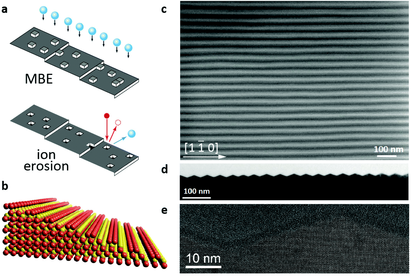 | ||
Fig. 1 Regular nanowire patterns on GaAs(001) produced by low-energy ion irradiation. (a) Schematic illustration of the symmetry between growth by ad-atom deposition in MBE and ion erosion by vacancy creation. Due to the step-edge barrier for ad-atoms (ad-vacancies) nucleation and growth of islands (depression) lead to 3D morphologies. (b) A (115) surface of the GaAs with Ga dimer rows along the [1![[1 with combining macron]](https://www.rsc.org/images/entities/char_0031_0304.gif) 0] direction, which is the direction of the grooves. (c) SEM images of highly-ordered nanogroove patterns formed on GaAs (001) surfaces aligned along the [10] direction after 1 keV Ar+ irradiation at normal incidence for 130 min at 410 °C. (d) and (e) Cross-sectional TEM images of nanogroove pattern on GaAs(001). 0] direction, which is the direction of the grooves. (c) SEM images of highly-ordered nanogroove patterns formed on GaAs (001) surfaces aligned along the [10] direction after 1 keV Ar+ irradiation at normal incidence for 130 min at 410 °C. (d) and (e) Cross-sectional TEM images of nanogroove pattern on GaAs(001). | ||
Ion irradiation, on the other hand, is frequently used to etch materials by sputtering7 and can be easily scaled up to 300 mm wafer size. It can also be employed for nanopatterning surfaces by a self-organized, bottom-up approach.8 The resulting patterns are periodic ripple structures with periodicities down to 15 nm9 and can achieve quite high order as in the case of Si and Ge irradiated with 26 keV Au− ions.10 Such ripple patterns can be applied as templates for growing nanostructured thin films with strong anisotropic magnetic or optical properties.11 Therefore, a broad interest exists for this simple, high-throughput and inexpensive technology for nanopatterning surfaces. The main drawback of this method is that semiconductors are amorphized when ion irradiation is performed at room temperature.12 At elevated temperature, however, ion induced interstitials and vacancies are mobile enough to recombine or to reach the surface before a new ion hits the same region. Thus ion irradiation performed at temperatures higher than the recrystallization temperature prevents amorphization and leads to an additional surface instability due to the ES barrier for surface vacancies.13–20 Accordingly, in analogy to the case under growth conditions, this kind of surface instability leads to the formation of 3D nanostructures (Fig. 1a). Vacancies which are created by the ion impacts during irradiation, nucleate and coarsen to form pits that grow inside the surface.13 The formation of such structures has firstly been observed on metal surfaces, which remain crystalline even at room temperature, due to their high diffusion and non-covalent bonding.14–16
Recently, we have observed regular, dense patterns of inverse pyramids on Ge(001) surfaces irradiated by high fluence 1 keV Ar+ at temperature above 250 °C.21 These patterns exhibit {105} facets and strongly resemble mound patterns grown by MBE if they are reversed. Here, we present the formation of nanogrooves on the (001) surface of group III–V semiconductors (GaAs, InAs) with a zinc-blende structure. Although the symmetry of the surface is four-fold, like the (001) surface of Si and Ge, a symmetry-breaking due to the stacking of alternating planes of Ga (In) and As leads to an almost perfect two-fold symmetry of the resulting patterns even under normal incidence. In combination with enhanced ion-induced surface diffusion this symmetry-breaking driving force leads to faceted periodic nanogroove patterns oriented along the [10] direction with the highest degree of regularity observed so far. Similar ripple patterns have been observed recently by irradiation of GaAs with hyperthermal ion beams (30 eV Ar+), however with much lower regularity.22 Furthermore, on the (111) surfaces of Si and Ge with diamond structure irradiated with high fluence we found peculiar {123} and {356} facets that have not been observed so far. All of these ion induced patterns can be described by a universal generalized continuum equation21,23 by defining a non-equilibrium surface free energy with the required symmetry, giving the formation dynamics with the correct roughening and coarsening behavior.
2. Results
For the erosion process an ion source producing a broad beam of low-energy ions is used to irradiate the surface of single crystalline semiconductors. After ion irradiation with fluences of 1017–1019 cm−2 performed above the recrystallization temperature ordered patterns appear on the surface. Arrays of nanogroove structures with a periodicity of 46 nm are fabricated on GaAs (001) surfaces (Fig. 1c). The orientation of the grooves is always along the [10] direction on GaAs and InAs, i.e. the atomic structure of the facets is similar to Fig. 1b. The degree of order of these nanogroove structures is increasing with the irradiation fluence. Cross-sectional transmission electron microscopy (TEM) images perpendicular to the grooves (Fig. 1d and e) also show clearly the faceting and the high degree of ordering of these structures.
Fig. 2a–f present typical patterns on different semiconductor surfaces after ion irradiation performed at normal incidence above the recrystallization temperature. Faceted nanostructures with different orientations and shapes develop, which are, with respect to the surface, reversed to similar structures found by MBE.24 The periodicity and the shape of the faceted structures can be tuned by the irradiation conditions (temperature and fluence) as well as by using different orientations of the crystalline surfaces, i.e. low-index crystal planes or different miscut angles from these planes. The formation of facets can be also concluded from the corresponding two-dimensional (2D) angle distributions25 (left) and three-dimensional (3D) zoom-in images (right) shown above the AFM images. The symmetry of the patterns reflects the crystal symmetry of the surfaces. For the (001) surface of GaAs (Fig. 2a) and InAs (Fig. 2d) the evolving patterns are periodic, faceted grooves oriented along the [10] direction. This is quite surprising, as the irradiation is performed at normal incidence, thus no asymmetry is imposed by the ion beam. As shown in Fig. 1b, the direction, where dimer rows of Ga (In) are formed due to a (2 × 1) surface reconstruction parallel to the steps,26 is energetically preferred over the formation of As dimer rows. Furthermore, the [10] direction is also the easy diffusion direction of the Ga (In) atoms.27 The 2D angle distribution shows two peaks at ±16° and ±19°, respectively. These polar angles can be identified with the {115} (15.79°) and {114} (19.47°) crystal planes, respectively (Fig. 2g).
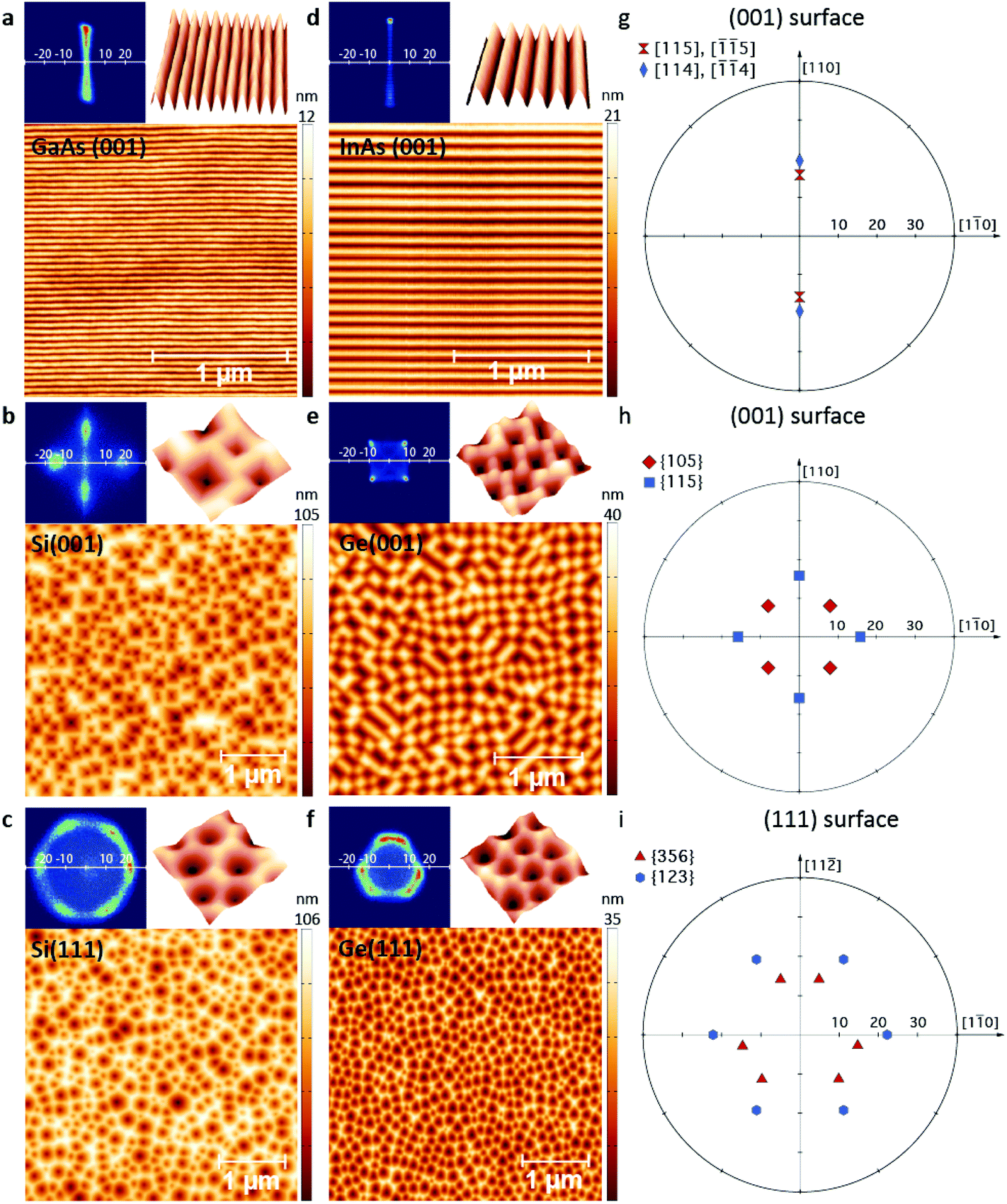 | ||
| Fig. 2 Atomic force microscopy images of nano-patterns fabricated by ion irradiation on the surfaces of different semiconductors. (a) Nanogrooves on GaAs(001), (b) inverse squared pyramids on Si(001), (c) inverse hexagonal pyramids on Si(111), (d) nanogrooves on InAs(001), (e) inverse squared pyramids on Ge(001), and (f) inverse pyramids on Ge(111), respectively. The two-dimensional angle distributions (left) covering an area of ±30° and the three-dimensional AFM images (right) with scanning size of 500 × 500 nm are shown above the AFM images. The horizontal direction of the AFM images is along the [10] direction. (g–i) Polar plots of the geometrical projections of planes of the diamond lattice with respect to the polar (001) surface (GaAs and InAs), to the (001) surface, and to the (111) surface of the diamond lattice (Si, Ge), respectively. The ion irradiation energy and fluence are 1 keV, 1 × 1019 cm−2 Ar+ for (a), (d), (f), 1 keV, 3 × 1018 cm−2 for (e), and 500 eV, 3 × 1018 cm−2 Xe+ for (b) and (c), respectively. The irradiation temperatures are 410 °C for GaAs (a), 320 °C for InAs (d), 530 °C for Si (b, c) and 300 °C for Ge (e, f). | ||
For Si(001) and Ge(001) a 4-fold symmetry can be identified in Fig. 2b and e. For single-element semiconductors the dimer rows in the [10] and [110] directions consist of the same element, i.e. there is no longer a difference in their surface energy, and, consequently, the symmetry breaking disappears. The angle distribution exhibits peaks at 12° for Ge and 16° for Si, which are close to the {105} (11.31°) and {115} (15.79°) planes of the diamond lattice, respectively. The polar plot of the orientation of these facets with respect to the (001) surface is shown in Fig. 2h. The azimuthal orientation of the structures is different for Si(001) and Ge(001). On Si(001) the structures are oriented along the [110] direction, whereas on Ge(001) the structures align along the [100] direction. This is quite peculiar, because Si and Ge have the same crystal structure and exhibit usually the same (2 × 1) surface reconstruction of the (001) surface. The same facets and the rotation of the pattern by 45° between Si and Ge appear in homoepitaxial growth of Si and Ge as well.28–31 The emergence of these edges is attributed to an additional barrier at kink sites, similar to the barrier at step edges. However, the origin of the different orientation of the Si and Ge mound facets has not yet been conclusively clarified.
The patterns on the (111) surface of Si (Fig. 2c) and Ge (Fig. 2f) exhibit a different symmetry. On the Ge(111) surface, inverse pyramidal structures with an isotropic distribution are formed. The corresponding 2D angle distribution reveals a three-fold symmetry in the formation of the facets with a polar angle θ of 13°–16°. Noticeable is the development of a double peak structure in the 2D angle distribution separated by an azimuthal angle of ∼38°. Inspection of the geometrical projection of the possible facets of the diamond lattice with respect to the (111) surface reveals that the measured angle distribution coincides with the {356} facets. As can be seen in the polar plot of the crystal planes in Fig. 2i, six of these facets have the right polar angle of 15°. They appear as three pairs of two poles with a difference in the azimuthal angle of 38.2° and rotated by 120° to each other, in perfect agreement with the experimentally determined facet angles. These facets are typically not observed in homoepitaxial or heteroepitaxial growth of self-assembled Ge nanostructures. Thus, we can conclude that they are ion induced non-equilibrium stable crystal facets.
On the Si(111) surface inverse hexagonal pyramids are formed during ion irradiation. The structure size of these patterns exhibits a much broader distribution than for the patterns on Ge(111). Thus for Si(111) the wavelength selection at the beginning of the pattern formation is much weaker than for Ge(111). Furthermore, the 2D angle distribution shows six peaks with a polar angle of 21°–23° with a hexagonal symmetry. The facets, which correspond to these values are the {123} crystal planes (22.21°) of the diamond lattice, as can be seen in the geometrical projection of the planes with respect to the (111) surface in Fig. 2i.
Due to the fact that the facets are crystal planes, asymmetric facets can also be formed on surfaces with predefined miscut angles. Fig. 3 shows nanogroove patterns on vicinal GaAs(001) surfaces with miscut angles of 6° and 10° in the [110] direction, respectively. The wavelength of the formed nanogrooves increases from 46 nm on GaAs(001) surfaces without miscut (Fig. 1c) to 65 nm (Fig. 3a) and 90 nm (Fig. 3b) for the surface with 6° and 10° miscut angles, respectively. Fig. 3c and d show the cross-sectional TEM of GaAs(001) with a 10° miscut angle. The shape of these nanogrooves becomes asymmetrical with absolute facet angles to the (100) planes of 20° and 21°, respectively. To keep the same angle of the {114} facet with respect to the (001) surface on both sides one sidewall of the groove is elongated, thus increasing the periodicity of the pattern.32 These kinds of structures are particularly interesting to be applied as optical grating devices for ultraviolet light.33
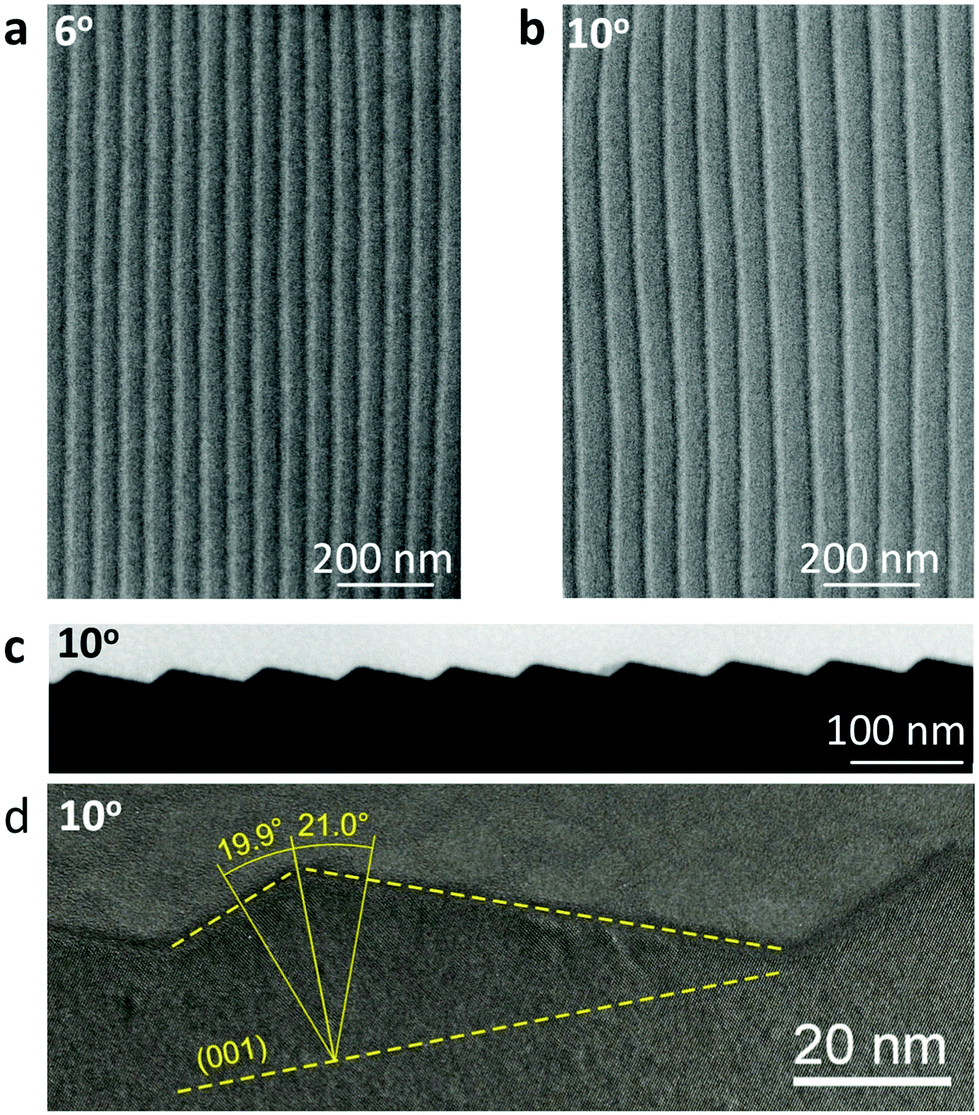 | ||
| Fig. 3 Ordered, asymmetric nanogroove patterns formed on ion irradiated GaAs(001) surfaces with a miscut angle. (a) SEM image of nanogroove structures formed on GaAs(001) with a miscut angle of 6° and (b) with a miscut angle of 10° towards the [110] direction, respectively. (c, d) Cross-sectional TEM images of the nanogroove patterns. The facet angles with respect to the GaAs(001) plane are indicated. | ||
The formation of 3D nanostructures on ion irradiated surfaces at temperatures above the recrystallization temperature can be regarded as the reverse mechanisms to 3D growth in homoepitaxy.16,21,24,34,35 The continuous ion irradiation creates a surface vacancy density, which is much higher than the vacancy density under equilibrium conditions, thus driving additional non-equilibrium surface currents. Due to the step edge barriers, the vacancy diffusion currents are “downhill”, leading to a surface instability.6,23,36 The orientation of the patterns along the crystalline directions and the selection of specific facets on the ion irradiated surfaces indicate that the diffusion currents are dominant and sputtering induced effects, like slope/curvature dependent erosion rates and mass redistribution, can be neglected. Thus the continuum equations, which are typically used to describe the morphology evolution on amorphized surfaces under ion irradiation, do not account for the crystal structure and cannot be used here. On binary materials an additional instability is expected37 due to preferential sputtering of one element changing the stoichiometry of the surface. The coupling of this altered surface layer and the topography can lead to the formation of periodic patterns as well. However, the crystalline GaAs (InAs) are Ga (In) terminated and no preferential sputtering or segregation of one element has been observed.38 Furthermore, even at temperatures below the recrystallization temperature we did not observe any pattern formation on GaAs or InAs, thus on these amorphized surfaces ion induced smoothing dominates at normal incidence.
3. Discussion
In order to describe the formation of patterns with the special symmetries on the different surface orientations we generalized and extended the continuum equation used for the Ge (001) case.21 The evolution of the surface height h(x,t) can be described in a coarse-grain approach by a partial differential equation: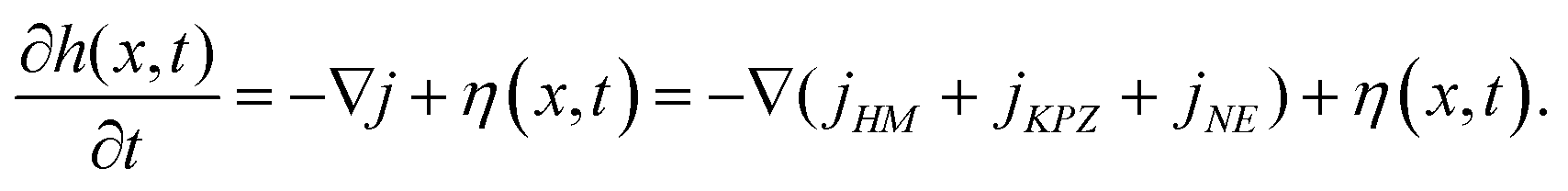 | (1) |
The surface current j includes three contributions: jHM = κ∇(∇2h) is the Herring–Mullins surface diffusion, jKPZ = σ∇(∇h)2 is a nonlinear current (conserved Kardar–Parisi–Zhang term) that breaks the up–down symmetry of the resulting surface, and jNE is the non-equilibrium surface current that includes the instability due to the ES step edge barrier and the formation of facets. Furthermore, a white noise term η(x, t) is included to account for the stochastic nature of the vacancy formation.
Similar to the chemical potential in equilibrium, which determines the vacancy and ad-atom concentrations in thermal equilibrium, a non-equilibrium potential UNE can be defined corresponding to the non-thermal ion induced concentrations of vacancies and ad-atoms. UNE(m) is proportional to the surface density of atoms and is a function of the local slope m = ∇h. The minimization of the non-equilibrium potential with respect to the surface slope induces a non-equilibrium surface current  . Due to the high ion induced density of vacancies and their restricted interlayer transport due to the ES barrier the original surface becomes unstable, i.e. UNE(m) has a local maximum at zero slope m = (0,0). The interplay of this instability and the surface diffusion leads to a wavelength selection at the beginning of ion irradiation. At the minima of UNE(m) the surface current jNE vanishes leading to a selection of the preferred slopes (facets) at later times.
The different surface patterns in Fig. 4 result from appropriate choices of the non-equilibrium potential UNE(m), reflecting the symmetry of the crystalline surface and possessing minima at the respective, experimentally observed facet angles. In Fig. 4 the chosen non-equilibrium potential and results of the numerical integration of the continuum equation with the corresponding 2D angle distributions are presented. The good agreement between the experimentally observed pattern in Fig. 2 and results of the continuum equation in Fig. 4 indicates that the facet formation is strongly linked to surface currents driven by the minimization of the non-equilibrium effective free energy. In analogy to the determination of the chemical potential by observing the shape of crystals grown under equilibrium conditions, we can thus assess the shape and the first minima of the non-equilibrium potential UNE(m) in the vicinity of the original surface exposed to ion irradiation. It is known that under continuous vacancy creation crystal facets can become unstable and non-equilibrium steady state facets of different orientation can be formed.39
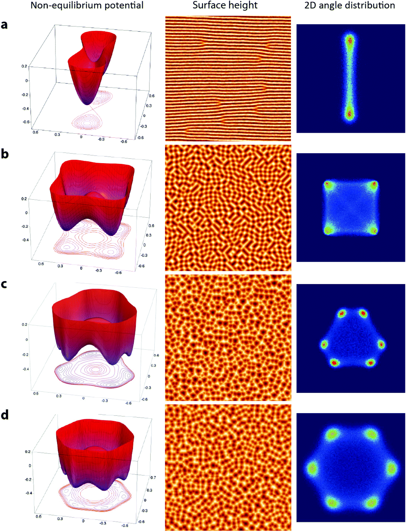 | ||
| Fig. 4 Non-equilibrium potential, surface height, and 2D angle distributions from numerical integrations of the continuum equation for reverse epitaxy. Non-equilibrium potentials have been chosen to have minima at slopes (mx, my) corresponding to the facet angles and symmetries with (a) two-fold (GaAs(001)), (b) four-fold (Ge(001)), (c) three-fold (Ge(111)), and (d) six-fold (Si(111)) symmetry, respectively. | ||
4. Methods
Sample preparation
10 mm × 10 mm samples are cut from epi-ready Si(001), Ge(001), Ge(111), InAs(001) and GaAs(001) wafers. The ion irradiation is performed in a vacuum chamber with a base pressure of 10−8 mbar. The inert gas ions (Ar+ and Xe+) are generated by using a Kaufman-type ion source with a single graphite grid extraction of 50 mm in diameter. During irradiation the chamber is backfilled with Ar or Xe gas at 10−4 mbar through the ion source which is not differentially pumped. The samples are pasted on a Si plate of 15 mm × 15 mm to avoid metal contamination from the sample holder. The samples are heated by a boron nitride heater behind the sample holder. The surface temperature of the irradiating sample is monitored by a pyrometer operated in the wavelength range of 2–2.8 μm, which was pre-calibrated by using a thermocouple. The optimized irradiation conditions for different semiconductor surfaces are listed in Table 1. Two ion fluences of 3 × 1018 cm−2 and 1 × 1019 cm−2 are applied in the irradiation process, which corresponds to the irradiation duration of 38 min and 130 min, respectively. The topography of irradiation induced nanopatterns is characterized by atomic force microscopy (AFM) in tapping and non-contact mode and by scanning electron microscopy (SEM). The crystal quality of the nanostructures is investigated by cross-sectional transmission electron microscopy (TEM).| Materials | Ion species | Ion energy (eV) | Temperature window (°C) |
|---|---|---|---|
| Si(100) | Xe+ | 500 | 480–580 |
| Ge(100) | Ar+ | 1000 | 250–430 |
| Ge(111) | Ar+ | 1000 | 250–380 |
| InAs(100) | Ar+ | 1000 | 180–430 |
| GaAs(100) | Ar+ | 1000 | 200–480 |
Numerical integration
The numerical integration of the continuum equation (1) for reverse epitaxy is performed on a grid of 500 × 500 points with a spacing of Δx = 1 and Δt = 0.01 by a 4th order Runge–Kutta method. The non-equilibrium potentials UNE(m) in Fig. 3 are polynomials up to 8th order in mx and my chosen to have the desired symmetry and minima at slopes corresponding to the observed facets. The non-equilibrium surface currents jNE(m) are calculated analytically from UNE(m) and subsequently used in a Matlab® program to integrate numerically the following continuum equation:
In every integration step white noise with an amplitude of 0.05 has been added. The coefficients used for the numerical integrations for the different cases in Fig. 4 are as follows: (a) ε = 1, κ = 1, σ = −1, (b) ε = 1, κ = 4, σ = −1, (c) ε = 2, κ = 4, σ = −2, and (d) ε = 2, κ = 4, σ = −2. The coefficients for the numerical integration have been chosen solely by the intention to produce patterns with a structure density similar to the AFM images in Fig. 2.
5. Conclusion
In conclusion, we have shown that low-energy ion irradiation of semiconductors above the dynamic recrystallization temperature leads to the spontaneous formation of 3D crystalline structures. To a large extent the here reported erosive pattern formation is analogous to the well-known pattern formation during homoepitaxy and the formation mechanism of these patterns of crystalline structures is universal and can be extended to different crystalline surfaces. These self-assembled structures form on group III–V semiconductors extremely regular patterns of grooves and on elemental semiconductors patterns of inverse pyramids with specific facets. Depending on the crystal surface orientation different symmetries are found: two-fold in the case of GaAs and InAs due to an additional symmetry-breaking mechanism, three-fold for Ge(111), four-fold for Ge(001) and Si(001) surfaces, and six-fold on Si(111). The present technique of self-organized nanogroove formation on group III–V semiconductors may actually be the one yielding the highest degree of regularity available today without pre-patterning. Due to the parallel formation of the nanopatterns by broad ion beam irradiation, which can be scaled up to 300 mm wafer size, this technique is much faster than serial lithography techniques like e-beam or proton writing techniques. We envision that such highly-ordered nanogroove patterns have a great potential for many applications, e.g. as templates for thin film deposition, as catalytic surfaces, and as gratings for UV light.Acknowledgements
The authors acknowledge support from Deutsche Forschungsgemeinschaft (FOR845). X. O. acknowledges the support from One Hundred Talent Program of CAS and PuJiang Talent Program of Shanghai (15PJ1409700). X. W. acknowledges support by the Creative Research Groups of National Science Foundation of China (Grant Nos. 61321492).References
- Y. Huang, X. F. Duan, Q. Q. Wei and C. M. Lieber, Science, 2001, 291, 630–633 CrossRef CAS PubMed.
- E. Dimakis, U. Jahn, M. Ramsteiner, A. Tahraoui, J. Grandal and X. Kong, Nano Lett., 2014, 14, 2604–2609 CrossRef CAS PubMed.
- H. G. Yang, C. H. Sun, S. Z. Qiao, J. Zou, G. Liu, S. C. Smith, H. M. Cheng and G. Q. Lu, Nature, 2008, 453, 638–644 CrossRef CAS PubMed.
- C. Teichert, Phys. Rep., 2002, 365, 335–432 CrossRef CAS.
- J. W. Evans, P. A. Thiel and M. C. Bartelt, Surf. Sci. Rep., 2006, 61, 1–128 CrossRef CAS PubMed.
- J. J. Villain, Phys. I, 1991, 1, 19–42 Search PubMed.
- M. V. R. Murty, Surf. Sci., 2002, 500, 523–544 CrossRef CAS.
- W. L. Chan and E. J. Chason, J. Appl. Phys., 2007, 101, 121301 CrossRef PubMed.
- S. Facsko, T. Dekorsy, C. Koerdt, C. Trappe, H. Kurz, A. Vogt and H. L. Hartnagel, Science, 1999, 285, 1551–1553 CrossRef CAS.
- S. A. Mollick, D. Ghose, P. D. Shipman and R. Mark Bradley, Appl. Phys. Lett., 2014, 104, 043103 CrossRef PubMed.
- J. Fassbender, T. Strache, M. O. Liedke, D. Markó, S. Wintz, K. Lenz, A. Keller, S. Facsko, I. Mönch and J. McCord, J. New J. Phys., 2009, 11, 125002 CrossRef.
- R. Stanley Williams, Solid State Commun., 1982, 41, 153–156 CrossRef.
- T. Michely, K. H. Besocke and G. Comsa, Surf. Sci., 1990, 230, L135–L139 CrossRef CAS.
- C. Teichert, M. Hohage, T. Michely and G. Comsa, Phys. Rev. Lett., 1994, 72, 1682–1685 CrossRef CAS.
- S. Rusponi, C. Boragno and U. Valbusa, Phys. Rev. Lett., 1997, 78, 2795–2798 CrossRef CAS.
- U. Valbusa, C. Boragno and F. B. de Mongeot, J. Phys.: Condens. Matter, 2002, 14, 8153–8175 CrossRef.
- E. Chason, T. M. Mayer, B. K. Kellerman, D. T. Mcilroy and A. J. Howard, Phys. Rev. Lett., 1994, 72, 3040–3043 CrossRef CAS.
- S. J. Chey, J. E. VanNostrand and D. G. Cahill, Phys. Rev. B: Condens. Matter, 1995, 52, 16696–16701 CrossRef CAS.
- L. Li, W. Li, L. Qi, M. Lu, X. Yang and C. Gu, Phys. Rev. B: Condens. Matter, 2005, 71, 155329 CrossRef.
- J. Kim, D. G. Cahill and R. S. Averback, Phys. Rev. B: Condens. Matter, 2003, 67, 045404 CrossRef.
- X. Ou, A. Keller, M. Helm, J. Fassbender and S. Facsko, Phys. Rev. Lett., 2013, 111, 016101 CrossRef.
- D. Chowdhury, D. Ghose, S. A. Mollick, B. Satpati and S. R. Bhattacharyya, Phys. Status Solidi B, 2015, 252, 811–815 CrossRef CAS PubMed.
- D. Moldovan and L. Golubovic, Phys. Rev. E: Stat., Nonlinear, Soft Matter Phys., 2000, 61, 6190–6214 CrossRef CAS.
- G. Apostolopoulos, J. Herfort, L. Daweritz and K. H. Ploog, Phys. Rev. Lett., 2000, 84, 3358–3361 CrossRef CAS.
- The 2 dimensional (2D) angle distribution represents the 2 dimensional Cartesian histogram of the local surface angles calculated from the gradients of the surface in the x- and y-direction respectively:
 .
. - V. P. LaBella, H. Yang, D. W. Bullock, P. M. Thibado, P. Kratzer and M. Scheffler, Phys. Rev. Lett., 1999, 83, 2989–2992 CrossRef CAS.
- K. Shiraishi, Appl. Phys. Lett., 1992, 60, 1363 CrossRef CAS PubMed.
- K. A. Bratland, Y. L. Foo, J. A. N. T. Soares, T. Spila, P. Desjardins and J. E. Greene, Phys. Rev. B: Condens. Matter, 2003, 67, 125322 CrossRef.
- J. Van Nostrand, S. Chey and D. Cahill, Phys. Rev. B: Condens. Matter, 1999, 57, 12536–12543 CrossRef.
- A. Shklyaev and M. Ichikawa, Phys. Rev. B: Condens. Matter, 2001, 65, 045307 CrossRef.
- N. Galianaa, P. Martina, C. Munueraa, M. Varelab, F. Soriaa, C. Ocala, A. Ruiza and M. Alonsoa, Surf. Sci., 2006, 600, 3956–3963 CrossRef PubMed.
- J. N. Aqua, I. Berbezier, L. Favre, T. Frisch and A. Ronda, Phys. Rep., 2013, 522, 59–189 CrossRef CAS PubMed.
- Optical grating effect of nanogroove structure on group III–V surfaces was characterized on PTB (Physikalisch-Technische Bundesanstalt) beamline. The first-order diffraction was clearly observed.
- T. Michely, M. Kalff, G. Comsa, M. Strobel and K. H. Heinig, Phys. Rev. Lett., 2001, 86, 2589–2592 CrossRef CAS.
- G. Costantini, E. B. de Mongeot, C. Boragno and U. Valbusa, Phys. Rev. Lett., 2001, 86, 838–841 CrossRef CAS.
- M. Siegert and M. Plischke, Phys. Rev. Lett., 1994, 73, 1517–1520 CrossRef CAS.
- R. M. Bradley and P. D. Shipman, Phys. Rev. Lett., 2010, 105, 145501 CrossRef.
- Auger Electron Spectroscopy analysis has been done on ion irradiated GaAs (InAs) surfaces at temperature below and above the recrystallization temperature, respectively. In contrast to the low temperature case, where Ga (In) accumulation is seen, no accumulation of Ga (In) is observed at high temperature irradiation.
- P. Bellon, Phys. Rev. Lett., 1998, 81, 4176 CrossRef CAS.

| This journal is © The Royal Society of Chemistry 2015 |