
 Open Access Article
 This Open Access Article is licensed under a
 Creative Commons Attribution 3.0 Unported Licence
Probing resistivity and doping concentration of semiconductors at the nanoscale using scanning microwave microscopy
Enrico
Brinciotti
a,
Georg
Gramse
b,
Soeren
Hommel
c,
Thomas
Schweinboeck
c,
Andreas
Altes
c,
Matthias A.
Fenner
d,
Juergen
Smoliner
e,
Manuel
Kasper
b,
Giorgio
Badino
a,
Silviu-Sorin
Tuca
b and
Ferry
Kienberger
*a
aKeysight Technologies Austria GmbH, Keysight Labs, Gruberstrasse 40, 4020 Linz, Austria. E-mail: ferry_kienberger@keysight.com
bJohannes Kepler University, Biophysics Institute, Gruberstrasse 40, 4020 Linz, Austria
cInfineon Technologies, Failure Analysis, Am Campeon 1-12, 85579 Neubiberg, Germany
dKeysight Technologies Deutschland GmbH, Lyoner Strasse 20, 60528 Frankfurt, Germany
eTechnical University of Vienna, Austria
First published on 11th August 2015
Abstract
We present a new method to extract resistivity and doping concentration of semiconductor materials from Scanning Microwave Microscopy (SMM) S11 reflection measurements. Using a three error parameters de-embedding workflow, the S11 raw data are converted into calibrated capacitance and resistance images where no calibration sample is required. The SMM capacitance and resistance values were measured at 18 GHz and ranged from 0 to 100 aF and from 0 to 1 MΩ, respectively. A tip–sample analytical model that includes tip radius, microwave penetration skin depth, and semiconductor depletion layer width has been applied to extract resistivity and doping concentration from the calibrated SMM resistance. The method has been tested on two doped silicon samples and in both cases the resistivity and doping concentration are in quantitative agreement with the data-sheet values over a range of 10−3 Ω cm to 101 Ω cm, and 1014 atoms per cm3 to 1020 atoms per cm3, respectively. The measured dopant density values, with related uncertainties, are [1.1 ± 0.6] × 1018 atoms per cm3, [2.2 ± 0.4] × 1017 atoms per cm3, [4.5 ± 0.2] × 1016 atoms per cm3, [4.5 ± 1.3] × 1015 atoms per cm3, [4.5 ± 1.7] × 1014 atoms per cm3. The method does not require sample treatment like cleavage and cross-sectioning, and high contact imaging forces are not necessary, thus it is easily applicable to various semiconductor and materials science investigations.
1. Introduction
SMM is a quantitative nanoscale electrical characterization technique operating at broadband microwave frequencies.1–5 It combines the nanoscale spatial resolution of an Atomic Force Microscope (AFM) with the broadband (1–20 GHz) electrical measurement capabilities of the Vector Network Analyser (VNA).6–18 In SMM reflection mode, the VNA sends an incident microwave signal through a conductive platinum tip. Depending on the impedance of the tip/sample interface, part of the microwave signal is reflected and measured by the VNA as scattering S11 reflection signal. Together with the reflection signal coming from the tip/sample interface, reflections are also generated from RF cables and connectors. These add up to the measured S11 signal and a de-embedding step is necessary in order to obtain from the measured S11 calibrated values of relevant physical quantities such as complex impedance, capacitance, and resistance.19–23Recently, a calibration workflow has been introduced to extract in situ (i.e. without the need of a calibration sample) complex impedance values from the measured S11 signal.19 This has been applied to successfully obtain calibrated capacitance and resistance images of semiconductor and dielectric materials.12,19 To obtain intrinsic material properties such as dielectric permittivity and resistivity from the SMM calibrated impedance, typically a tip–sample Finite Element Method (FEM) based model is used.19,24–27 In this process, the calibrated SMM data are compared with the FEM results in order to extract a physical quantity (i.e. permittivity, resistivity, etc.).
In this work we follow another approach: an analytical model is used to extract, from the calibrated SMM resistance image obtained from the S11 measurements, resistivity and doping concentration of a doped silicon substrate. We validated this de-embedding method applying it to two doping profiling samples with known doping and resistivity characteristics.
The technique that we propose offers a valid alternative to Scanning Spreading Resistance Microscopy (SSRM), a well-established technique to perform 1-D and 2-D nanoscale carrier profiling.28–30 In SSRM, the resistance is measured by applying a small bias voltage through a conductive diamond AFM-probe while scanning at a high force across a cleaved cross-sectioned surface. Applying a high tip–sample contact force ensures that the measured resistance is dominated by the spreading resistance rather than by the contact resistance and, for silicon samples, it is also required to penetrate the native oxide and to establish a stable electrical contact.31 The SMM based approach that we propose exploits the capability of microwaves to penetrate through the oxide.12 This implies that there is no need of applying a high contact force. In fact, quantitative SMM imaging can be performed with contact forces in the nN range, three orders of magnitude smaller than the μN contact forces typically used in SSRM. Furthermore, in SMM sample cleavage is not required and, since no high contact forces are required, simple metal tips can be used instead of doped diamond tips.
Our results extend the actual capabilities of the SMM, allowing its use to quantify the resistivity and the dopant density of unknown semiconductor samples directly from the calibrated SMM resistance. The method introduced can have direct applications in materials science and semiconductor industry, particularly in the characterization of thin films and in the failure analysis sectors.
2. Materials and methods
2.1. SMM setup
A commercial transmission line SMM (Keysight Technologies, Santa Rosa, CA, USA) was used in all the experiments. It consists of a standard 5600 Atomic Force Microscope (AFM) interfaced with a 20 GHz Vector Network Analyser (VNA). All measurements were carried out in dry atmosphere (RH < 5%). Rocky Mountain Nanotechnology (RMN) solid platinum AFM tips with 18 N m−1 and 0.3 N m−1 spring constant were used. Fig. 1a shows a sketch of the SMM experimental setup. By using the AFM tip as a nanoscale imaging and microwave probe, SMM allows for simultaneous topographic and electromagnetic (EM) characterization of the sample under test. The ratio of the incident and reflected signal at the AFM tip, the so called scattering S11 parameter, is measured with the VNA. A half-wavelength coaxial resonator in conjunction with a 50 Ω shunt resistor is used to transform the high impedance of the tip–sample to the characteristic 50 Ω impedance of the VNA. The system is designed to obtain a high signal-to-noise ratio (SNR) with good matching conditions every ∼1 GHz, with the exact value depending on the cable lengths. In this work, all the measurements were performed at frequencies between 18–20 GHz, while the SMM works in the range of 1–20 GHz.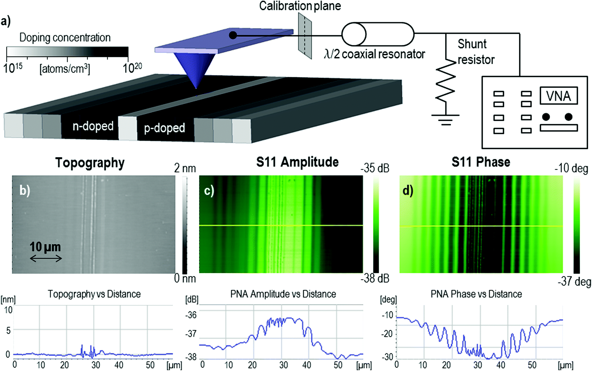 | ||
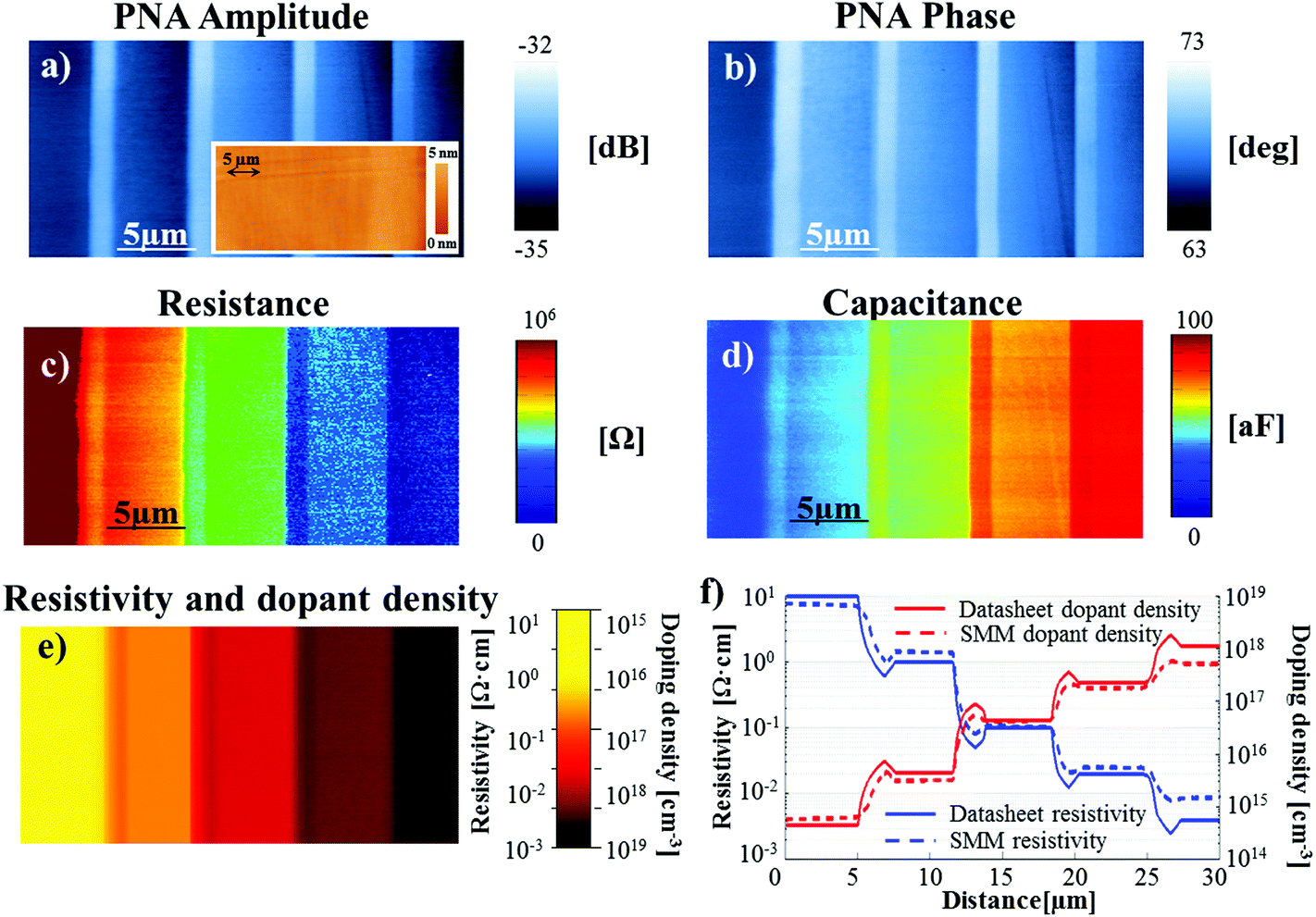
| Fig. 1 (a) Sketch of the SMM experimental setup and of the doped Si sample with flat topography. The sample consists of 10 different n-implant areas (left region) and 10 different p-implant areas (right region), each area with a width of 2 μm, with doping concentrations ranging from 4 × 10¹⁵ to 1 × 10²⁰ atoms per cm3. The SMM raw images of this sample are shown including flat topography (b), S11 amplitude (c) and S11 phase (d). The horizontal cross-sections are given below the images. | ||
2.2. Samples under test
Two commercially available doping samples were used to validate the analytical model. The first sample is a topographically flat doped silicon (Si) sample, produced by Infineon Technologies (Failure Analysis Division, Munich).23 It consists of a p-Si substrate (1015 atoms per cm3) with 10 different p-type and 10 different n-type implant areas, each with 4 × 10¹⁵, 1 × 10¹⁶, 4 × 10¹⁶, 1 × 10¹⁷, 4 × 10¹⁷, 1 × 10¹⁸, 4 × 10¹⁸, 1 × 10¹⁹, 4 × 10¹⁹, and 1 × 10²⁰ atoms per cm3. The doped areas in the active region are 2 μm wide and 200 nm deep. In each doped area the doping level is uniform until 200 nm and then it drops exponentially and completely falls off at roughly 1 μm. The n-doped and p-doped regions are next to each other and therefore can be imaged in one SMM scan. No further processing or cleaning steps were performed prior imaging it with the SMM.The second commercially available doping sample is produced by IMEC CAMS (Center for Advanced Metrology Solutions, Belgium).32,33 It consists of several 5 μm wide layers of silicon with varying donor dopant density ranging between 1 × 10¹⁵ atoms per cm3 and 1 × 10¹⁹ atoms per cm3 grown on a silicon wafer. The wafer is then cleaved to expose the cross sections of the layers. While the Infineon sample can be imaged in a standard top-down configuration, the IMEC sample is imaged in the cross-section profile. Another difference is that the doping depth is 200 nm for the Infineon sample, while in the IMEC sample it extends over the full sample depth (i.e. ∼1 cm).
2.3. Complex impedance calibration
To convert the measured SMM S11 raw data into calibrated complex impedance values, the calibration procedure recently proposed by Gramse et al.19 was used. In this procedure, the complex impedance Z is extracted from the measured S11 using the one-port black-box calibration.20 By simultaneously recording complex S11 and electrostatic force microscopy (EFM) approach curves, the three complex error parameters (e00, e01, and e11) are calculated and used to convert acquired S11 images into admittance images. The three error parameters can be calculated using S11 = e00 + e01S11,a/(1 − e11S11,a), where S11,a = (Zin − Zref)/(Zin + Zref), and Zref is the characteristic impedance of the VNA (i.e. 50 Ω). From the electrostatic force, Fes,2ω, measured at the second harmonic of the excitation voltage v(t) = V0![[thin space (1/6-em)]](https://www.rsc.org/images/entities/char_2009.gif) sin(ωt) in the EFM approach curve, the gradient of the capacitance with respect to the tip-sample distance is obtained by dC/dz = 4Fes,2ω/V02. By integration, the capacitance C(z) can be calculated. Fig. 1a shows the calibration plane located directly before the cantilever chip.
sin(ωt) in the EFM approach curve, the gradient of the capacitance with respect to the tip-sample distance is obtained by dC/dz = 4Fes,2ω/V02. By integration, the capacitance C(z) can be calculated. Fig. 1a shows the calibration plane located directly before the cantilever chip.
2.4. From SMM resistance to resistivity
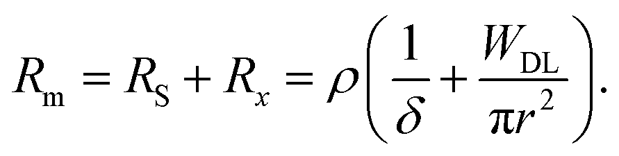
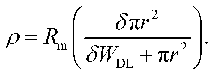
Here we extract the resistivity ρ (Ω m) from the calibrated SMM resistance Rm (Ω). For the incident microwave signal, the surface resistance is defined as RS = ρ/δ,34 where δ (m) is the penetration skin-depth of microwave fields given as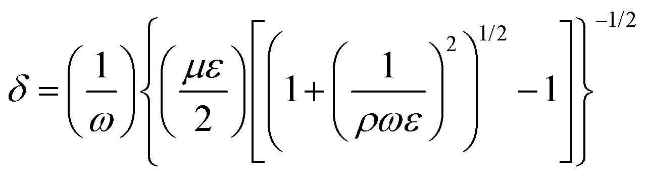 | (1) |
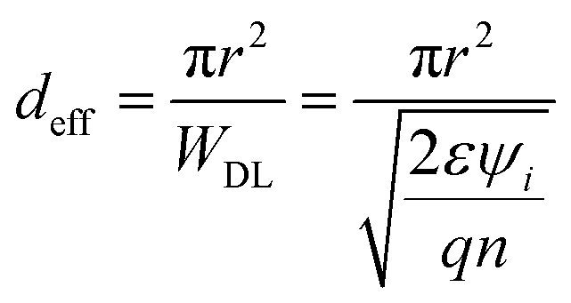 | (2) |
 | (3) |
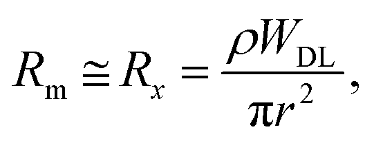
The measured resistance Rm can therefore be modelled as
 | (4) |
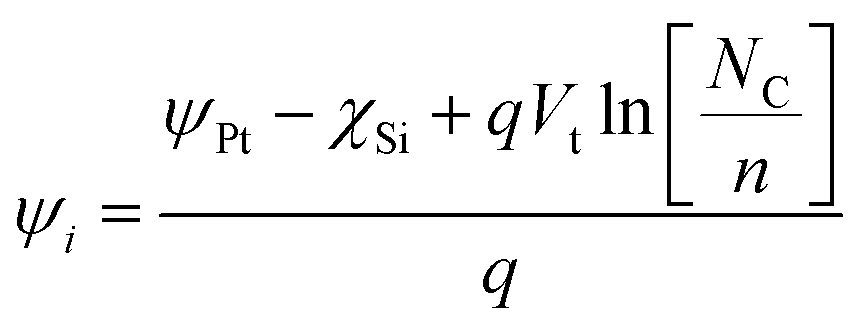
The tip apex radius r can be obtained, as shown elsewhere,37–39 from the experimental EFM capacitance approach curve using the approximation:
| C(r, θ, H, c, cstray, z, h, εr) = Capex + Ccone + Cstray | (5) |
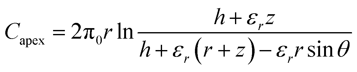
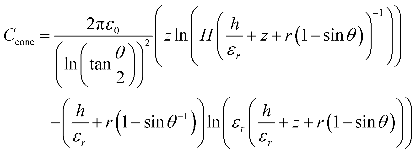
| Cstray = cstrayz + c |
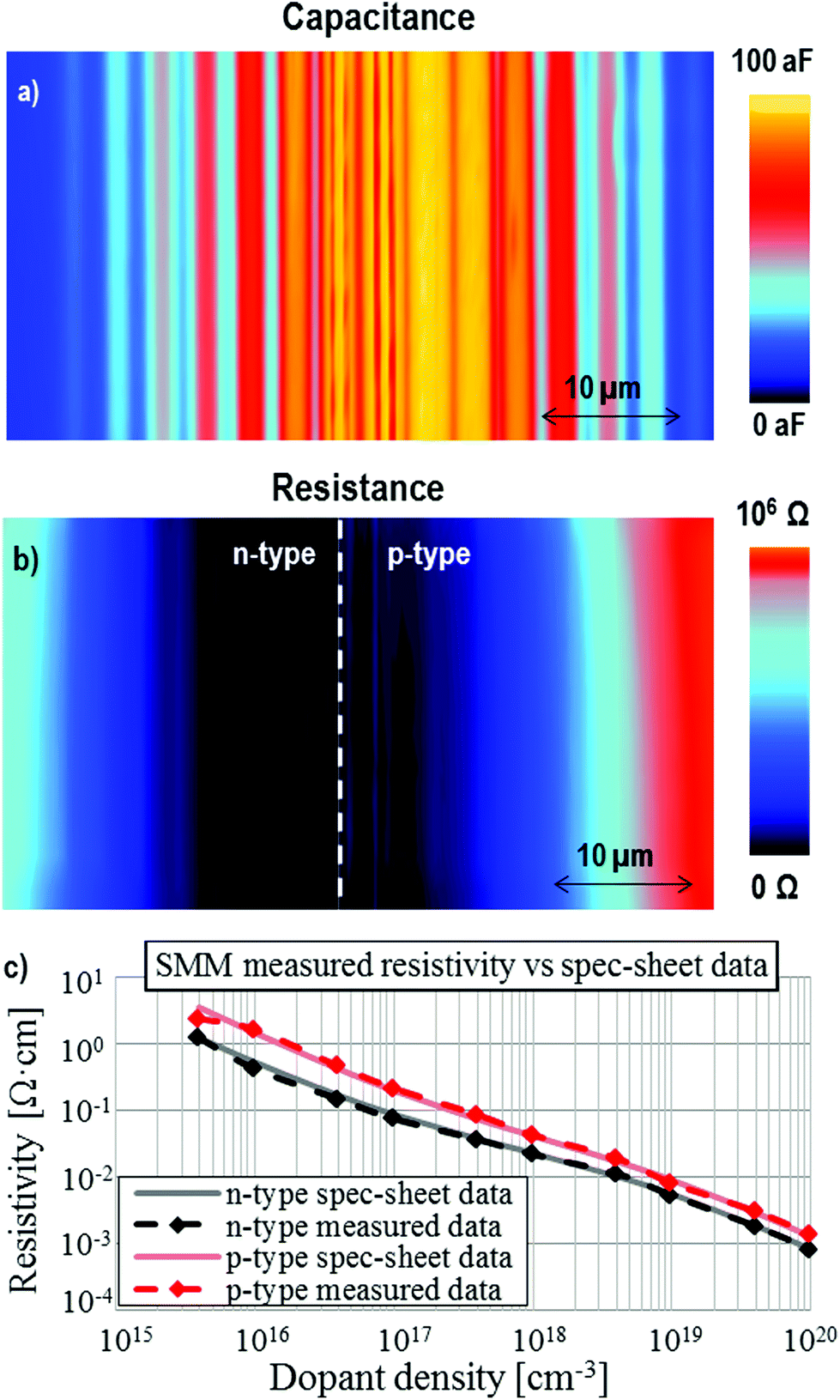 | ||
| Fig. 2 Calibrated SMM data including capacitance (a) and resistance (b) images. Based on the raw S11 amplitude and phase data (see Fig. 1) the three error parameter model was used to calibrate the complex impedance images. The doped Si sample has 10 different n- and 10 different p-implant areas (each 2 μm wide) with doping concentrations ranging from 4 × 10¹⁵ to 1 × 10²⁰ atoms per cm3. The resistivity in (c) is calculated from the calibrated resistance using a tip/sample analytical model including skin depth δ and depletion width WDL. The tip radius r was determined from the EFM dC/dz approach curve. The SMM resistivity is compared to the datasheet resistivity. | ||
Based on eqn (4) the resistivity ρ can be extracted from the measured SMM resistance Rm by
 | (6) |
The resistivity can be converted into doping concentration values by
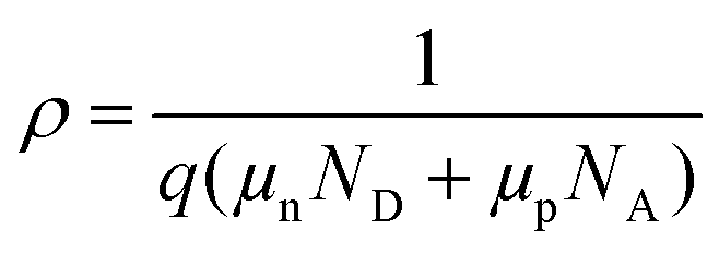 | (7) |
For p-type and n-type silicon, eqn (7) reduces to NA = 1/(qμpρ) and ND = 1/(qμnρ), respectively. It is convenient to express eqn (4) in a form where the dependence of the skin depth δ and of the depletion layer depth WDL on the resistivity ρ is explicit.
Depending on the majority carrier type, the two latter expressions can be substituted with the doping concentration n into eqn (2) and (3).
Therefore WDL, expressed as a function of ρ has the form
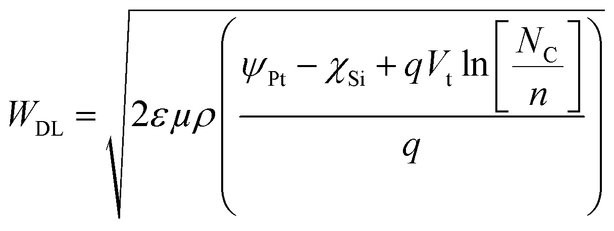 | (8) |
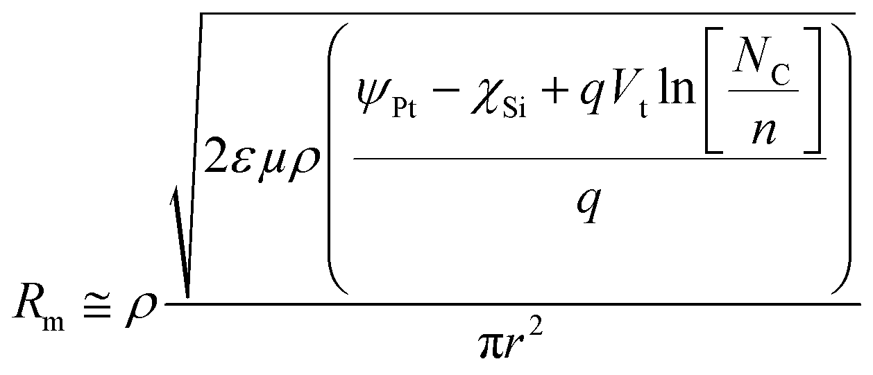
Substituting eqn (1) and (8) in eqn (4), leads to the expression
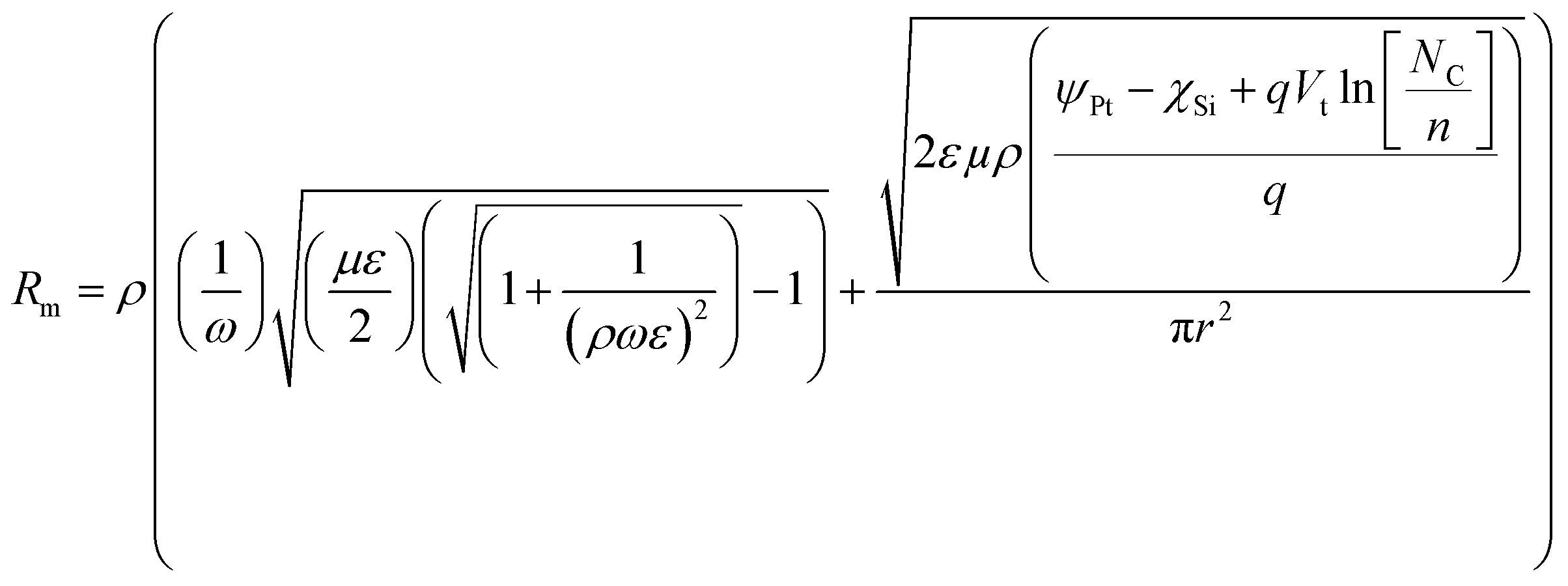 | (9) |
The non-linearity of eqn (9) implies the existence of multiple mathematical solutions where the only one that has a physical meaning, and that corresponds to the unknown resistivity, is the real positive solution. Once the resistivity extracted from the SMM resistance is obtained, the doping concentration can be calculated analytically using eqn (6).
Eqn (9) can be further simplified. For n ≤ 1018 atoms per cm3RS ≪ Rx and eqn (4) reduces to the expression
 | (10) |
3. Results and discussion
The doping samples were imaged with the SMM at 18 GHz and the raw data were acquired including topography, S11 amplitude and S11 phase (Fig. 1). The complex impedance calibration workflow19 was applied resulting in calibrated capacitance and resistance images (Fig. 2a and b). For the impedance calibration, SMM and EFM approach curves were acquired directly on the dopant sample and the three-error parameter model was used to transfer the complex S11 values into tip–sample impedances Z (cf. Materials and methods). There are two main advantages of this complex impedance calibration approach. Firstly, it works in situ on the sample under test and no calibration sample is required. Secondly, the calibration plane is located directly before the cantilever chip, therefore eliminating the contributions from RF cables and connectors. The calibration can be applied to any non-lossy material, like dielectrics or highly conductive materials, for which the change in impedance Z with respect to the tip–sample distance z, Zin(z), is only capacitive. The SMM capacitance measured on the doping sample changes from 0 to 100 aF while the resistance values range between 0 and 1 MΩ (Fig. 2). The resistance image exhibits, as expected, a monotonous trend with lower values in the regions where the dopant concentration is higher. The capacitance image shows higher values in regions where the doping concentration is higher. Also, the individually doped areas can be nicely distinguished.From the SMM resistance Rm (Fig. 2b) we calculated the resistivity (Fig. 2c) according to the following tip–sample resistance model (cf. Materials and methods). A lumped element model34 expresses Rm as two resistors in series, Rm = RS + Rx = ρ(1/δ + WDL/πr2), where RS represents the surface resistance at a given frequency and Rx is the sheet resistance. The AFM tip radius r was determined from an experimental EFM approach curve and the values in this study ranged between 100 nm and 2 μm. δ and WDL are the skin depth and the depletion width, respectively. They both directly depend on the resistivity, electric permittivity ε and the magnetic permeability μ of the sample under test. Therefore, the resistivity ρ can be calculated analytically from the SMM resistance Rm knowing ε and μ of the sample. This procedure can be applied to any Si sample with unknown doping characteristics.
In Fig. 2c the SMM resistivity has been compared to the data-sheet resistivity and for both n-type and p-type regions a quantitative agreement is obtained. For the same doping concentrations, the p-type regions have higher resistivity than the n-type regions. This can be explained considering the higher mobility of the negatively charged impurities in n-type with respect to the positively charged ones in p-type.
In Fig. 3 we show the procedure to obtain SMM resistivity and doping concentration applied on an n-doped Si sample imaged in cross-section geometry. Here, each doped region extends over the entire sample depth (∼1 cm) whereas in the previous sample the implanted regions were only 200 nm–1 μm deep. In both cases the sample surface is flat and the topography shows no information. Therefore, no cross-talk between topography and SMM images is obtained. Applying the same SMM impedance calibration workflow to the raw S11 amplitude and phase images (Fig. 3a and b), calibrated capacitance and resistance images were obtained (Fig. 3c and d). Also in this case the calibrated resistance and capacitance images show lower and higher values for the highly doped areas, respectively. The SMM resistance image was converted into a resistivity and dopant density image using eqn (6) and (7), respectively. Fig. 3e shows the resistivity and dopant density image with the logarithmical colour scale bar where both physical quantities are mapped. Fig. 3f compares the SMM resistivity and doping concentration with the data-sheet values of the sample. Again, a quantitative agreement is obtained for the entire range of doping concentrations. Additionally, the SMM resistivity and doping concentration data clearly shows the intermediate interface layers that separate the individually doped areas.
 | ||
| Fig. 3 SMM raw data (a and b) and calibrated impedance (c and d) of the IMEC n-type Si dopant sample. The sample has a flat topography (inset in a) and different n-doped areas with doping concentrations ranging from 1014 to 1019 atoms per cm3. The 5 μm wide doping areas are separated by 1 μm wide bulk interface layers as observed also in the capacitance and resistance images. The resistivity and doping concentration (e) are calculated from the SMM resistance based on the tip/sample analytical model. (f) Comparison of SMM resistivity and doping concentration values to the datasheet values (provided by IMEC) determined with Secondary Ion Mass Spectroscopy (SIMS). | ||
The depletion width and the skin depth for the standard top-down doping sample are shown in Fig. 4. The depletion width ranges from 4 nm in the most heavily doped region to 574 nm in the region with the lowest doping concentration. The skin depth ranges from 0.7 mm (low doping) to 10 μm (high doping) for the p-type region and from 0.4 mm to 9 μm for the n-type region. Accordingly, the penetration depth is mostly governed by the skin depth, which is frequency dependent. By changing the SMM measurement frequency between 1–20 GHz it is therefore possible to probe different layers in the bulk material. Based on the skin depth dependence on the frequency, we expect on a n-type silicon substrate with doping levels ranging from 4 × 10¹⁵ atoms per cm3 to 1 × 10²⁰ atoms per cm3, the penetration depth to vary between 1.5 mm and 38 μm at 1 GHz, and between 0.3 mm and 9 μm at 20 GHz.
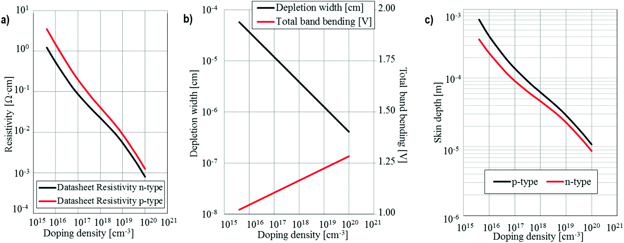 | ||
| Fig. 4 Physical parameters of the doping sample used in the analytical model of the tip/sample resistivity. (a) Datasheet resistivity of the doped Si sample with respect to the different n- and p-implant doping concentrations (Infineon Technologies, Germany). (b) Depletion width [cm; left scale] and total band bending [V; right scale] at different doping concentrations. (c) Skin depth [m] of p-doped and n-doped regions for different doping concentrations. | ||
4. Conclusions
We have demonstrated the ability of SMM to simultaneously probe topography, capacitance, and resistance of semiconductor samples. Additionally, a method is presented to calculate resistivity and doping concentration from SMM resistance that can be applied to any semiconductor sample. The method has been validated on two doping profiling silicon samples, one measured in cross-section and the other one in standard top-down approach. The SMM capacitance and resistance values were characterized at 18 GHz with a noise level of 1 aF for capacitance. Resistance differences as small as 20 Ω could be distinguished. For both samples the SMM resistivity and the doping concentration are in quantitative agreement with the data-sheet values over a range of 10−3 Ω cm up to 101 Ω cm and 1014 atoms per cm3 to 1020 atoms per cm3, respectively.The error associated with the SMM resistivity and dopant density measurements, calculated from the logarithmic difference between SMM and Datasheet in Fig. 3f, is 54% in the region with 1018 atoms per cm3 doping level, 18% in the region with 1017 atoms per cm3 doping level, 5% in the region with 1016 atoms per cm3 doping level, 28% in the region with 1015 atoms per cm3 doping level, and 36.5% in the region with 1014 atoms per cm3 doping level. Accordingly, taking into account the uncertainty, the SMM dopant density in the different doping regions is [1.1 ± 0.6] × 1018 atoms per cm3, [2.2 ± 0.4] × 1017 atoms per cm3, [4.5 ± 0.2] × 1016 atoms per cm3, [4.5 ± 1.3] × 1015 atoms per cm3, [4.5 ± 1.7] × 1014 atoms per cm3.
As opposed to well-established 2-D carrier profiling nanoscale techniques like scanning spreading resistance microscopy (SSRM), the proposed method has the advantage that neither particular sample preparation methods nor high contact imaging forces are required. The lateral resolution of SMM is limited by the probe apex radius while the bulk penetration is mainly determined by the skin-depth. The skin-depth and therefore the microwave penetration depth can be changed by varying the SMM frequency. In this way, frequency dependent depth profiling can be realized. In future, quantitative and calibrated subsurface and tomographic imaging might be possible based on the broadband measurement capabilities of SMM.
Acknowledgements
This work has been supported by the EU-FP7 (NMP-2011-280516, VSMMART-Nano, and PEOPLE-2012-ITN-317116, Nanomicrowave) and Austrian FFG bio-SMM (project number 846532). We would like to thank Prof. Peter Hinterdorfer from JKU Linz for AFM technical assistance.References
- C. P. Vlahacos, et al., Near-field scanning microwave microscope with 100 micrometer resolution, Appl. Phys. Lett., 1996, 69(21), 3272 CrossRef CAS PubMed.
- C. P. Vlahacos, et al., Quantitative topographic imaging using a near-field scanning microwave microscope, Appl. Phys. Lett., 1998, 72(14), 1778–1780 CrossRef CAS PubMed.
- B. J. Feenstra, et al., Near-Field Scanning Microwave Microscopy: measuring local microwave properties and electric field distributions, IEEE MTT-S Int. Microwave Symp. Digest, 1998, 965–968 Search PubMed.
- S. M. Anlage, V. V. Talanov and A. R. Schwartz, Principle of near field microwave microscopy, in Scanning Probe Microscopy: Electrical and Electromechanical Phenomena at the Nanoscale, ed. S. Kalinin and A. Gruverman, Springer-Verlag, New York, 2007, pp. 215–253 Search PubMed.
- M. Tabib-Azar, et al., 0.4 μm spatial resolution with 1 GHz (m = 30 cm) evanescent microwave probe, Rev. Sci. Instrum., 1999, 70(3), 1725–1729 CrossRef CAS PubMed.
- J. Lee, et al., Atomic resolution imaging at 2.5 GHz using near-field microwave microscopy, Appl. Phys. Lett., 2010, 97 CAS.
- K. Ohara and Y. Cho, et al., Non-contact scanning nonlinear dielectric microscopy, Nanotechnology, 2005, 16, S54–S58 CrossRef CAS.
- V. V. Talanov, et al., Noncontact dielectric constant metrology of low-k interconnect films using a near-field scanned microwave probe, Appl. Phys. Lett., 2006, 88, 192906 CrossRef PubMed.
- J. Kim, et al., Near-field scanning microwave microscope using a dielectric resonator, Appl. Phys. Lett., 2003, 83(5), 1032 CrossRef CAS PubMed.
- T. Machida, et al., Development of near-field microwave microscope with the functionality of scanning tunneling spectroscopy, Jpn. J. Appl. Phys., 2010, 49, 116701 CrossRef.
- M. Farina, et al., Disentangling time in a near-field approach to scanning probe microscopy, Nanoscale, 2011, 3(9), 3589–3593 RSC.
- G. Gramse and E. Brinciotti, et al., Quantitative sub-surface and non-contact imaging using scanning microwave microscopy, Nanotechnology, 2015, 26(13), 135701 CrossRef PubMed.
- T. Dargent, et al., An interferometric scanning microwave microscope and calibration method for sub-fF microwave measurements, Rev. Sci. Instrum., 2013, 84, 123705 CrossRef CAS PubMed.
- M. A. Fenner, et al., Quantitative measurement of electric properties on the nanometer scale using atomic force microscopy, in Proc. Int. Semiconductor Conf., Dresden, 2011 Search PubMed.
- C. Plassard, et al., Detection of defects buried in metallic samples by scanning microwave microscopy, Phys. Rev. B: Condens. Matter, 2011, 83(12), 121409 CrossRef.
- A. Tselev, et al., Scanning near-field microwave microscopy of VO2 and chemical vapor deposition graphene, Adv. Funct. Mater., 2013, 23(20), 2635–2645 CrossRef CAS PubMed.
- P. J. Burke, et al., Single-walled carbon nanotubes: Applications in high frequency electronics, Int. J. High Speed Electron. Syst., 2006, 16(4), 977 CrossRef CAS.
- A. Tselev and S. M. Anlage, et al., Broadband dielectric microwave microscopy on micron length scales, Rev. Sci. Instrum., 2007, 78, 044701 CrossRef PubMed.
- G. Gramse, et al., Calibrated complex impedance and permittivity measurements with scanning microwave microscopy, Nanotechnology, 2014, 25(14), 145703 CrossRef CAS PubMed.
- J. Hoffmann, et al., A calibration algorithm for nearfield scanning microwave microscopes, in 12th IEEE Conf. on Nanotechnology, New York, 2012 Search PubMed.
- H. P. Huber, et al., Calibrated nanoscale dopant profiling using a scanning microwave microscope, J. Appl. Phys., 2012, 111 Search PubMed.
- M. Farina, et al., Calibration protocol for broadband near-field microwave microscopy, IEEE Trans. Microwave Theory Tech., 2011, 59, 7–10 CrossRef.
- T. Schweinböck and S. Hommel, Quantitative Scanning Microwave Microscopy: A calibration flow, Microelectronics Reliability, 2014, 54(9–10), 2070 CrossRef PubMed.
- K. Lai, et al., Modeling and characterization of a cantilever-based near-field scanning microwave impedance microscope, Rev. Sci. Instrum., 2008, 79 Search PubMed.
- S. Berweger, et al., Microwave Near-Field Imaging of Two-Dimensional Semiconductors, Nano Lett., 2015, 15(2), 1122–1127 CrossRef CAS PubMed.
- D. E. Steinhauer, et al., Quantitative imaging of dielectric permittivity and tunability with a near-field scanning microwave microscope, Rev. Sci. Instrum., 2000, 71, 2751 CrossRef CAS PubMed.
- J. H. Lee, et al., Quantitative analysis of scanning microwave microscopy on dielectric thin film by finite element calculation, Rev. Sci. Instrum., 2001, 72, 1425 CrossRef CAS PubMed.
- S. Wu and T. Hopson, “SMM Imaging of Dopant Structures of Semiconductor Devices”, Agilent Application Note, January 2014, 5991-0562EN.
- P. Eyben, et al., Scanning spreading resistance microscopy (SSRM) 2d carrier profiling for ultra-shallow junction characterization in deep-submicron technologies, Mater. Sci. Eng. B, 2005, 124–125, 45 CrossRef PubMed.
- P. Eyben, et al., Scanning spreading resistance microscopy and spectroscopy for routine and quantitative two-dimensional carrier profiling, J. Vac. Sci. Technol., B: Microelectron. Nanometer Struct., 2002, 20, 471 CrossRef CAS.
- P. De Wolf, et al., Status and review of two-dimensional carrier and dopant profiling using scanning probe microscopy, J. Vac. Sci. Technol., B, 2000, B 18, 361 Search PubMed.
- T. Trenkler, et al., Two-dimensional profiling in silicon using conventional and electrochemical selective etching, J. Vac. Sci. Technol., B: Microelectron. Nanometer Struct., 1998, 16, 349 CrossRef CAS.
- T. Clarysse, et al., Epitaxial staircase for the calibration of electrical characterization techniques, J. Vac. Sci. Technol., B: Microelectron. Nanometer Struct., 1998, 16, 394 CrossRef CAS.
- A. Imtiaz, et al., Frequency-selective contrast on variably doped p-type silicon with a scanning microwave microscope, J. Appl. Phys., 2012, 111, 093727 CrossRef PubMed.
- S. M. Sze and K. Ng Kwok, Physics of Semiconductor devices, John Wiley and Sons, Inc., Hoboken, New Jersey, 2007 Search PubMed.
- H. Bentarzi, Transport in Metal-Oxide-Semiconductor Structures, Springer-Verlag, Berlin Heidelberg, 2011 Search PubMed.
- G. Gomila, et al., Finite-size effects and analytical modeling of electrostatic force microscopy applied to dielectric films, Nanotechnology, 2014, 25 Search PubMed.
- G. Gomila, et al., Nanoscale capacitance microscopy of thin dielectric films, J. Appl. Phys., 2008, 104 Search PubMed.
- L. Fumagalli, et al., Dielectric-constant measurement of thin insulating films at low frequency by nanoscale capacitance microscopy, Appl. Phys. Lett., 2007, 91 Search PubMed.
| This journal is © The Royal Society of Chemistry 2015 |