
 Open Access Article
 This Open Access Article is licensed under a
 Creative Commons Attribution 3.0 Unported Licence
Fully understanding the positive roles of plasmonic nanoparticles in ameliorating the efficiency of organic solar cells†
Dan
Chi‡
a,
Shudi
Lu‡
a,
Rui
Xu
b,
Kong
Liu
a,
Dawei
Cao
b,
Liaoyong
Wen
b,
Yan
Mi
b,
Zhijie
Wang
*a,
Yong
Lei
 *b,
Shengchun
Qu
*a and
Zhanguo
Wang
a
*b,
Shengchun
Qu
*a and
Zhanguo
Wang
a
aKey Laboratory of Semiconductor Materials Science, Institute of Semiconductors, Chinese Academy of Sciences, Beijing, 100083, People's Republic of China. E-mail: wangzj@semi.ac.cn; qsc@semi.ac.cn
bInstitut für Physik & IMN MacroNano@ (ZIK), Technische Universität Ilmenau, 98693 Ilmenau, Germany. E-mail: yong.lei@tu-ilmenau.de
First published on 19th August 2015
Abstract
Herein, we constructed inverted PBDTTT-CF:PC70BM bulk-heterojunction organic solar cells by introducing Au nanoparticles to a ZnO buffer layer and a great improvement in energy conversion efficiency has been realized. To discover the positive roles of such plasmonic nanoparticles in the process of solar energy conversion, photovoltaic devices with the same architecture but different sized Au nanoparticles were purposely fabricated and it has been observed that the overall efficiency can be remarkably improved from 6.67% to 7.86% by embedding 41 nm Au nanoparticles in the buffer layer. The devices with other sizes of Au nanoparticles show a relatively low performance. Subsequent investigations including finite difference time domain simulation and transient photoluminescence studies reveal that the existence of the plasmonic particles could not only improve the optical absorption and facilitate the exciton separation, but can also benefit the collection of charge carriers. Thus, this paper provides a comprehensive perspective on the roles of plasmonic particles in organic solar cells and insights into the photo energy conversion process in the plasmonic surroundings.
Introduction
Recently, organic solar cells (OSCs) have attracted extensive attention owing to their great advantages including low-cost accessibility, easy scalability and mechanical flexibility,1–6 and a high power conversion efficiency (PCE) over 7% has been realized.7–10 Though various efforts have been focused on designing low-bandgap polymers as well as developing and optimizing new device architectures,11–15 the performance of OSCs is still limited by the inadequate light absorption resulting from the thin active layer, which has to be utilized due to the low carrier mobility and short exciton diffusion length in organic materials.16–18In order to improve the light harvesting properties of the OSC device, plasmonic metallic nanoparticles (NPs) have been incorporated in the active layer or buffer layer.19–21 The well-known localized surface plasmon resonance (LSPR) and anti-reflection effects induced by the metallic NPs could help to ameliorate light absorption greatly.22,23 More importantly, the LSPR of metallic NPs like gold (Au), silver (Ag), platinum (Pt) and palladium (Pd) can be spectrally tuned by changing the corresponding sizes, shapes and dielectric environments,24–26 thereby offering a good platform for optimizing the light absorption efficiency of OSC devices without sacrificing the exciton and charge transport efficiencies.22,23,27 However, the roles of these metallic NPs in OSC devices shall not be limited to improving light harvest, and the relevant functionality nature also needs to be investigated extensively.
In this paper, we optimize the performance of inverted OSCs, ITO/Au NPs:ZnO/PBDTTT-CF:PC70BM/MoO3/Ag, by manipulating the LSPR properties of the metallic NPs. We observe that the PCE has been dramatically improved from 6.67% to 7.86% by introducing 41 nm sized Au NPs to the ZnO buffer layer. Further experimental and theoretical investigations reveal that the plasmonic NPs improve the overall efficiency through three aspects: enhancing light absorption of the system via LSPR and anti-reflection effects; amplifying the generation rate and dissociation efficiency of the excitons; reducing the resistance of the system due to the conductive nature of metallic particles. Thus this work provides deep insights into the photo energy conversion process in the OSCs employing plasmonic metallic particles.
Results and discussion
The Au NPs used herein were synthesized by a standard approach using sodium citrate (C6H5Na3O7·2H2O) to reduce chloroauric acid (HAuCl4) and the size was controlled by the amount of sodium citrate. Fig. 1 shows transmission electron microscopy (TEM) images of the resulting NPs prepared in various amounts of sodium citrate, where the average size of each resultant could be gauged as 16 nm, 25 nm, 41 nm and 72 nm, respectively. Such differentiation in geometrical parameters generates a great specificity in the plasmonic properties of each specimen, thereby offering a good chance to introduce these plasmonic NPs to the architecture of photovoltaic devices to optimize the corresponding energy conversion efficiency.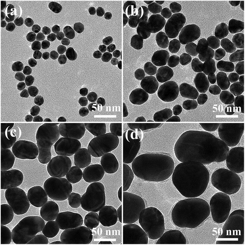 | ||
| Fig. 1 TEM images of Au NPs with different diameters. | ||
Fig. 2a shows the absorbance spectra of the as-prepared Au NPs. The measurement was performed in the aqueous solution. In order to make a better comparison, we normalized each spectrum at the highest peak position. As revealed by these spectra, with the increase of the particle size, the main plasmonic absorption peak shifts to the red direction and the width of the resulting peak broadens. These observations are well consistent with the reported phenomena.24,28,29 To optimize the performance of the OSCs herein, we utilize these particles as the functional material in the ZnO buffer layer. The distribution of the Au NPs is sparse, since the concentration of the particle solution for preparing the Au NP/ZnO film is controlled to as low as 0.01 wt%. Such a distribution could reduce the inefficient light blocking by Au NPs, due to the fact that the incident light is from the ITO direction. Fig. 2b presents the finite difference time domain (FDTD) simulated electric field intensity distribution around the NPs under 700 nm illumination. The simulation was carried out by strictly following the real dielectric surroundings of the plasmonic particles, on ITO glass and in the ZnO film. All these samples have the highest electric field around the surface of the particles and the field decays to the ZnO film. In addition, the symmetric profile of the electric field distribution indicates a dipolar mode of the plasmonic absorption nature. By comparing the electric field intensities of these different particles, we could clearly discover that the field intensity presents a decaying trend with the increase of the particle size, indicative of a deteriorated absorbance intensity for the devices with large Au NPs. Fig. 2c portrays the absorbance spectra of the structure of ITO/Au NPs:ZnO/PBDTTT-CF:PC70BM with various Au particle sizes. The profiles of these spectra show great similarity to that of the sample without Au NPs and the peak of the Au in the range of 500–600 nm is hard to identify, due to the overlapping between the absorbance spectra of the plasmonic particles and the active polymer layer, and to the ignorable absorbance intensity of the Au NP film in comparison with that of the active layer, as shown in Fig. S1.† However, the samples with Au NPs show a great improvement in comparison with the bare sample, suggesting that the presence of the plasmonic particles contributes remarkably to absorption of the structure. Moreover, with the increase of the NP size, the absorbance intensity decreases, in good agreement with the analysis on the electric field distribution.
 | ||
| Fig. 2 (a) Absorbance spectra of Au NPs with different diameters. (b) The FDTD simulated electric field intensity distribution around the nanoparticles under 700 nm illumination. (c) Absorbance spectra of the structure of ITO/Au NPs:ZnO/PBDTTT-CF:PC70BM with various Au particle sizes. | ||
Fig. 3a depicts the schematic structure of the devices with Au NPs. The incident light is from the ITO direction. The Au NP:ZnO buffer layer is employed as the electron collection layer and the MoO3/Ag layer is for harvesting the holes generated in the active layer. As revealed in Fig. 3b, the thicknesses of the Au NPs:ZnO and active organic layers could be estimated as 35 nm and 105 nm, respectively. The current density–voltage (J–V) curves of the relevant devices are shown in Fig. 3c and the corresponding performance parameters are summarized in Table 1, in addition to the ideality factor n and the reverse saturation current density J0, which have been extracted from dark J–V curves.30,31 These curves and parameters reveal that all the devices with Au NPs perform better than the bare device and the solar cell containing 41 nm Au NPs presents the best performance. By adding the 41 nm Au NPs to the buffer layer, the open circuit voltage (VOC), short circuit current density (JSC), fill factor (FF) and PCE can be prominently amplified from 0.746 V to 0.751 V, from 14.49 mA cm−2 to 15.81 mA cm−2, from 61.7% to 66.2% and from 6.67% to 7.86%, respectively. The corresponding external quantum efficiency (EQE) spectra of these two devices are presented in Fig. 3d. In the whole scanned wavelength range, the device with 41 nm Au NPs always possesses a higher EQE than the bare sample, which is consistent with the information shown in Table 1 and Fig. 3c. Herein all the conditions for device fabrication have been optimized and the details in optimizing the ZnO thicknesses, Au density distribution and the position of Au NPs are given in the ESI (Fig. S2–S4†).
 | ||
| Fig. 3 (a) The schematic of the device structure. (b) The cross-sectional scanning electron microscopy image of the device with the structure of glass/ITO/Au NPs:ZnO/PBDTTT-CF:PC70BM/MoO3/Ag. (c) J–V curves of the devices with various Au particle sizes. (d) EQE spectra of the device without Au NPs and the device with 41 nm Au NPs. | ||
| The diameter of Au NPs (nm) | V OC (V) | J SC (mA cm−2) | FF (%) | PCE (%) | R s (Ω cm2) | R sh (kΩ cm2) | n | J 0 (mA cm−2) |
|---|---|---|---|---|---|---|---|---|
| 0 | 0.746 ± 0.0049 | 14.49 ± 0.2903 | 61.7 ± 0.2927 | 6.67 ± 0.1531 | 6.01 ± 0.2847 | 0.55 ± 0.1692 | 1.68 ± 0.0286 | 2.50 × 10⁻⁷ ± 5.33 × 10⁻⁸ |
| 16 | 0.747 ± 0.0015 | 14.96 ± 0.2949 | 62.6 ± 0.4445 | 6.99 ± 0.1781 | 5.37 ± 0.2429 | 0.54 ± 0.1501 | 1.64 ± 0.0152 | 1.65 × 10⁻⁷ ± 2.19 × 10⁻⁸ |
| 25 | 0.753 ± 0.0059 | 15.21 ± 0.2687 | 63.8 ± 0.3763 | 7.31 ± 0.0986 | 5.23 ± 0.2598 | 0.54 ± 0.1076 | 1.59 ± 0.0167 | 7.90 × 10⁻⁸ ± 2.60 × 10⁻⁸ |
| 41 | 0.751 ± 0.0027 | 15.81 ± 0.3157 | 66.2 ± 0.4581 | 7.86 ± 0.1928 | 4.51 ± 0.2805 | 0.65 ± 0.1941 | 1.51 ± 0.0207 | 4.15 × 10⁻⁸ ± 2.55 × 10⁻⁸ |
| 72 | 0.750 ± 0.0049 | 15.00 ± 0.2259 | 62.0 ± 0.3784 | 6.98 ± 0.1332 | 5.87 ± 0.2221 | 0.51 ± 0.1791 | 1.66 ± 0.0148 | 2.17 × 10⁻⁷ ± 1.87 × 10⁻⁸ |
Such a performance improvement could be attributed to the specific properties of the plasmonic NPs. As demonstrated in Fig. 3c and Table 1, when the size of the Au particles increases from 16 nm to 41 nm, the PCE is obviously ameliorated. As the size reaches 72 nm, the PCE drops. However, the FDTD simulation and absorbance spectra of the structure reveal that the increasing size of the plasmonic particles from 16 nm to 72 nm weakens the absorption capability of the devices, though all the devices with Au particles have a higher absorbance than the bare device. These results point out that the absorption improvement induced by the plasmonic particles should not be the only reason for the performance improvement.
In order to investigate the effect of Au NPs on the exciton generation and dissociation of the devices, the maximum exciton generation rate (Gmax) and the exciton dissociation probability (P[E,T]) are particularly explored, using the method previously reported.32–34 The dependence of the photocurrent density (Jph) on the effective voltage (Veff) is displayed in Fig. 4a. Herein, Jph is given by Jph = JL − JD, where JL and JD are the current densities under illumination and in the dark, respectively. Veff is described by Veff = V0 − Va, where V0 is the voltage when Jph = 0 and Va is the applied voltage. As illustrated in Fig. 4a, Jph increases linearly with the effective voltage and then saturates at high effective voltage. The value of the saturation photocurrent density Jsat, which is independent of the bias and temperature, can be derived from Fig. 4a directly. Given that all of the photogenerated excitons are dissociated and contribute to the current at high Veff, Gmax can be calculated by Jsat = qGmaxL, where q is the electronic charge and L is the thickness of the active layer. The resulting Gmax values for the reference device and the device with 41 nm Au NPs are 9.00 × 1027 m−3 s−1 (Jsat = 14.54 mA cm−2) and 10.43 × 1027 m−3 s−1 (Jsat = 16.85 mA cm−2), respectively. The impressive enhancement (about 15.9%) in Gmax suggests that the presence of the plasmonic particles amplifies the exciton generation rate. The inset in Fig. 4a shows the Gmax dependence on the particle size. With the increase of particle size from 16 nm to 41 nm, Gmax shows an increasing tendency. As the size reaches 72 nm, Gmax decreases. However, the absorbance spectra and the FDTD simulation have indicated that the increasing size of the particles weakens the absorption capability of the devices. Such a mismatch points to the fact that the device with smaller NPs possesses a higher inefficient utilization of solar energy and the photons absorbed by the smaller plasmonic particles cannot be converted into free carriers efficiently, though the absorption ability of the relevant device is higher. The exciton dissociation probability can be expressed as Jph = qGmaxP[E,T]L. The corresponding values of P[E,T] at any Veff could be attained from the plot of the normalized photocurrent density Jph/Jsat, which is displayed in Fig. 4b. The curves of P[E,T] vs. Veff and P[E,T] vs. particle size as shown in Fig. 4b present the same trend with those in the analyses on Gmax, therefore implying that the exciton dissociation possibility could also be impacted by the plasmonic particle size.
 | ||
| Fig. 4 (a) Jph–Veff curves of the devices with and without Au NPs, respectively. The inset shows the dependence of the Gmax on the diameters of Au NPs. (b) P[E,T]–Veff curves of the devices with and without Au NPs, respectively. The inset shows the dependence of the P[E,T] on the diameters of Au NPs. (c) Transient PL decays of the structures of ITO/Au NPs:ZnO/PBDTTT-CF:PC70BM with different sizes of Au NPs. The inset gives the dependence of the lifetime on the diameters of Au NPs. (d) Impedance spectra of the corresponding devices. | ||
To support the analysis on exciton dissociation experimentally, we performed transient photoluminescence (PL) measurements for these devices. As shown in Fig. 4c, in comparison with the sample without Au particles, the samples with the plasmonic particles present a faster decay, demonstrating that the plasmonic NPs promote the separation of the photogenerated excitons. For analyzing these results in a more detailed manner, we fit these decay curves using a bi-exponential model and the resulting lifetime as a function of particle size is displayed as the inset in Fig. 4c. It is to be noted that the tendency of the transient PL lifetime vs. particle size matches well the trend in the analysis of P[E,T]. The fitting parameters are given in the ESI (Table S1†). Fig. 4d presents the impedance spectra of the devices used herein and the spectra demonstrate that the resistance of the device exhibits a decreasing feature with the increase of the size of the plasmonic particles, given that the semicircle in a Nyquist plot at high frequencies is characteristic of the charge transfer process and the diameter of the semicircle is estimated to be equal to the charge transfer resistance.35,36 The resistance decrease indicates that the presence of Au NPs helps in improving the charge transfer of the system. Sun et al. reported that for the ITO/TiOx–Au–TiOx/perovskite based solar cells, the plasmon-induced charge injection across the Schottky barrier fills the trap states in TiOx and results in improved conductivity.37 In our system, the improved conductivity in the presence of Au NPs could be due to a similar reason.
One issue that we should pay attention is the performance deterioration of the device with 72 nm Au particles. The thickness of the ZnO buffer layer is around 35 nm, as gauged by the scanning electron microscopy (SEM) images in Fig. 3b. When the 72 nm Au particles are buried in this layer, the resulting surface should be quite rough, which could make the subsequent active polymer layer rough accordingly. As shown in Fig. 5(a–e), the enlarging size of the Au NPs worsens the smoothness of the Au NP:ZnO film and the film with 72 nm Au NPs presents the highest roughness. Fig. 5(f–j) give the atomic force microscopy (AFM) images of these films after spin-coating the active layer. As we expected, the architecture with 72 nm Au NPs exhibits the highest roughness of the polymer layer among these samples. Such a deterioration in the polymer morphology should be responsible for the lower performance of the relevant device. On the other hand, it is unavoidable to expose the large sized Au particle to the active layer. The exposed parts of Au NPs in the polymer could also behave as the recombination centers for charge carriers, thereby weakening the performance further.
 | ||
| Fig. 5 (a–e) The AFM morphology images of ZnO films with various Au NPs: (a) 0 nm, (b) 16 nm, (c) 25 nm, (d) 41 nm, (e) 72 nm. (f–j) AFM images of PBDTTT-CF:PC70BM layers with different Au NPs:ZnO underneath: (f) 0 nm, (g) 16 nm, (h) 25 nm, (i) 41 nm, (j) 72 nm, the root-mean-square roughness is 0.648 nm, 0.702 nm, 0.871 nm, 0.909 nm and 1.01 nm for each sample, respectively. | ||
To check the feasibility of the strategy in designing the buffer layer using plasmonic particles to other categories of OSCs, we fabricated the conventional structured solar cells based on P3HT:PC60BM. The results shown in Fig. S5† exhibit the same trend as that of the solar cells on the basis of PBDTTT-CF:PC70BM. The best PCE has been realized as 4.07% for the sample with 41 nm Au NPs, while the device without Au NPs only has a PCE of 3.29%.
Overall, we clarify that the dramatic power conversion efficiency improvement of organic solar cells by introducing plasmonic nanoparticles to the buffer layer is not only owing to the absorption enhancement by the scattering and localized surface plasmon resonance effects. The investigations, both from the experimental aspect to the simulation aspect and from the solid state view to the ultra-fast transient state view, reveal that the metallic nanoparticles could also be of great benefit for improving the generation rate and dissociation efficiency of the excitons as well as for reducing the resistance of the device. In addition, without using any complicated procedures to modify the polymers and molecules, the optimized energy conversion efficiency in our system is realized as 7.86%, which is almost the highest for the polymer solar cells based on PBDTTT-CF:PC70BM.38,39
Conclusion
In summary, the roles of the plasmonic NPs in promoting the PCE of the OSCs have been realized in the following aspects: enhancing the absorption of the structure by scattering and LSPR effects; increasing the exciton generation rate; promoting the exciton separation; and reducing the resistance of the system. Therefore, a remarkable PCE as high as 7.86% has been attained. This paper provides a comprehensive understanding of the roles of the plasmonic particles and a good strategy for the configuration of solar cells based on metallic NPs.Experimental
Device fabrication
All devices were fabricated using the following procedures. Firstly, the indium tin oxide (ITO) patterned glass substrates were cleaned by using a detergent and sonicated in deionized water, acetone, and isopropanol for 10 min, respectively. Then, the ITO substrates were dried with nitrogen and exposed to O2 plasma for 6 min prior to spin-coating the ZnO thin films at 3000 rpm for 40 s. The precursor solution for fabricating ZnO thin films was prepared by dissolving zinc acetate dihydrate and 2-ethanolamine with a molar ratio of 1![[thin space (1/6-em)]](https://www.rsc.org/images/entities/char_2009.gif) :1 into methoxyethanol.40,41 The precursor solution with the concentration of 1 M was the optimal amount recipe. For fabrication of the devices with plasmonic particles, the pre-prepared aqueous solution containing 0.01 wt% Au particles was spin-coated on the ITO glass prior to depositing the ZnO film. The Au NPs were prepared with HAuCl4 and C6H5Na3O7·2H2O as reported previously.42,43 The ZnO-coated substrates were then annealed at 200 °C for 10 min in air and placed into a nitrogen-filled glove box. The crystalline quality analysis of the ZnO film is given in the ESI (Fig. S6†).
:1 into methoxyethanol.40,41 The precursor solution with the concentration of 1 M was the optimal amount recipe. For fabrication of the devices with plasmonic particles, the pre-prepared aqueous solution containing 0.01 wt% Au particles was spin-coated on the ITO glass prior to depositing the ZnO film. The Au NPs were prepared with HAuCl4 and C6H5Na3O7·2H2O as reported previously.42,43 The ZnO-coated substrates were then annealed at 200 °C for 10 min in air and placed into a nitrogen-filled glove box. The crystalline quality analysis of the ZnO film is given in the ESI (Fig. S6†).
For the PBDTTT-CF (poly[1-(6-{4,8-bis[(2-ethylhexyl)oxy]-6-methylbenzo[1,2-b:4,5-b′]dithiophen-2-yl}-3-fluoro-4-methylthieno[3,4-b]thiophen-2-yl)-1-octanone]):PC70BM ([6,6]-phenyl-C70-butyric acid methyl ester) OSCs, the active layer was formed by spin-coating PBDTTT-CF:PC70BM at 800 rpm for 90 s in an o-dichlorobenzene (ODCB) solution containing 3 vol% 1,8-diiodooctane, 10 mg ml−1 PBDTTT-CF and 15 mg ml−1 PC70BM. Finally, 2 nm MoO3 and 80 nm Ag electrodes were deposited at a base pressure of 5.0 × 10⁻⁵ Pa. For the P3HT (poly(3-hexylthiophene)):PC60BM ([6,6]-phenyl-C60-butyric acid methyl ester) OSCs, Au NPs were firstly spin-coated on the ITO substrates, followed by spin-coating poly(3,4-ethylenedioxythiophene):poly (styrenesulfonate) (PEDOT:PSS, Baytron PVP A1 4083) and a 10 min thermal annealing at 140 °C. Then, the active blend layer was formed by spin-coating (with 15 mg ml−1 P3HT and 12 mg ml−1 PC60BM in ODCB solution at 500 rpm for 18 s followed by solvent annealing at room temperature for 40 min), and was thermally annealed at 110 °C for 10 min. After that the top electrode consisting of 25 nm calcium (Ca) and 80 nm aluminum (Al) was thermally deposited. The active area of the device was optically measured as 4.4 mm2.
Measurements
A Keithley 2400 was used to measure the J–V characteristics of the devices under AM 1.5 illumination with an intensity of 100 mW cm−2 (450 W Newport 6279 NS solar simulator). The surface morphology of the films was investigated by AFM (Nano-scope III). Oriel IQE-200™ was applied to measure the EQE spectrum. The thickness of the PBDTTT-CF:PC70BM active layer was estimated by using a surface profilometer (Tencor, ALFA-Step 500). A Zahner Zennium electrochemical workstation was used to measure the impedance spectroscopy (IS) of the investigated devices. The cross-sectional SEM image of the device structure was measured by using a JSM-7401F.Acknowledgements
This work was mostly supported by the 973 Program (Grant No. 2014CB643503), the National Natural Science Foundation of China (Contract No. 61204002), the Chinese Academy of Sciences, the European Research Council Grant (Three-D Surface: 240144) and the Federal Ministry of Education and Research in Germany (BMBF: ZIK-3DNano-Device: 03Z1MN11). D. Cao. acknowledges the support from the Alexander von Humboldt Foundation. Z. Wang appreciates the support from the Hundred-Talent Program (Chinese Academy of Sciences).References
- W. Kylberg, P. Sonar, J. Heier, J.-N. Tisserant, C. Müller, F. Nüesch, Z.-K. Chen, A. Dodabalapur, S. Yoon and R. Hany, Energy Environ. Sci., 2011, 4, 3617 CAS.
- G. Yu, J. Gao, J. Hummelen, F. Wudl and A. Heeger, Science, 1995, 270, 1789 CAS.
- G. Li, V. Shrotriya, J. Huang, Y. Yao, T. Moriarty, K. Emery and Y. Yang, Nat. Mater., 2005, 4, 864 CrossRef CAS PubMed.
- G. Dennler, M. C. Scharber and C. J. Brabec, Adv. Mater., 2009, 21, 1323 CrossRef CAS PubMed.
- Z. He, C. Zhong, S. Su, M. Xu, H. Wu and Y. Cao, Nat. Photonics, 2012, 6, 593 CrossRef CAS PubMed.
- Z. Wang, S. Qu, X. Zeng, J. Liu, C. Zhang, F. Tan, L. Jin and Z. Wang, J. Alloys Compd., 2009, 482, 203 CrossRef CAS PubMed.
- Z. J. Wang, S. C. Qu, X. B. Zeng, J. P. Liu, C. S. Zhang, F. R. Tan, L. Jin and Z. G. Wang, Appl. Surf. Sci., 2008, 255, 1916 CrossRef CAS PubMed.
- C. E. Small, S. Chen, J. Subbiah, C. M. Amb, S.-W. Tsang, T.-H. Lai, J. R. Reynolds and F. So, Nat. Photonics, 2011, 6, 115 CrossRef PubMed.
- T. Yang, M. Wang, C. Duan, X. Hu, L. Huang, J. Peng, F. Huang and X. Gong, Energy Environ. Sci., 2012, 5, 8208 CAS.
- L. Lu, Z. Luo, T. Xu and L. Yu, Nano Lett., 2013, 13, 59 CrossRef CAS PubMed.
- W. Li, A. Furlan, K. H. Hendriks, M. M. Wienk and R. A. Janssen, J. Am. Chem. Soc., 2013, 135, 5529 CrossRef CAS PubMed.
- J. You, C.-C. Chen, Z. Hong, K. Yoshimura, K. Ohya, R. Xu, S. Ye, J. Gao, G. Li and Y. Yang, Adv. Mater., 2013, 25, 3973 CrossRef CAS PubMed.
- G. Chen, H. Sasabe, Z. Wang, X. F. Wang, Z. Hong, Y. Yang and J. Kido, Adv. Mater., 2012, 24, 2768 CrossRef CAS PubMed.
- W. Xu, S. Qu, K. Wang, Y. Bi, K. Liu and Z. Wang, J. Semicond., 2012, 33, 094002 CrossRef.
- Y. Xing, P. Han, Y. Fan, S. Wang, P. Liang, Z. Ye, S. Hu, X. Li, S. Lou, C. Zhao and Y. Mi, J. Semicond., 2013, 34, 054005 CrossRef.
- J. Yang, J. You, C. C. Chen, W. C. Hsu, H. Tan, X. W. Zhang, Z. Hong and Y. Yang, ACS Nano, 2011, 5, 6210 CrossRef CAS PubMed.
- J. Y. Kim, S. H. Kim, H. H. Lee, K. Lee, W. Ma, X. Gong and A. J. Heeger, Adv. Mater., 2006, 18, 572 CrossRef CAS PubMed.
- G. Li, R. Zhu and Y. Yang, Nat. Photonics, 2012, 6, 153 CrossRef CAS PubMed.
- X. Li, W. C. Choy, L. Huo, F. Xie, W. E. Sha, B. Ding, X. Guo, Y. Li, J. Hou, J. You and Y. Yang, Adv. Mater., 2012, 24, 3046 CrossRef CAS PubMed.
- K. Yao, M. Salvador, C.-C. Chueh, X.-K. Xin, Y.-X. Xu, D. W. de Quilettes, T. Hu, Y. Chen, D. S. Ginger and A. K. Y. Jen, Adv. Energy Mater., 2014, 4, 201400206 Search PubMed.
- Z. Fang and X. Zhu, Adv. Mater., 2013, 25, 3840 CrossRef CAS PubMed.
- Q. Gan, F. J. Bartoli and Z. H. Kafafi, Adv. Mater., 2013, 25, 2385 CrossRef CAS PubMed.
- H. Choi, J. P. Lee, S. J. Ko, J. W. Jung, H. Park, S. Yoo, O. Park, J. R. Jeong, S. Park and J. Y. Kim, Nano Lett., 2013, 13, 2204 CrossRef CAS PubMed.
- A. O. Govorov, W. Zhang, T. Skeini, H. Richardson, J. Lee and N. A. Kotov, Nanoscale Res. Lett., 2006, 1, 84 CrossRef.
- C. Langhammer, Z. Yuan, I. Zorić and B. Kasemo, Nano Lett., 2006, 6, 833 CrossRef CAS PubMed.
- S. E. Lohse, J. R. Eller, S. T. Sivapalan, M. R. Plews and C. J. Murphy, ACS Nano, 2013, 7, 4135 CrossRef CAS PubMed.
- X. Li, W. C. H. Choy, H. Lu, W. E. I. Sha and A. H. P. Ho, Adv. Funct. Mater., 2013, 23, 2728 CrossRef CAS PubMed.
- K. Jung, H.-J. Song, G. Lee, Y. Ko, KwangJ. Ahn, H. Choi, J. Y. Kim, K. Ha, J. Song, J.-K. Lee, C. Lee and M. Choi, ACS Nano, 2014, 8, 2590 CrossRef CAS PubMed.
- H. L. Gao, X. W. Zhang, Z. G. Yin, H. R. Tan, S. G. Zhang, J. H. Meng and X. Liu, Appl. Phys. Lett., 2012, 101, 133903 CrossRef PubMed.
- K. Vandewal, K. Tvingstedt, A. Gadisa, O. Inganäs and J. V. Manca, Nat. Mater., 2009, 8, 904 CrossRef CAS PubMed.
- H. Li and J. Wang, Appl. Phys. Lett., 2012, 101, 263901 CrossRef PubMed.
- V. Mihailetchi, L. Koster, J. Hummelen and P. Blom, Phys. Rev. Lett., 2004, 93, 216601 CrossRef CAS.
- V. D. Mihailetchi, H. Xie, B. de Boer, L. J. A. Koster and P. W. M. Blom, Adv. Funct. Mater., 2006, 16, 699 CrossRef CAS PubMed.
- D. Chi, S. Qu, Z. Wang and J. Wang, J. Mater. Chem. C, 2014, 2, 4383 RSC.
- H. Zhou, Y. Zhang, J. Seifter, S. D. Collins, C. Luo, G. C. Bazan, T. Q. Nguyen and A. J. Heeger, Adv. Mater., 2013, 25, 1646 CrossRef CAS PubMed.
- Z. Zhu, Y. Bai, H. K. H. Lee, C. Mu, T. Zhang, L. Zhang, J. Wang, H. Yan, S. K. So and S. Yang, Adv. Funct. Mater., 2014, 24, 7357 CrossRef CAS PubMed.
- Z. C. Yuan, Z. W. Wu, S. Bai, Z. H. Xia, W. D. Xu, T. Song, H. H. Wu, L. H. Xu, J. J. Si, Y. Z. Jin and B. Q. Sun, Adv. Energy Mater., 2015, 5, 1500038 Search PubMed.
- H. Y. Chen, J. H. Hou, S. Q. Zhang, Y. Y. Liang, G. W. Yang, Y. Yang, L. P. Yu, Y. Wu and G. Li, Nat. Photonics, 2009, 3, 649 CrossRef CAS PubMed.
- L. P. Zhang, X. Xing, L. L. Zheng, Z. J. Chen, L. X. Xiao, B. Qu and Q. H. Gong, Sci. Rep., 2014, 4, 5071 CAS.
- Y. Sun, J. H. Seo, C. J. Takacs, J. Seifter and A. J. Heeger, Adv. Mater., 2011, 23, 1679 CrossRef CAS PubMed.
- C.-s. Li, Y.-n. Li, Y.-l. Wu, B.-S. Ong and R.-O. Loutfy, J. Mater. Chem., 2009, 19, 1626 RSC.
- B. Enustun and J. Turkevich, J. Am. Chem. Soc., 1963, 85, 3317 CrossRef CAS.
- G. Frens, Nat. Phys. Sci., 1973, 241, 20 CrossRef CAS PubMed.
Footnotes |
| † Electronic supplementary information (ESI) available. See DOI: 10.1039/c5nr04069h |
| ‡ These authors contributed equally to this work. |
| This journal is © The Royal Society of Chemistry 2015 |