
 Open Access Article
 This Open Access Article is licensed under a Creative Commons Attribution-Non Commercial 3.0 Unported Licence
Synthesis and characterization of barium silicide (BaSi2) nanowire arrays for potential solar applications†
Ankit
Pokhrel
,
Leith
Samad
,
Fei
Meng
and
Song
Jin
*
Department of Chemistry, University of Wisconsin – Madison, 1101 University Avenue, Madison, Wisconsin 53706, USA. E-mail: jin@chem.wisc.edu
First published on 23rd September 2015
Abstract
In order to utilize nanostructured materials for potential solar and other energy-harvesting applications, scalable synthetic techniques for these materials must be developed. Herein we use a vapor phase conversion approach to synthesize nanowire (NW) arrays of semiconducting barium silicide (BaSi2) in high yield for the first time for potential solar applications. Dense arrays of silicon NWs obtained by metal-assisted chemical etching were converted to single-crystalline BaSi2 NW arrays by reacting with Ba vapor at about 930 °C. Structural characterization by X-ray diffraction and high-resolution transmission electron microscopy confirm that the converted NWs are single-crystalline BaSi2. The optimal conversion reaction conditions allow the phase-pure synthesis of BaSi2 NWs that maintain the original NW morphology, and tuning the reaction parameters led to a controllable synthesis of BaSi2 films on silicon substrates. The optical bandgap and electrochemical measurements of these BaSi2 NWs reveal a bandgap and carrier concentrations comparable to previously reported values for BaSi2 thin films.
Introduction
BaSi2 is an earth-abundant semiconductor possessing several key physical properties that make it an ideal material for solar cell applications. It has direct and indirect bandgaps of about 1.1 and 1.3 eV, respectively, a high light absorption coefficient reaching 105 cm−1, a high carrier mobility (1000 cm2 V−1 s−1), and a long carrier lifetime.1–3 Besides these attractive physical properties, Si and Ba are the 2nd and 14th most abundant elements in Earth's crust, respectively, which makes BaSi2 a promising material for low-cost solar cells. Despite such attractive attributes, there are only limited studies of BaSi2 as a potential solar material partially due to its reactivity with moisture, which makes it inconvenient for these studies.3–5 Moreover, thin film morphology allows facile integration of the material into a practical solar device and can potentially reduce fabrication issues related with the material. Thin films of BaSi2 have been synthesized using processes such as molecular beam epitaxy (MBE) and other expensive growth techniques that have higher manufacturing cost,1,4 making the development of alternative and facile synthesis routes desirable for practical applications. In addition to the thin films, nanowires (NWs) of BaSi2 can potentially enhance solar performance by effectively absorbing incident sunlight along the long axial direction and efficiently separating the photogenerated carriers in the short radial direction.6,7 Moreover, NW arrays directly synthesized on an underlying substrate can potentially take advantage of both the improved performance due to their nanoscale morphology and the reduced fabrication costs due to their thin film-like morphology. Additionally, individual single-crystalline NWs can also serve as an attractive platform to study key physical properties that are crucial for potentially using this material for solar applications.8,9However, there has been no report on the synthesis of BaSi2 NWs. The rational synthesis of BaSi2 NWs can be difficult due to their complex phase behavior. Five different thermodynamically stable phases (Ba2Si, Ba5Si3, BaSi, Ba3Si4, and BaSi2) are present in the Ba–Si binary phase diagram,10 and selectively synthesizing BaSi2 phase can be challenging. Several techniques have been developed for the direct growth of a variety of free-standing silicide NWs,11 including FeSi,12 CoSi,13,14 Fe1−xCoxSi,15,16 MnSi,17,18 MnSi1.8,19 α-Mn5Si3,18 β-Mn5Si3,18 Mn3Si,18 CrSi2,20 Ni2Si,21 and Ni3Si22 NWs. Out of the various approaches, silicidation of Si NW provides a relatively simple route to synthesize silicide nanostructures in reasonable yield. This approach was first reported in the Ni–Si system, where a Si NW was covered with a thermally evaporated Ni thin film and subsequently annealed to produce single-crystalline NiSi NWs via a solid-state reaction.23 This approach has been used to synthesize other Ni–Si phases24–27 and extended to other metals, such as Fe to form FeSi, α-FeSi2, and β-FeSi2 NWs;28 Pt resulting in PtSi NWs;29–31 Co to form CoSi2 NWs;32 and Mn to produce Mn5Si3 NWs33 and MnSi NWs.34,35 However, the NWs produced in this way are not always single crystalline.
Silicidation of Si NWs has usually been considered a low-throughput method for the production of silicide NWs, but recent silicidation work on NW array conversion shows that the silicidation approach can be a facile way to produce high-density silicide NW arrays.36–40 Moreover, this technique also allows direct integration of the NWs to the underlying film on silicon substrates, therefore making them easier to integrate into thin-film devices. In this scheme, dense Si NW arrays, usually prepared by electrochemical etching of Si wafer, are used as the initial nanostructures for the conversion, and the metal source is then introduced, followed by high-temperature annealing to form silicide NW arrays.36–40 Compared with the silicidation of individual NWs, this method can form wires in higher density, and controlling the concentration of the precursor allows for the tuning of the phase and structure of the converted silicide nanostructures. Moreover, as an alkaline earth metal, Ba is the most reactive metal among the metals involved in metal silicide NWs reported so far, and its reactivity and high vapor pressure could be directly utilized in the silicidation approach to form high-density BaSi2 NW arrays. Therefore, by using a different precursor introduction approach as compared to previous works37–40 and taking advantage of the high reactivity of Ba, we have extended the vapor phase conversion approach initially developed to synthesize higher manganese silicide (HMS) NWs, to convert silicon NW arrays into single-crystalline BaSi2 NW arrays in high yield for the first time. Furthermore, by tuning the reaction parameters away from the ideal NW synthesis conditions, we can controllably synthesize BaSi2 films on silicon substrates. The NWs converted under optimized conditions were confirmed to be single-crystalline BaSi2 by various structural characterization techniques, and their properties were studied by optical and electrochemical techniques. The optical bandgap measurements show that the NWs have direct and indirect bandgaps of 1.06 and 1.27 eV, respectively, and the electrochemical measurements suggest that the converted NWs are n-type with a carrier concentration of 1 × 1019 cm−3.
Experimental section
All chemicals and reagents were purchased from Sigma-Aldrich unless otherwise noted.Preparation of Si nanowire arrays
The Si NW arrays were prepared using a metal-assisted chemical etching method reported previously.41 Briefly, degenerately doped Si (100) substrates, roughly 1 cm by 3 cm in size, were sonicated at 100% power in ethanol, isopropyl alcohol, and acetone for 5 min each to remove any surface residues. The chip was then rinsed with deionized water and dried with N2 gas. After the native oxide layer on the Si surface was etched away using buffered HF (buffered HF improved, Transene Inc.), the Si chip was placed into an etching solution of 4.8 M HF and 0.02 M AgNO3 in a polyethylene beaker and placed in an oven at 50 °C for 1 h. The etched chip was then soaked in 8 M HNO3 solution for 1 h to remove the Ag residue, vigorously rinsed with deionized water, and dried with N2.Vapor phase conversion synthesis of BaSi2 nanowire arrays and thin films
Successful vapor phase conversion synthesis of BaSi2 NWs and thin films was carried out inside a home-built CVD setup using a Lindberg Blue tube furnace, as shown in Fig. 1. In a typical NW conversion reaction, ∼58 mg of Ba beads (0.5–2.0 mm particle size, 99% trace metals basis) was weighed out in a 1 mL alumina boat (CoorsTek) inside a nitrogen-filled glovebox. The boat was then sealed in a 15 mL glass vial, taken out of the glovebox, and quickly transferred to the center of the CVD tube furnace in which the Si NWs were already placed approximately 4.5 cm downstream from the center of the furnace. The tube was then quickly sealed, evacuated to base pressure, pressurized to 700 Torr with 10 sccm He gas flow, heated to 1000 °C, and held for 2 h. Various substrates were located at different positions along the tube furnace, but the optimal conversion was carried out when the Si NW was at approximately 930 °C and Ba beads were at 1000 °C at the center of the furnace. After reaction completion, the tube furnace was naturally cooled to room temperature under the flow of He gas, and the products were collected from the furnace for further characterization. The same synthesis procedure was used for the synthesis of BaSi2 films, except the initial planar Si substrate was placed directly above the boat containing Ba beads at the center of the furnace, and the approximate temperature of both the beads and the chip was about 1000 °C.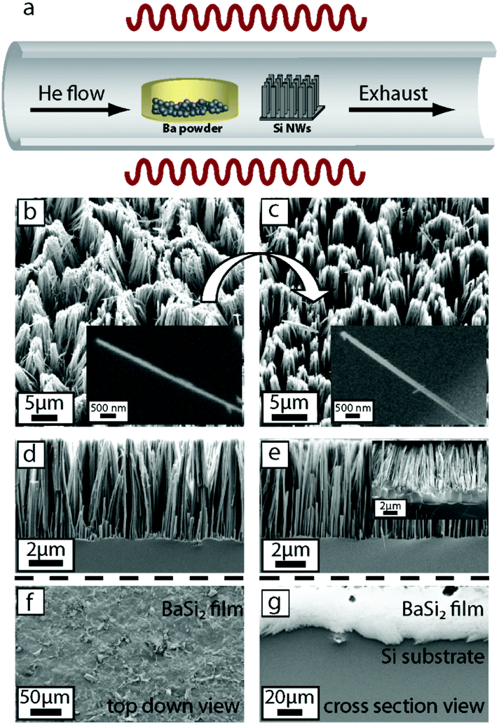 | ||
| Fig. 1 The conversion reaction set-up and the morphology of the starting and converted NWs and thin films. (a) A schematic showing the reaction setup; SEM micrographs (b–c) with a 30-degree tilt showing the morphology of (b) typical Si NW arrays before the conversion (inset shows an individual NW) and (c) the converted BaSi2 NW arrays (inset shows an individual NW); (d–g) cross section SEMs showing the morphology of (d) Si NW arrays and (e) BaSi2 NW arrays (inset shows the presence of BaSi2 film between the NW and Si substrate); (f) top-down view and (g) cross-section SEM images of the converted BaSi2 film on the Si chip. | ||
Structural characterization of BaSi2 NW arrays and thin films
As-converted NWs and thin films were mounted onto metallic pucks using double-sided carbon tape and imaged with a LEO Supra 55 VP field emission scanning electron microscope (SEM). Powder X-ray diffraction (PXRD) data were acquired on the as-converted arrays using a Bruker D8 ADVANCE powder diffractometer using Cu Kα radiation with a step size of 0.02 degrees. To perform energy dispersive spectroscopy (EDS) and transmission electron microscopy (TEM) on individual NWs, the converted NWs were scraped off the chip and dispersed in ethanol by sonication for ∼30 min at 100% power. The suspension was drop-casted onto TEM grids (Ted Pella, lacey carbon type-A on 300 mesh copper grids) and dried with N2. EDS characterization was completed using a LEO30 SEM with a SiLi X-ray detector. High-resolution TEM (HRTEM) was carried out using a FEI TITAN aberration-corrected scanning transmission electron microscope (STEM) operated at 200 kV.Optical and electrochemical measurements
Optical bandgap measurements of the as-converted NWs were taken in reflectance mode using a Jasco V-570 UV–vis near-infrared (NIR) spectrometer with an integrating sphere. A baseline was collected using the bare silicon substrate and subsequently subtracted from the collected reflectance data to remove any signal from the underlying Si substrate. In order to perform electrochemical measurements, electrodes were fabricated using the as-converted NWs on silicon substrate by back-contacting copper wire with Ga-In eutectic (≥99.99%) to the underlying degenerately-doped Si substrate and then coating with silver paint (Ted Pella). The electrodes were then electrically isolated with an insulating epoxy and cured overnight. J–V measurements were taken in a two-electrode configuration using a platinum mesh counter electrode and an electrolyte consisting of 0.5 M KI and 0.05 M I2 in anhydrous ethylene glycol. Electrochemical impedance spectroscopy (EIS) and Mott-Schottky measurements were performed in a solution of 0.1 M tetrabutylammonium perchlorate (TBAP) in anhydrous acetonitrile (≥99.0%) in a three-electrode configuration using a platinum mesh counter electrode and a Ag/AgCl reference electrode over the frequency range of 1 Hz to 5 MHz. All electrochemical measurements were performed using a Bio-Logic SP-200 potentiostat.Results and discussion
Synthesis and characterization of BaSi2 nanowire arrays and thin films
Successful vapor phase conversion of the Si NW arrays was performed inside a home-built CVD setup described previously17,18 and shown in Fig. 1a. The major challenges in these conversion reactions include: (i) providing sufficient kinetics for the conversion while preserving the nanoscale morphology and (ii) controllably forming the BaSi2 phase among the various Ba silicide phases (Ba2Si, Ba5Si3, BaSi, Ba3Si4 and BaSi2). We used electrochemically etched dense and well-ordered Si NW arrays still attached to the Si substrate (Fig. 1b) with lengths of approximately 5 μm (Fig. 1d) and average diameters of 123 ± 34 nm (estimated from SEM images of 20 examined NWs) as the initial nanostructures. These NWs can be produced in reasonable yield. We have previously shown that using the Si substrate as a continuous source of Si in excess is crucial in the formation of the most silicon-rich metal silicide phase without other phase impurities.36 As for the choice of precursor, we chose Ba beads because Ba has a relatively high vapor pressure of approximately 3.69 Torr at 1000 °C, which greatly facilitates the conversion reaction. We purposefully limited the amount of precursor in the system because our previous work36 demonstrated that limiting the metal precursor in the reaction system also favors the formation of the silicon-rich silicide. Moreover, by simply using a Si chip instead of Si NWs as the initial nanostructure, we can controllably form BaSi2 films on the silicon substrate. Therefore, by carefully controlling the reaction conditions in the optimized reactions described herein, we show that single-crystalline BaSi2 NW arrays and thin films can be successfully obtained by converting Si NW arrays and Si chips, respectively.The morphology of the as-converted NW arrays and films were examined using SEM (Fig. 1c, e, f and g). The converted NWs (Fig. 1c) appeared very similar to the initial nanostructures with lengths of approximately 5 μm (Fig. 1e) and an average diameter of 130 ± 52 nm (estimated from SEM images of 20 examined NWs). Some bundling of the nanostructures was observed in the final product, but for the most part, the converted nanostructures appeared vertical and separated. The converted films are approximately 10 μm thick (Fig. 1g) and created a uniform layer covering the entire silicon substrate. Successful vapor phase conversion also requires the formation of the BaSi2 phase without other major phase impurities. The PXRD patterns of the as-converted NW substrate and thin film (Fig. 2a) clearly show that most diffraction peaks can be successfully indexed to the BaSi2 phase (PDF #71-2327) with very minor Ba3Si4 and SiO2 impurity phases. We also analyzed the elemental composition of individual NWs using EDS by scanning individual NWs for their elemental composition. A total of five NWs were analyzed, and for each NW, a spectrum scan was performed on multiple locations along the length of the NW. A typical EDS spectrum (Fig. 2b) on one of the analyzed NWs (shown in Fig. 2b inset) revealed the presence of Ba, Si, Al, Cu, O, and C. The C, Al, and Cu signals arise from the TEM grid and sample holder and were subtracted for the compositional calculations. The calculations showed that the elemental Ba![[thin space (1/6-em)]](https://www.rsc.org/images/entities/char_2009.gif) :Si ratio in the converted nanostructures was approximately 1:2, very close to that of the BaSi2 phase.
:Si ratio in the converted nanostructures was approximately 1:2, very close to that of the BaSi2 phase.
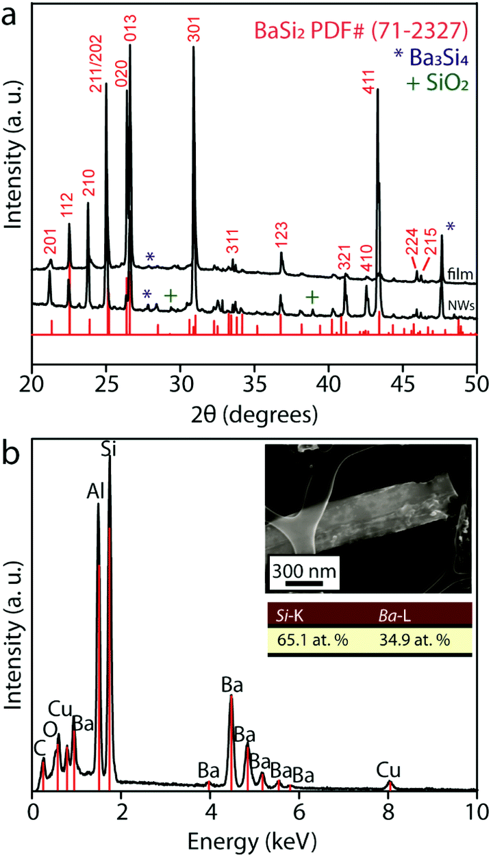 | ||
| Fig. 2 PXRD and EDS of the as-converted NWs and thin films. (a) PXRD of the as-converted film and NWs in comparison with the reference pattern for BaSi2 (PDF# 71-2327), with minor Ba3Si4 and SiO2 indicated by * and +, respectively; (b) EDS spectrum of a typical NW with quantification of the atomic percentage (shown in the inset) demonstrating the presence of Ba and Si and confirming the ratio of Ba:Si = 1:2 within the error of the EDS analysis. | ||
High-resolution transmission electron microscopy
The crystal structure of the converted NWs was further studied using TEM. We performed a thorough analysis of three NWs synthesized under the optimal conditions along their entire lengths and found that two of them were entirely single crystalline, and one NW demonstrated partial conversion, forming a Si/BaSi2 heterostructure (Fig. S1†). The completely converted NWs were analyzed at multiple locations along the length of the wire, and the crystallinity was verified by obtaining HRTEM micrographs on several spots. A low-magnification TEM image (Fig. 3a) shows a representative BaSi2 NW synthesized under the optimal conditions with a diameter of approximately 200 nm, and the inset electron diffraction pattern taken from the entire NW demonstrated only the [331] zone axis, therefore confirming the converted NW to be single crystalline. The HRTEM image (Fig. 3b) shows lattice fringes along the [331] zone axis, confirming the single-crystalline nature of the NW. The two-dimensional fast Fourier transform (FFT) of the lattice-resolved image (Fig. 3c) shows the reciprocal lattice peaks, which can be indexed to the orthorhombic BaSi2 lattice (space group Pnma, with a lattice constant of a = 8.92 Å, b = 6.75 Å and c = 11.57 Å).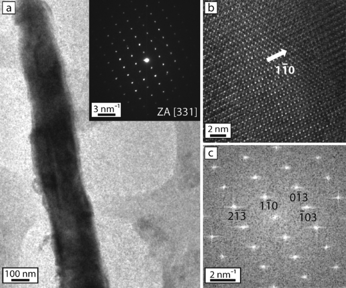 | ||
| Fig. 3 TEM micrographs of a representative BaSi2 NW synthesized under the optimal conditions. (a) Low-resolution TEM micrograph of a typical NW with inset showing the electron diffraction pattern taken over the entire NW, which confirms the single-crystalline nature of the NW; (b) lattice-resolved HRTEM micrograph along the [331] zone axis and (c) the corresponding indexed FFT pattern. | ||
Nanostructure control and temperature-independent synthesis of BaSi2 NW arrays
As mentioned previously, one of the major challenges in conversion reactions is to successfully perform the conversion while preserving the morphology of the initial nanostructures. It is therefore desirable to carry out the conversion at the lowest possible temperature to prevent severe loss of nanoscale morphology. However, in our previous HMS conversion work,36 we have seen that higher temperature favors the formation of the silicon-rich silicide and lowers the reaction temperature-introduced phase impurities in the products. Therefore, finding the optimal reaction conditions to synthesize the BaSi2 NWs described herein required a balance between these requirements. We performed the conversion reaction by placing the initial Si nanostructures at different distances from the center of the furnace and thus different reaction temperatures. We performed separate conversion reactions by placing the Si NWs at 2.2, 3.5 and 4.5 cm downstream from the center of the tube furnace where the alumina boat containing Ba was located (approximate temperatures of 980, 965 and 930 °C, respectively) and analyzed the morphology and phase of the final products after 2 h. The chip placed 2.2 cm downstream (closest to the center of the furnace) showed two distinct regions. The region closer to the center of the furnace looked like a dense film (Fig. 4a), and the region farther away looked like thicker bundles of NWs (Fig. 4b), which clearly showed severe loss of morphology from the initial nanostructures. PXRD patterns of these two regions, however, did not reveal any significant differences and indicated that both structures were entirely BaSi2 phase without any phase impurities (Fig. 4e and f). The products formed at 3.5 cm and 4.5 cm from the center of the furnace retained the initial NW morphology well, as compared to the products at 2.2 cm. In these products, however, some phase impurities in the form of Ba3Si4 and SiO2 were detectable by PXRD, as shown in Fig. 4g and h. However, these impurities are very minor compared to the major BaSi2 phase. Additionally, as the temperature decreased, we observed a decrease in the extent of bundling of the NWs, which resulted in a denser array of thinner individual NWs. Based on the morphology of the final product that was at about 930 °C, we take the reaction performed with the chip placed at 4.5 cm downstream from the furnace as the optimized conversion reaction to synthesize BaSi2 NWs.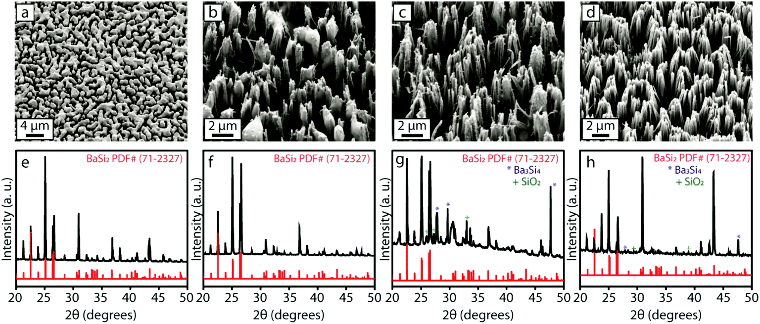 | ||
| Fig. 4 Role of the substrate position and reaction temperature on the morphology and phase of the converted nanostructures. SEM images of the final products formed at (a–b) 2.2 cm, (c) 3.5 cm, and (d) 4.5 cm downstream from the center of the furnace (which was set to 1000 °C) and their respective PXRD patterns (e–h), in comparison with the reference diffractogram for BaSi2 (PDF# 71-2327). The minor Ba3Si4 and SiO2 impurities are marked by * and +, respectively. | ||
It is interesting to note that the substrates placed closer to the center of the furnace showed significant loss of nanoscale morphology as compared to those placed further away from the center. We speculate that the Si NWs placed at higher temperatures (closer to the center) could have a very rapid flux of Ba depositing onto the substrate, which results in the formation of film-like structure. At lower temperatures (further away from the center of the furnace), Ba does not deposit as rapidly but can easily diffuse into the Si NWs, and the nanomorphology is still retained in these structures. It is also worth noting that significant phase impurities arise in the products placed farther away from the center of the furnace (even lower temperatures). This is similar to the HMS conversion work, where several phase impurities were observed at lower reaction temperatures.36 Furthermore, performing the BaSi2 conversion reaction for shorter amounts of time at higher temperatures (such as 1000 °C) also gave rise to several impurity phases in the final products (Fig. S2†). These observations suggest that the formation of BaSi2 could be a phase transformation process where several silicide phases are initially nucleated. However, at longer reaction times and higher temperatures, due to the higher mobility of Si, the most silicon-rich silicide, i.e. BaSi2, forms as the eventual product in this system.
Optical bandgap and electrochemical measurements
We observed two absorption onsets of ∼1 eV and ∼1.2 eV in the absorbance spectrum of BaSi2 NWs (Fig. 5a). Fitting the absorbance spectrum to Tauc plots corresponding to direct and indirect bandgap transitions and further extrapolating the linear regions of the fittings, we were able to determine a direct bandgap of 1.06 eV and an indirect bandgap of 1.27 eV for the BaSi2 NW arrays (Fig. 5b). These observed bandgaps are very close to previously calculated and reported values for BaSi2 thin films1,3,42,43 (although there are slight variations on the reported values in the literature). The difference in the morphology (NW vs. thin film) and the fabrication methods could cause slight variations between the reported bandgap values. To further study the electrical properties of the NW arrays, we performed electrochemical measurements of the BaSi2 NW arrays in the non-aqueous electrolyte ethylene glycol with a KI (0.5 M)/I2 (0.05 M) redox couple; the corresponding J–V curves (Fig. S3†) did not show any measureable photovoltage, although the NWs do show a photocurrent response (Fig. 5c), where 1 sun illumination resulted in an increased current of approximately 0.3 mA cm−2 at an applied voltage of 0.3 V. This observation is very similar to previous reports by several groups of a measurable photocurrent for BaSi2 film4,5,44 in solid-state junction devices. It is also worth mentioning that some previous photocurrent measurements of BaSi2 film on Si substrate reported that even when photo-excited carriers are generated in the BaSi2 layer, the recombination at the BaSi2/Si interface reduces the overall measured photocurrent.4,44,45 Therefore, it could also be possible that there was some electrical loss at the interface between the BaSi2 NWs and the underlying Si substrate. Further studies with careful control and tuning of the BaSi2/Si interface should be performed to systematically study these interfacial effects on the measurements. To further understand the observed conductivity and to determine the major carrier type of the NW arrays, we performed a Mott-Schottky analysis on the BaSi2 nanostructures in a solution of 0.1 M TBAP in anhydrous acetonitrile in a three-electrode configuration over the frequency range of 1 Hz to 5 MHz. The resulting Mott-Schottky plot (Fig. 5d) was then generated automatically as the inverse square of the space charge capacitance (1/CS2) as a function of the applied potential (V) using the accompanying Bio-Logic EC-Lab V10.40 software following the classical Mott-Schottky equation:
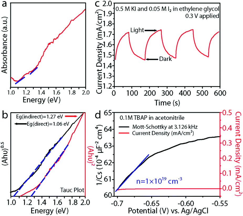 | ||
| Fig. 5 Optical and electrochemical properties of the BaSi2 NW arrays. (a) Absorbance spectrum of the BaSi2 NW arrays and (b) the corresponding Tauc plots confirming a direct bandgap transition of 1.06 eV and an indirect bandgap transition of 1.27 eV. (c) Photoresponse of BaSi2 NW arrays under intermittent 1 sun (100 mW cm−2) illumination with 0.3 V applied voltage showing a photocurrent of ∼0.3 mA cm−2. (d) Mott-Schottky analysis of the same NW array showing an n-type carrier concentration of 1 × 1019 cm−3. | ||
The constants of the Mott-Schottky equation are as follows: electron charge (e), the dielectric constant (ε), permittivity of free space (ε0), and flat-band potential (EFB). Fitting the slope of the Mott-Schottky plot revealed the BaSi2 NWs to be n-type with a carrier concentration of 1 × 1019 cm−3. The observed majority carrier type in our NW array is in agreement with previous reports on BaSi2 films; however, the reported carrier concentration is approximately 2–3 orders of magnitude larger as compared to previous reports.1,4,45 We speculate that the difference in carrier concentration could be caused by differences in our sample resulting from the different synthesis methods that yield high surface area nanostructures and the specific precursors that could introduce potential dopants or defects.
Conclusion
We have used the vapor phase conversion approach to selectively synthesize BaSi2 NW arrays for the first time by reacting arrays of Si NWs in a CVD tube furnace at 930 °C. We have conclusively characterized the structures, preliminarily examined their optical and electrochemical properties, and provided insights to the conversion mechanism. The NW morphology of the final products can be maintained with optimized reaction conditions, and by changing reaction parameters, BaSi2 thin films can also be formed. Optical bandgap measurements show that the NWs have direct and indirect bandgap of 1.06 and 1.27 eV, respectively, and preliminary electrochemical measurements suggest that the converted NWs are n-type with a carrier concentration of 1 × 1019 cm−3. These properties are very similar to values previously reported for BaSi2 thin film samples. These novel semiconducting BaSi2 NWs could be potentially explored for solar energy applications.Acknowledgements
This work was supported by a Research Corporation Scialog Collaborative Award for Solar Energy Conversion. L. S. also thanks the support from the NSF Graduate Research Fellowship Program.References
- K. Morita, Y. Inomata and T. Suemasu, Thin Solid Films, 2006, 508, 363–366 CrossRef CAS PubMed.
- K. Morita, M. Kobayashi and T. Suemasu, Thin Solid Films, 2007, 515, 8216–8218 CrossRef CAS PubMed.
- T. Suemasu, Jpn. J. Appl. Phys., 2015, 54, 07JA01 CrossRef.
- W. Du, M. Baba, K. Toko, K. O. Hara, K. Watanabe, T. Sekiguchi, N. Usami and T. Suemasu, J. Appl. Phys., 2014, 115, 223701 CrossRef PubMed.
- W. Du, R. Takabe, M. Baba, H. Takeuchi, K. O. Hara, K. Toko, N. Usami and T. Suemasu, Appl. Phys. Lett., 2015, 106, 122104 CrossRef PubMed.
- M. J. Bierman and S. Jin, Energy Environ. Sci., 2009, 2, 1050–1059 CAS.
- A. I. Hochbaum and P. Yang, Chem. Rev., 2010, 110, 527–546 CrossRef CAS PubMed.
- T. J. Kempa, R. W. Day, S.-K. Kim, H.-G. Park and C. M. Lieber, Energy Environ. Sci., 2013, 6, 719–733 CAS.
- M. Cabán-Acevedo, D. Liang, K. S. Chew, J. P. DeGrave, N. S. Kaiser and S. Jin, ACS Nano, 2013, 7, 1731–1739 CrossRef PubMed.
- M. Pani and A. Palenzona, J. Alloys Compd., 2008, 454, L1–L2 CrossRef CAS PubMed.
- A. L. Schmitt, J. M. Higgins, J. R. Szczech and S. Jin, J. Mater. Chem., 2010, 20, 223–235 RSC.
- A. L. Schmitt, M. J. Bierman, D. Schmeisser, F. J. Himpsel and S. Jin, Nano Lett., 2006, 6, 1617–1621 CrossRef CAS PubMed.
- A. L. Schmitt, L. Zhu, D. Schmeisser, F. J. Himpsel and S. Jin, J. Phys. Chem. B, 2006, 110, 18142–18146 CrossRef CAS PubMed.
- Y.-H. Liang, S.-Y. Yu, C.-L. Hsin, C.-W. Huang and W.-W. Wu, J. Appl. Phys., 2011, 110, 074302 CrossRef PubMed.
- A. L. Schmitt, J. M. Higgins and S. Jin, Nano Lett., 2008, 8, 810–815 CrossRef CAS PubMed.
- J. M. Higgins, P. Carmichael, A. L. Schmitt, S. Lee, J. P. Degrave and S. Jin, ACS Nano, 2011, 5, 3268–3277 CrossRef CAS PubMed.
- J. M. Higgins, R. Ding, J. P. DeGrave and S. Jin, Nano Lett., 2010, 10, 1605–1610 CrossRef CAS PubMed.
- J. M. Higgins, R. Ding and S. Jin, Chem. Mater., 2011, 23, 3848–3853 CrossRef CAS.
- J. M. Higgins, A. L. Schmitt, I. A. Guzei and S. Jin, J. Am. Chem. Soc., 2008, 130, 16086–16094 CrossRef CAS PubMed.
- J. R. Szczech, A. L. Schmitt, M. J. Bierman and S. Jin, Chem. Mater., 2007, 19, 3238–3243 CrossRef CAS.
- Y. Song, A. L. Schmitt and S. Jin, Nano Lett., 2007, 7, 965–969 CrossRef CAS PubMed.
- Y. Song and S. Jin, Appl. Phys. Lett., 2007, 90, 173122 CrossRef PubMed.
- Y. Wu, J. Xiang, C. Yang, W. Lu and C. M. Lieber, Nature, 2004, 430, 61–65 CrossRef CAS PubMed.
- Y. Chen, Y.-C. Lin, C.-W. Huang, C.-W. Wang, L.-J. Chen, W.-W. Wu and Y. Huang, Nano Lett., 2012, 12, 3115–3120 CrossRef CAS PubMed.
- Y. Chen, Y.-C. Lin, X. Zhong, H.-C. Cheng, X. Duan and Y. Huang, Nano Lett., 2013, 13, 3703–3708 CrossRef CAS PubMed.
- W.-L. Chiu, C.-H. Chiu, J.-Y. Chen, C.-W. Huang, Y.-T. Huang, K.-C. Lu, C.-L. Hsin, P.-H. Yeh and W.-W. Wu, Nanoscale Res. Lett., 2013, 8, 290 CrossRef PubMed.
- K.-C. Lu, W.-W. Wu, H.-W. Wu, C. M. Tanner, J. P. Chang, L. J. Chen and K. N. Tu, Nano Lett., 2007, 7, 2389–2394 CrossRef CAS PubMed.
- K. Yamamoto, H. Kohno, S. Takeda and S. Ichikawa, Appl. Phys. Lett., 2006, 89, 083107 CrossRef PubMed.
- Y.-C. Lin, K.-C. Lu, W.-W. Wu, J. Bai, L. J. Chen, K. N. Tu and Y. Huang, Nano Lett., 2008, 8, 913–918 CrossRef CAS PubMed.
- B. Liu, Y. Wang, S. Dilts, T. S. Mayer and S. E. Mohney, Nano Lett., 2007, 7, 818–824 CrossRef CAS PubMed.
- K.-C. Lu, W.-W. Wu, H. Ouyang, Y.-C. Lin, Y. Huang, C.-W. Wang, Z.-W. Wu, C.-W. Huang, L. J. Chen and K. N. Tu, Nano Lett., 2011, 11, 2753–2758 CrossRef CAS PubMed.
- H.-B.-R. Lee, G. H. Gu, C. G. Park and H. Kim, J. Electrochem. Soc., 2012, 159, K146–K151 CrossRef CAS PubMed.
- Y.-C. Lin, Y. Chen, R. Chen, K. Ghosh, Q. Xiong and Y. Huang, Nano Lett., 2012, 12, 4341–4348 CrossRef CAS PubMed.
- Y.-C. Lin, Y. Chen, A. Shailos and Y. Huang, Nano Lett., 2010, 10, 2281–2287 CrossRef CAS PubMed.
- Y.-H. Hsieh, C.-H. Chiu, C.-W. Huang, J.-Y. Chen, W.-J. Lin and W.-W. Wu, Nanoscale, 2015, 7, 1776–1781 RSC.
- A. Pokhrel, Z. P. Degregorio, J. M. Higgins, S. N. Girard and S. Jin, Chem. Mater., 2013, 25, 632–638 CrossRef CAS.
- L.-W. Chu, C.-W. Hung, C. Y. Wang, Y.-H. Chen, J. Tang, K. L. Wang and L.-J. Chen, J. Electrochem. Soc., 2011, 15, K64–K68 CrossRef PubMed.
- H. Liu, G. She, X. Huang, X. Qi, L. Mu, X. Meng and W. Shi, J. Phys. Chem. C, 2013, 117, 2377–2381 CAS.
- Y. Kang and S. Vaddiraju, Chem. Mater., 2014, 26, 2814–2819 CrossRef CAS.
- S. Lee, J. Yoon, B. Koo, D. H. Shin, J. H. Koo, C. J. Lee, Y.-W. Kim, H. Kim and T. Lee, IEEE Trans. Nanotechnol., 2013, 12, 704–711 CrossRef CAS.
- K. Peng, Y. Yan, S. Gao and J. Zhu, Adv. Funct. Mater., 2003, 13, 127–132 CrossRef CAS PubMed.
- T. Nakamura, T. Suemasu, K.-i. Takakura, F. Hasegawa, A. Wakahara and M. Imai, Appl. Phys. Lett., 2002, 81, 1032–1034 CrossRef CAS PubMed.
- Y. Matsumoto, D. Tsukada, R. Sasaki, M. Takeishi and T. Suemasu, Appl. Phys. Express, 2009, 2, 021101 CrossRef.
- T. Suemasu, T. Saito, K. Toh, A. Okada and M. A. Khan, Thin Solid Films, 2011, 519, 8501–8504 CrossRef CAS PubMed.
- K. O. Hara, N. Usami, K. Toh, M. Baba, K. Toko and T. Suemasu, J. Appl. Phys., 2012, 112, 083108 CrossRef PubMed.
Footnote |
| † Electronic supplementary information (ESI) available. See DOI: 10.1039/c5nr03668b |
| This journal is © The Royal Society of Chemistry 2015 |