
 Open Access Article
 This Open Access Article is licensed under a Creative Commons Attribution-Non Commercial 3.0 Unported Licence
A mesoporous nickel counter electrode for printable and reusable perovskite solar cells
Zhiliang
Ku
a,
Xinhui
Xia
a,
He
Shen
a,
Nguyen Huy
Tiep
ab and
Hong Jin
Fan
*a
aSchool of Physical and Mathematical Sciences, Nanyang Technological University, 637371, Singapore. E-mail: fanhj@ntu.edu.sg
bInterdisciplinary Graduate School, Nanyang Technological University, 639798, Singapore
First published on 6th July 2015
Abstract
A mesoporous nickel layer is used as the counter electrode in printable perovskite solar cells. A unique reuse process is realized in such perovskite solar cell devices by repeated loading of the perovskite material. Under standard AM1.5 illumination, the fresh device shows a promising power conversion efficiency of 13.6%, and an efficiency of 12.1% is obtained in the reused devices.
In the past few decades, solid state junction solar cells with high efficiency and excellent stability, usually made of silicon and compound semiconductors, have dominated the commercial market of photovoltaics. But these photovoltaic technologies still have constraints in further market development due to both expensive materials and tedious manufacturing processes.1 Since the end of the last century, emerging photovoltaic technologies such as organic cells,2,3 inorganic cells,4 quantum dot cells5,6 and dye-sensitized solar cells,7 have drawn increasing interests because of the cost-effective solution-processed materials. In these solution-processed photovoltaics, light-absorber and electrode materials can be applied to the substrate by techniques such as blade coating, spray coating, printing and slot-die coating. It is apparent that these low-temperature techniques can significantly reduce the energy cost associated with solar-cell manufacturing and therefore the energy payback time. However for a long time, the solar power conversion efficiency (PCE) of these solar cells has not exceeded 15%, let alone that of silicon solar cells. Fortunately, in recent years, the emergence of organic–inorganic hybrid perovskite materials has injected new hope into the development of such solution-processed high PCE photovoltaics.
Since methylammonium lead iodide (CH3NH3PbI3) made its debut as a light-harvesting material for DSSCs in 2009,8 organic–inorganic halide perovskites (CH3NH3PbX3, X = Cl, Br, I) have demonstrated huge potential as a light absorber due to their large photon absorption coefficients over the entire visible range and their long-range balanced charge carrier diffusion lengths.9–14 In a short time, enormous attention has been focused on perovskite solar cells (PSCs) and a series of strategies have been successfully developed to improve the PCE, including the device structure, interfacial engineering, chemical compositional tuning, and the crystallization kinetics control.11,15–25 As a result, in a short time, the PCE of PSCs has skyrocketed to over 19%,25 which is comparable to that of the commercial silicon solar cells. Such high efficiency together with the cost-effective materials and processes for PSCs make them economically viable for commercialization (provided that the stability issue has been addressed).
Most of the high-efficiency PSCs, however, still need a noble metal such as Au or Ag as the counter electrode (CE). They are typically prepared by vacuum thermal or e-beam evaporation. Elimination of the vacuum facility is always desirable from the cost point of view. Recently, the Han group pioneered the use of carbon CE in PSCs and obtained a certified PCE up to 12.8%.17,26 In comparison with the noble metal, this carbon CE, which can be printed on PSCs, shows a more promising prospect for fabricating low-cost, large-scale solar cells. But the problem of carbon materials is their fragility, especially when their thickness is increased in order to have low sheet resistance. Thus, replacing the carbon (as well as Au and Ag) CEs by cheap and robust ones will be technically important for the printable PSCs.
Recently, Xu and co-workers reported that nickel can perform as an effective CE in PSCs.27 They fabricated the PSC by sputtering nickel instead of Au on hole-transporting materials. Such nickel-cathode PSCs showed a promising PCE of 10.4%, which was very close to the Au version (11.6%). Based on their pioneering work, in this work, we employed a mesoporous nickel (mpNi) film as a printable CE for PSC. Meanwhile, for the first time, we demonstrate that this mpNi-cathode PSC device can be reused by washing and reloading the perovskite material. As is well known, the organic–inorganic halide perovskite is very sensitive to moisture and oxygen, and this instability has become a major obstacle to its outdoor applications. However, in our case, the degraded perovskite can be washed off from the device and fresh perovskite can be reloaded. We believe that this unique reuse technology can extend the service time of PSC devices, and may open a new door to the further development of low-cost PSCs. Under standard AM1.5 illumination, our fresh mpNi-cathode PSCs show an outstanding PCE of 13.6%; and the reused one still has an acceptable PCE of 12.1%, which is 89% of its initial value.
Fig. 1a shows the structure of the printable PSC device made of an ALD TiO2 block layer (30 nm thick), a TiO2 nanocrystalline layer (500 nm thick), an Al2O3 paste (∼1 μm thick) and mp-NiO films (∼2 μm thick). Details of the preparation method are described in the Experimental details section. During annealing in the presence of hydrogen at 350 °C, the as-pasted NiO film on the top of the device will be reduced into Ni based on the following reaction:28
| NiO + H2 → Ni + H2O(1) | (1) |
 | ||
| Fig. 1 (a) The schematics of the printable perovskite solar cell device containing a mesoporous nickel (mpNi) counter electrode. (b) The corresponding energy levels. | ||
This reducing process is irreversible and leads to the formation of the mpNi-cathode device.
Fig. 1b shows the diagram of relative energy levels of this mpNi-cathode PSC. This configuration allows the photo-generated electron–hole pairs within the perovskite (CH3NH3PbI3) to be separated; electrons on the conduction band (−3.9 eV) and the holes on the valence band (−5.4 eV) will transfer to TiO2 (conduction band at −4.0 eV) and to nickel CE (conductive band −5.0 eV), respectively, forming a photocurrent in the circuit.
A two-step sequential method was employed to load the perovskite into mpNi-cathode PSCs.29 To do this, the as-made mesoporous device was dipped sequentially into a PbI2 precursor and methylammonium iodide (CH3NH3I) solution (see the Experimental details section). After drying at 70 °C for 30 min, the resulting device showed a black color, as seen from the photoanode side, demonstrating the formation of a perovskite and completion of the fabrication of devices. The composition change in the PSC device was characterized by X-ray diffraction (XRD) measurements. As seen in Fig. 2, the XRD spectrum of FTO/TiO2/Al2O3/NiO films showed the peaks at 37.28°, 43.25° and 62.72°, corresponding to the (111), (200) and (220) lattice planes of NiO. After the annealing in hydrogen-containing ambience, the peaks of NiO vanished and a strong peak showed up at 44.51°, indicating the complete transformation of NiO to Ni. After filling PbI2 into the device, we can observe two new peaks at 12.67° and 39.52°, which belong to the (001) and (110) lattice planes of PbI2. In the final device, a series of new diffraction peaks appear that are in good agreement with the tetragonal phase of the CH3NH3PbI3 perovskite.30 Obviously, the conversion of PbI2 is complete, as is evident from the disappearance of its most intense (001) peak.
 | ||
| Fig. 2 XRD patterns of the PSC device with different components. | ||
The electric conductivity of the mpNi films was measured using four-probe tests and compared with that of carbon films31 of the same thicknesses. The square resistance (Rsq) values of the nickel and carbon films in sizes of 2 cm × 2 cm are shown in Table 1. We can see that the mpNi films have Rsq one order of magnitude lower than the carbon film in all three thicknesses. At 2 μm thickness, obviously the carbon film is not suitable for CE for PSC because of its poor conductivity. In contrast, the mpNi film with the same thickness of 2 μm has an acceptable Rsq of 38.22 Ω □−1. For our printable PSC device, a thinner CE electrode will be propitious to the permeation of the CH3NH3PbI3 precursor deep into the Al2O3 layer. Hence, in our study we employed the ∼2 μm thick mesoporous nickel films as CEs for the devices.
| Film | 2 μm | 6 μm | 10 μm |
|---|---|---|---|
| Carbon | 575.21 Ω □−1 | 58.36 Ω □−1 | 10.47 Ω □−1 |
| Nickel | 38.22 Ω □−1 | 5.52 Ω □−1 | 1.96 Ω □−1 |
Fig. 3a shows the microstructure of the mpNi-cathode PSC device. We can clearly see that the nickel film possesses a mesoporous structure, which consists of nickel nanoparticles with an average size of about 100 nm. The insulating Al2O3 film was used as a spacer layer to separate the nickel and TiO2 layers, ensuring that there was no risk of direct contact between the CE and photoanode. Based on our previous study,17,26,29 the thickness of the Al2O3 spacer layer and TiO2 active layer were controlled to about 1 μm and 500 nm, respectively. Since all the films in this device are relatively thin and porous, CH3NH3PbI3 can easily be loaded into the device by the facile two-step sequential method. Fig. 3b shows the filling of CH3NH3PbI3 in the device. In comparison with the bare TiO2 (Fig. 3c), most of the vacancies in the TiO2 layer were occupied homogeneously after the loading of CH3NH3PbI3, which is favorable for enhancing the PCE of the device.
 | ||
| Fig. 3 SEM images of the cross section of the PSC devices. (a) Artificially-colored mpNi-cathode PSC. (b) CH3NH3PbI3 coated TiO2 film. (c) Bare TiO2 film. | ||
It should be noted that, in this mpNi-cathode PSC device, the CE was fabricated before the loading of perovskite. This is unique because it means that the perovskite can be reloaded into the device many times. Here, we attempt to simulate the degradation of perovskite by exposing it in humid air and then washing it off, followed by reloading fresh perovskite into the device. As shown in Fig. 4, one mpNi-cathode PSC device (marked as A) was firstly filled with PbI2 by the drop-coating method, rendering a yellow color of the device seen from the photoanode side. Then, by reacting with CH3NH3I, device A changed its color from yellow to black, indicating the formation of CH3NH3PbI3. After exposing the as-obtained device without encapsulation in humid air for several days, the perovskite in device A will partially degrade because of reaction with H2O and O2.32 Generally, once this degradation process occurs, the PCE of the device will decrease sharply and irreversibly, especially in those planar PSC devices with metal cathodes. However, there is a quite different situation in our device. We used N,N-dimethylformamide (DMF) to wash away the degraded perovskite in device A. After that, we repeated the loading process of perovskite for the second time, obtaining the reused PSC device (device A+).
 | ||
| Fig. 4 The reuse process of the mpNi-cathode PSC device. | ||
Under AM1.5 simulated sunlight of 100 mW cm−2, the mpNi-cathode PSC device (device A) exhibits an open-circuit voltage (Voc) of 953 mV, a short-circuit current density (Jsc) of 19.1 mA cm−2 and a fill factor (FF) of 0.75, yielding a PCE of 13.6% (see Fig. 5 and Table 2). After being exposed in humid air for several days, the PCE of the device (called “degraded device A”) dropped to 6.59%, as a result of the degradation of CH3NH3PbI3. Finally, we “renewed” the degraded device by reloading fresh CH3NH3PbI3 into the same device. Such obtained device A+ can still produce a decent PCE of 12.1% (Jsc = 18.0 mA cm−2, Voc = 937 mV, FF = 0.72), which is much higher than the degraded vision.
 | ||
| Fig. 5 J–V curves of the mpNi-cathode PSC device in this study under AM1.5 simulated sunlight. | ||
| Device | J sc (mA cm−2) | V oc (mV) | FF | PCE (%) |
|---|---|---|---|---|
| A | 19.1 | 953 | 0.75 | 13.6 |
| A+ | 18.0 | 937 | 0.72 | 12.1 |
| Degraded A | 14.5 | 874 | 0.52 | 6.59 |
The incident photon-to-current conversion efficiency (IPCE) signifies the light response of the solar device and is directly related to the Jsc. The IPCE spectra of the above mentioned three types of mpNi-cathode PSC devices are presented in Fig. 6. Both device A and A+ show excellent photoresponse from 350 to 800 nm, with IPCE reaching 83% and 80% at the wavelengths between 400 and 600 nm, respectively. The IPCE of the degraded device A has a much lower value than device A in the full spectrum region from 350 to 800 nm. Moreover, the degraded device A shows a slightly different IPCE curve profile from those of device A and device A+. We ascribe this difference in the curve shape to the composition changes in degraded CH3NH3PbI3. By calculating the IPCE data according to the standard AM1.5 solar spectra, the integrated Jsc of the devices are obtained: device A: 18.9 mA cm−2, device A+: 17.9 mA cm−2, and degraded device A: 14.7 mA cm−2. These values are quite coincident with those measured in the J–V curves.
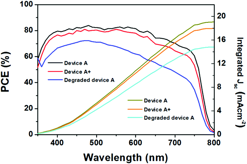 | ||
| Fig. 6 IPCE spectra and the integrated photocurrents of the mpNi-cathode PSC device. | ||
To investigate the reproducibility of the reuse process, we also measured the PCE changes in different devices. As shown in Fig. 7, ten mpNi-cathode PSC devices were measured under standard AM1.5 conditions immediately after the fabrication. These devices exhibited an average PCE of 13.02%. After being degraded in humid air, the average PCE of these devices dropped to 6.12%, which is only 47% of their initial average PCE. However, by washing and reloading the perovskite into the degraded devices, the average PCE of these reused devices was enhanced to 11.63%, reaching 89.3% of their initial average value. We note that it is challenging to fully recover the PCE because of some damage happened to the mpNi films during the washing process. Despite that, the reusable mesoporous metal-cathode PCSs provide a promising approach towards low-cost PSC with a long service life.
 | ||
| Fig. 7 Efficiency variation of ten different PSC devices under different conditions: fresh, reused, and degraded. | ||
In summary, we have demonstrated the successful employment of a mesoporous Ni thin film as a printable counter electrode for perovskite solar cells. The mpNi film with a thickness of 2 μm shows a favorable conductivity. By using this mpNi film, we fabricated the mpNi-cathode PSC devices and obtained a PCE of 13.6% under standard AM1.5 conditions. Moreover, for the first time, a reuse process is achieved in these mpNi-cathode PSC devices by washing and reloading perovskite. While the air-exposed PSC devices (no encapsulation) lose their PCE by more than 50%, our reuse process can recover almost 90% of their initial PCE. We are optimistic that this unique reuse process in our mesoporous metal-cathode PSC devices possesses a great potential for developing low-cost, fully-printable solar cells with high efficiency and long service life.
Experimental details
Preparation of Al2O3, NiO and carbon pastes
The fabrication processes for the Al2O3 and NiO pastes are similar. Specifically, 1 g hydroxypropyl cellulose was dissolved in 20 ml ethanol and 20 mL terpineol solution. Then, 1 g Al2O3 or NiO powder was added into the solution, followed by stirring vigorously using ball milling for 6 h. After removing the ethanol solvent by reduced pressure distillation, the paste was obtained. A carbon paste was prepared following the recipe reported previously.31Fabrication of the mpNi-cathoded PSC device
The fluorine-doped SnO2 substrates were etched with a compound containing zinc powder and hydrochloric acid (1 M) to form two detached electrode patterns before being ultrasonically cleaned with detergent, deionized water and ethanol successively. After that, the patterned substrates were coated with a 30 nm compact TiO2 layer by the atomic deposition method (ALD) at 120 °C. After cooling down to room temperature naturally, a 500 nm TiO2 nanocrystalline layer (PASOL HPW-18NR) was deposited on top of the compact layer by screen printing and then sintered at 500 °C for 30 min. After that, a 1 μm thick Al2O3 spacer layer and a 2 μm thick mesoporous NiO layer were printed on the top of the TiO2 nanocrystalline layer successively. After being dried on a hot plate, the films were sintered in a quartz tube at 500 °C for 30 min under an oxygen atmosphere, and then for another 30 min under a hydrogen atmosphere (2% in argon) at 350 °C. After that they cooled down naturally to room temperature.To complete the PSC device, the last step was to add the perovskite. Briefly, 2 μL of the PbI2 precursor (0.578 g PbI2 dissolved in 1 mL DMF) was dropped on the top of the mesoporous Ni layer. Then the devices were dried at 70 °C on a hot plate. After cooling down, the devices were dipped into a methylammonium iodide (CH3NH3I) isopropanol (IPA) solution (10 mg mL−1) for 10 min. After drying at 70 °C in an oven for 30 min, the resulting perovskite films appear black as seen from the photoanode side, demonstrating the completion of the fabrication of devices.
Reuse process of the mpNi-cathoded PSC device
The reuse process of the device was carried out by dipping the device into the DMF solvent for 30 min at room temperature. Then, the device was washed with ethanol three times and then dried on a hot plate at 100 °C for 10 min. Finally, the perovskite was reloaded into the device by the two-step process mentioned above.Characterization
Conductivity of the nickel and carbon films (both are 2 cm × 2 cm in sizes) was measured using the standard four-probe test. The composition and microstructure of the PSC devices were characterized by X-ray diffraction (XRD, Rigaku D/Max-2550 with Cu Kα radiation) and field emission scanning electron microscopy (FESEM, FEI Sirion). The photocurrent density–voltage (J–V) characteristics were recorded with a Keithley 2400 source meter under illumination with a solar simulator (Oriel) composed of a 1000 W xenon arc lamp and an AM1.5 G filter. The light intensity was calibrated using a standard silicon cell. A black mask with a circular aperture (0.159 cm2) smaller than the active area of the square solar cell (0.5 cm2) was applied on top of the cell. The normalized incident-photon-to-electron conversion efficiencies (IPCE) were measured using a 150 W xenon lamp (Oriel) fitted with a monochromator (Cornerstone 74004) as a monochromatic light source.Acknowledgements
This work was supported by the Singapore-Berkeley Research Initiative for Sustainable Energy (SinBeRISE) program and the Singapore Ministry of Education Academic Research Fund Tier 3 (MOE2011-T3-1-005).Notes and references
- M. Graetzel, R. A. J. Janssen, D. B. Mitzi and E. H. Sargent, Nature, 2012, 488, 304–312 CrossRef CAS PubMed.
- T. Ameri, P. Khoram, J. Min and C. J. Brabec, Adv. Mater., 2013, 25, 4245–4266 CrossRef CAS PubMed.
- D. Carsten and D. Vladimir, Rep. Prog. Phys., 2010, 73, 096401 CrossRef.
- T. Todorov and D. B. Mitzi, Eur. J. Inorg. Chem., 2010, 2010, 17–28 CrossRef PubMed.
- P. V. Kamat, J. Phys. Chem. Lett., 2013, 4, 908–918 CrossRef CAS.
- E. H. Sargent, Nat. Photonics, 2012, 6, 133–135 CrossRef CAS PubMed.
- B. O'Regan and M. Gratzel, Nature, 1991, 353, 737–740 CrossRef PubMed.
- A. Kojima, K. Teshima, Y. Shirai and T. Miyasaka, J. Am. Chem. Soc., 2009, 131, 6050–6051 CrossRef CAS PubMed.
- J. H. Im, C. R. Lee, J. W. Lee, S. W. Park and N. G. Park, Nanoscale, 2011, 3, 4088–4093 RSC.
- H. S. Kim, C. R. Lee, J. H. Im, K. B. Lee, T. Moehl, A. Marchioro, S. J. Moon, R. Humphry-Baker, J. H. Yum, J. E. Moser, M. Gratzel and N. G. Park, Sci. Rep., 2012, 2, 591 Search PubMed.
- M. M. Lee, J. Teuscher, T. Miyasaka, T. N. Murakami and H. J. Snaith, Science, 2012, 338, 643–647 CrossRef CAS PubMed.
- J. H. Heo, S. H. Im, J. H. Noh, T. N. Mandal, C.-S. Lim, J. A. Chang, Y. H. Lee, H.-j. Kim, A. Sarkar, K. NazeeruddinMd, M. Gratzel and S. I. Seok, Nat. Photonics, 2013, 7, 486–491 CrossRef CAS PubMed.
- S. D. Stranks, G. E. Eperon, G. Grancini, C. Menelaou, M. J. Alcocer, T. Leijtens, L. M. Herz, A. Petrozza and H. J. Snaith, Science, 2013, 342, 341–344 CrossRef CAS PubMed.
- G. Xing, N. Mathews, S. Sun, S. S. Lim, Y. M. Lam, M. Gratzel, S. Mhaisalkar and T. C. Sum, Science, 2013, 342, 344–347 CrossRef CAS PubMed.
- S. Kazim, M. K. Nazeeruddin, M. Graetzel and S. Ahmad, Angew. Chem., Int. Ed., 2014, 53, 2812–2824 CrossRef CAS PubMed.
- J. Y. Jeng, Y. F. Chiang, M. H. Lee, S. R. Peng, T. F. Guo, P. Chen and T. C. Wen, Adv. Mater., 2013, 25, 3727–3732 CrossRef CAS PubMed.
- Z. Ku, Y. Rong, M. Xu, T. Liu and H. Han, Sci. Rep., 2013, 3, 3132 Search PubMed.
- S. Colella, E. Mosconi, P. Fedeli, A. Listorti, F. Gazza, F. Orlandi, P. Ferro, T. Besagni, A. Rizzo, G. Calestani, G. Gigli, F. De Angelis and R. Mosca, Chem. Mater., 2013, 25, 4613–4618 CrossRef CAS.
- N. J. Jeon, J. H. Noh, Y. C. Kim, W. S. Yang, S. Ryu and S. I. Seok, Nat. Mater., 2014, 13(9), 897–903 CrossRef CAS PubMed.
- J. Burschka, N. Pellet, S. J. Moon, R. Humphry-Baker, P. Gao, M. K. Nazeeruddin and M. Gratzel, Nature, 2013, 499, 316–319 CrossRef CAS PubMed.
- N. J. Jeon, J. H. Noh, W. S. Yang, Y. C. Kim, S. Ryu, J. Seo and S. I. Seok, Nature, 2015, 517, 476–480 CrossRef CAS PubMed.
- M. Liu, M. B. Johnston and H. J. Snaith, Nature, 2013, 501, 395–398 CrossRef CAS PubMed.
- D. Liu and T. L. Kelly, Nat. Photonics, 2014, 8, 133–138 CrossRef CAS PubMed.
- W. Nie, H. Tsai, R. Asadpour, J.-C. Blancon, A. J. Neukirch, G. Gupta, J. J. Crochet, M. Chhowalla, S. Tretiak, M. A. Alam, H.-L. Wang and A. D. Mohite, Science, 2015, 347, 522–525 CrossRef CAS PubMed.
- H. Zhou, Q. Chen, G. Li, S. Luo, T.-B. Song, H.-S. Duan, Z. Hong, J. You, Y. Liu and Y. Yang, Science, 2014, 345, 542–546 CrossRef CAS PubMed.
- A. Mei, X. Li, L. Liu, Z. Ku, T. Liu, Y. Rong, M. Xu, M. Hu, J. Chen, Y. Yang, M. Gratzel and H. Han, Science, 2014, 345, 295–298 CrossRef CAS PubMed.
- Q. Jiang, X. Sheng, B. Shi, X. Feng and T. Xu, J. Phys. Chem. C, 2014, 118, 25878–25883 CAS.
- J. Richardson, Appl. Catal., A, 2003, 246, 137–150 CrossRef CAS.
- Y. Rong, Z. Ku, A. Mei, T. Liu, M. Xu, S. Ko, X. Li and H. Han, J. Phys. Chem. Lett., 2014, 5, 2160–2164 CrossRef CAS.
- T. Baikie, Y. Fang, J. M. Kadro, M. Schreyer, F. Wei, S. G. Mhaisalkar, M. Graetzel and T. J. White, J. Mater. Chem. A, 2013, 1, 5628 CAS.
- H. Han, L. Zhang, T. Liu, L. Liu, M. Hu, Y. Yang and A. Mei, J. Mater. Chem. A, 2014, 3(17), 9165–9170 Search PubMed.
- G. Niu, X. Guo and L. Wang, J. Mater. Chem. A, 2015, 3(17), 8970–8980 CAS.
| This journal is © The Royal Society of Chemistry 2015 |